Category Archives: 3D Integration

January 15, 2010 – Allvia says it has completed integration and full reliability testing of a silicon interposer between a semiconductor die and an organic or ceramic substrate.

The company says it has solved the problem involved with 3D stacking of various compositions of substrate materials with different coefficients of thermal expansion, by putting the Si interposer between two stacked substrates and connecting them with through-silicon vias (TSV).

Using Si interposers also eliminates the need to requalify die with feature-size shrinks and changing pitch; and it avoids costs incurred from having to use more expensive substrates. (The company’s TSV work with flip-chips on the backside enables it to make cost-effective silicon interposers, added Sergey Savastiouk, CEO of Allvia, in a statement.) There are no material mismatches in such "hybrid substrates" with silicon on top and organic substrate beneath, as long as device reliability is confirmed, the company noted.

"There is a big difference between what we are demonstrating and multi-chip modules because we can build passive elements right onto the silicon substrate," noted Savastiouk.

January 8, 2009 – Living up to its pledge of an "integrated fabless manufacturing" (IFM) model, fabless giant Qualcomm has made two deals to reserve leading-edge semiconductor manufacturing capacity: one with longtime partner TSMC, and the other with foundry upstart GlobalFoundries.

The longtime customer of TSMC (they worked closely at 65nm in 2006 and ported to 45nm in 2007) now will jump ahead to 28nm for the fabless company’s system-on-chip technology, where density is twice that of previous nodes; work will involve both high-power high-k/metal gate (HKMG) and silicon oxynitride (SiON) low power versions, with tapeouts expected by mid-2010.

Meanwhile, Qualcomm says it is saddling up with GlobalFoundries for both 45nm and 28nm low-power processes, plus "an intended collaboration on future advanced process nodes." The first part of the arrangement will target the firm’s wireless business, providing technologies for handhelds and smartbook devices using various cellular standards (CDMA2000, WCDMA, 4G/LTE); designs will be sent later this year to GlobalFoundries’ Fab 1 in Dresden, Germany. The two also plan do explore other areas such as die-package interaction and 3D packaging technologies, but did not offer specific areas of focus or timelines.

Editor’s Take

On the one hand, Qualcomm is simply being smart in spreading its manufacturing around and mitigating risk. The work with TSMC seems targeted for systems-on-chip DSP for cell phones, continuing work on products the two firms already have developed. The announced work with GlobalFoundries appears to target a CPU for mobile devices including smartbooks/netbooks, and CPUs are an area in which AMD’s former manufacturing arm has solid know-how, noted Dean Freeman, research VP at Gartner, in an e-mail exchange with Solid State Technology. TSMC’s stumbles with 40nm node manufacturing have been publicized, and with a rush of orders at year-end there are questions about capacity as well. "Competing foundries will build enough capacity to satisfy 130% of the total market," added Joanne Itow with Semico. "The result: someone is left with an overcapacity situation."

It’s worth noting that GlobalFoundries and TSMC represent different camps in terms of high-k/metal gate (HKMG) technology — GF, as part of IBM’s ecosystem, has gate-first, while TSMC is among those doing gate-last. While Qualcomm’s transistor designs are likely different in its work with these two partners, this could potentially become a tire-kicking case study to determine any significant differences between the two HKMG options and by extension the two leading-edge manufacturers. "It will be interesting to see if Qualcomm eventually goes public with a side-by-side comparison," Freeman observed.

On the other hand, signing Qualcomm as a customer is a huge validation of what GlobalFoundries has become in just a short time. As the spinoff of AMD’s manufacturing operation, AMD was the captive first "customer," but then in July it signed STMicroelectronics for 40nm low-power bulk silicon technology. But GF, now combined under the same parental umbrella with Chartered (which is among Qualcomm’s IFM foundry outlets), represents a direct threat to TSMC.

"If I am TSMC, should I be worried? Yes," Freeman said. "It now means that I have to step up and make sure I am just as good if not better than GF when these products start rolling out. If I can blow GF away on specs and yield I get the business back; if I trip up then I possibly lose more business to GF."

Qualcomm is one of only a few chipmakers expected to eke out any growth in 2009 (Gartner puts it with memory firms Samsung and Hynix, while IC Insights lines it up alongside Samsung, Toshiba, and MediaTek). Partnering with the biggest fabless company out there in terms of sales (nearly double that of No. 2 Broadcom) for advanced-node chip development and manufacturing is a win for both TSMC and GlobalFoundries — who it would seem are now, quite literally, being mentioned in the same breath.

by Debra Vogler, senior technical editor, Solid State Technology

December 21, 2009 – Nagesh Vodrahalli, VP of technology & manufacturing at Allvia, discussed some of the issues in developing through-silicon via (TSV) technologies with Solid State Technology/Advanced Packaging in conjunction with his presentation at the recent 3-D Architectures for Semiconductor Integration and Packaging conference (Dec. 9-11, Burlingame, CA).

For front-side via processes, critical challenges include achieving void-free metal filling, high aspect ratio processing, stress in a Cu-filled via, and thin wafer handling post-TSV processing. Challenges for backside vias include isolation, backside contacts, high aspect-ratio processing, protection of the coated metal inside via, and thin wafer handling. Allvia, which has been working on many of these issues for over two years presented reliability data at the conference (see table). "We have solved most of the issues to the point where we can get a product qualification going," Vodrahalli told SST/AP. "We’ll uncover additional issues as we scale up to run volumes, but most of the technical issues have been resolved." Allvia also provided to SST/AP its most recent data from its work on a silicon TSV interposer (see Figure 1).

GRC reliability data summary. (Source: Allvia)

If the industry is to make the most of the advantages of using thinner wafers, however, the ability to handle them is a critical challenge. "Whether for frontside or backside via technologies, if you go to a thinner wafer, the processing cost of a silicon via becomes cheaper […] except for the thin wafer handling portion," Vodrahalli told SST/AP. The basic processing such as etching the vias, metallization, and the fill becomes cheaper with a thinner wafer. "So there is a genuine need to go to thinner wafers," he noted, with potential performance gains including electrical and reduced package size.

Today’s thin wafer handling techniques have limitations of temperature, noted Vodrahalli — for example, the backside process temperatures for front-side vias will have to withstand solder reflow temperatures of about 260-270°C. "Unfortunately, most of the current wafer handling technologies peter out at around 200°C, regardless of what people claim," he said. "People claim 250-300°C, but it’s still a problem to reach 250°C and beyond — they can’t handle the higher temperatures needed for backend processing." Even at temperatures of around 250°C a lot of wafers will be lost, Vodrahalli said. When production goes to wafers at 250μm thick wafers and below, the industry will absolutely need a thin wafer handling technology that can withstand high temperatures and also withstand different chemicals. "Backside via technology without thin wafer handling technology is not going to be very real," he said.

Silicon TSV interposer. (Source: Allvia)

Additionally, Vodrahalli pointed out, for backside vias, some of the passivation processes or the frontside protection processes need to withstand process temperatures higher than 300°C. "To get a solid isolation film, we would prefer to have a higher temperature capability for the handling than we can get with a standard TEOS process that can go up to about 350°C," he explained. "Today, the thin wafer handling process does not exist that can tolerate such a high temperature."

As a TSV foundry services company, Allvia is concerned with more than developing the required TSV process technologies; cost is also a factor. Vodrahalli noted that traditional bonding/debonding equipment is quite expensive compared to the usual equipment costs one would expect for backend processes. By working with equipment suppliers, the company is developing TSV solutions that have a cost model somewhere in between frontend and backend equipment and applications. The company is not, however, going into the equipment business, choosing to instead focus on process integration and recipes developed in conjunction with equipment suppliers. "The basic unit equipment exists, but the integration and sequence of operations is where we can have IP," Vodrahalli noted.

Interposer on BT substrate. (Source: Allvia)


November 13, 2009 –  Updates to a pair of reports from Yole Développement aim to help better identify remaining integration challenges and high-volume production implementation strategies for 3D ICs and through-silicon vias (TSV).

3D packaging with TSV interconnects offers a pathway around the Moore’s Law scaling slowdown, and work has continued in this field despite the industry slump — 15 different 300mm 3D IC pilot lines are currently running or being installed, spanning R&D centers, packaging houses, CMOS foundries, or inside IDM fabs, notes the firm. Initiatives this year have extended 3D TSV work to MEMS and CMOS image sensors (STMicroelectronics), stacked DRAM memories (Elpida), and backside illumination for camera sensors (Sony). HB-LED, solar, and power components are "on the point to catch the 3D TSV trend."

Right now, the biggest immediate issue for broader 3D IC/TSV adoption is supply chain and infrastructure readiness, the firm notes. With many implementation scenarios identified for front-end, mid-end, back-end (e.g., via first, middle, last, or after bonding), it’s still unclear who will step forward to invest and "have the ownership of the realization of the different 3D TSV process steps. Moreover, it’s not yet clear which equipment and material suppliers are best positioned to support that push; typical mid-end technology addresses packaging concerns using front-end type equipment, so anyone from IDMs, subcons, or outsourced assembly/test firms could step forward.

The progress and direction of the supply chain’s evolution will determine which different TSV technologies prevail. A new report, "3D TSV Technologies & Scenarios: Via First or Via Last?", looks at rationale for making the technology choices, by whom, and what is already happening and for what applications.

Key areas being looked at by Yole:

I/O standardization between interfaces, such as memory-to-digital layers. 3D integration of memory+logic ICs is seen as "the next big wave" for 3D TSV volume adoption, targeting processors (CPU, GPU, DSP) and other ICs (ASICs, baseband, FPGA) for multiple applications including cell phones, computers/notebooks, network/storage, automotive, and medical devices.

– Issues with thermal management and reliability could narrow 3D IC applications, but Yole says work is underway to respond to this challenge.

3D interposers (either Si or glass) offer better miniaturization and performance alternatives to traditional package substrates (e.g., organic PCB laminates or ceramics), with key features including integrating mature logic and analog functions (e.g., integrated passive devices). But the first "true 3D" silicon interposers aren’t expected until 2012-2013, Yole notes. With more and more value moving to the device package, 3D integration offers promise to significantly shift supply chain influence among those (IDMs, fabless, foundries, packaging houses, MEMS devicemakers, and subtrate and PCB suppliers) who prepare to make the required investments.

"The big unceasing question was, ‘Why 3D?’ Today, moving forward with the concrete implementation of the technology, questions are now ‘When 3D?’ and ‘How 3D,’" noted Yole principal analyst Jérôme Baron, in a statement. "In less than one decade from now, looking back at what has happened, we will be wondering: ‘Why 2D?’"

November 4, 2009 – Micron Technology says it is now sampling a multichip package (MCP) combing its 34nm-based 4Gb SLC NAND flash and 50nm-based 2Gb low-power DDR DRAM memories, a combination it says offers better cost and power savings for mobile devices.

The new MCP targets "mainstream densities in today’s mobile devices," but the company says it can support higher densities as well (up to 8Gb NAND and 8Gb LPDDR) as devices integrate more sophisticated multimedia functionality.

"We are providing customers with the most advanced solution available in NAND-based MCPs," said Eric Spanneut, director of mobile memory marketing at Samsung, in a statement. "By combining the industry’s leading NAND and DRAM processes within our new generation of MCPs, we are able to easily accommodate the shift to high-density NAND devices as the industry progresses toward multifunction mobile devices.

The MCP is the company’s first monolithic 2Gb LPDRAM, according to Spanneut, in an interview on Micron’s Web site. He notes that handset vendor adoption of a DDR2 version of the technology isn’t expected until 2H10, so the DDR version will likely take the lion’s share of volumes "for the next three to four years."

November 4, 2009 – A new study suggests that through-silicon vias (TSV)with higher aspect ratios (20:1 or 10:1, vs. 5:1) offer a significant payback by saving space on a die, up to $700 per wafer.

Design and fabrication of higher-AR TSV structures is a hot issue with significant process integration issues that aren’t as compatible with conventional dry-processing approaches, according to Alchimer, a provider of wet-process TSV fabrication tools, which came up with the study.

The company says it modeled TSV costs and space consumption using an existing 65nm-based 3D processor stack for mobile applications: a low-power MPU, NAND memory chip, and DRAM chip, connected by about 1000 TSVs. Microprocessor die area required for same-depth TSVs was calculated for three aspect ratios (5:1, 10:1, 20:1).

Their results (see table below) indicate that the lower-AR TSVs take up 12.5% of die area, vs. 0.8% for a 20:1 AR TSV; relatedly, a 3X improvement in aspect ratio allows an 8X increase in the number of TSVs in a given area. Applying standard cost modeling, that translates to savings of $731/wafer.

"This new data clearly quantifies the benefits of high aspect ratio vias and their reduced need for valuable silicon real estate," said Steve Lerner, CEO of Alchimer. The end result, he notes, means putting more circuitry on the same dies, or using smaller dies, either of which makes economic sense, "particularly when there is a robust and inexpensive metallization process available." (Such as, the company’s AquaVia wet deposition electrografting technology.)

Silicon consumption as a function of TSV aspect ratio. Average TV density: 16 TSVs/mm2, die size: 8×8mm. (Source: Alchimer)

by David Blaker, VP of engineering and manufacturing, siXis Inc.

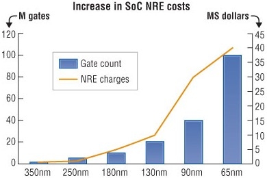
October 26, 2009 – As the expense and risk of ASIC development have risen consistently with the advance in deep submicron technology (Figure 1), the number of design starts has dropped more than 50%, from 7,749 in 2000 to 3,196 in 2007 [1], and continues to fall [2]. The cost of a new ASIC development has become prohibitive for most products that have volumes less than 1M units per year.

The availability of ASSPs, programmable logic, CPLDs, FPGAs and MPUs with extensive peripherals has contributed to this trend by allowing system designers to substitute firmware development for hardware development; development cost and schedule are reduced by overlapping hardware and firmware design and replacing hardware build cycles with compile/test/debug cycles. FPGA design starts now exceed ASIC design starts by 30:1 [3]. This trend greatly reduces the risk and expense associated with ASIC design but fails to address the needs for lower size, weight, and power.
Click to Enlarge
Figure 1. NRE costs by process geometry (Source: Semico Research Corp.)

Integration limits

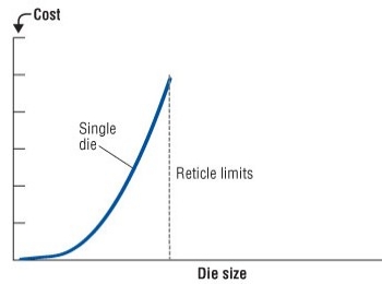
The level of integration that can be obtained in monolithic silicon has both economic and technical limitations. Advanced lithography optics don’t support die larger than approximately 28mm on a side (Figure 2, the line labeled reticle limits). The cost of a die also increases geometrically as the die size approaches the limit due to decreasing number of larger devices on a fixed area wafer and decreasing yield per device due to defect density. Also, integrating different technologies multiplies device cost by applying processing steps to device area that doesn’t require that step (e.g., by integrating DRAM into logic devices).
Click to Enlarge
Figure 2. Economic and technical integration limits

Memory bandwidth

High-speed serial interfaces are rapidly replacing parallel interfaces in large logic devices because of reduced pin counts, higher data throughput, and robustness. Supporting these higher throughputs, however, requires ever-higher memory depths and bandwidths to buffer those interfaces (Table 1).

Click to Enlarge
Table 1. Memory requirements for high-speed interfaces

The memory bandwidth required is twice the data throughput because each bit buffered must be both read and written at least once. The number of pins required is increased by 25% to approximate a 20% overhead (for example, due to refresh accesses and row precharge cycles). Large BGA packages are generally limited to about 1,900 pins because of co-planarity issues in soldering these packages to an FR-4 substrate. Higher bandwidth serial interfaces require more power and ground pins to isolate these interfaces from noise generated by other I/O pins. This then reduces the number of pins available for memory interfaces.
Click to Enlarge
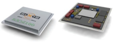
Figure 3. Embedded computing module with and without lid

SiCB technology

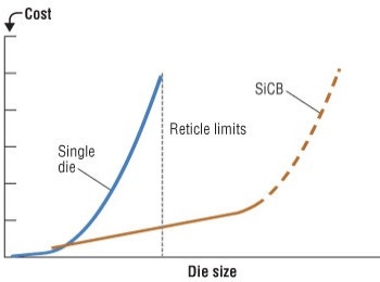
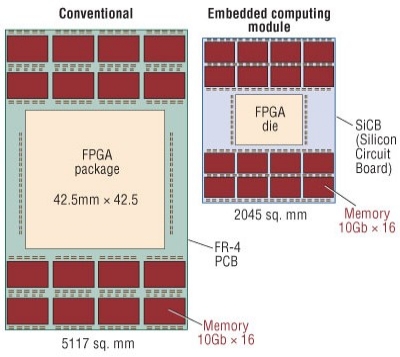
siXis Inc. develops, manufactures, and markets embedded computing modules employing SiCB (silicon circuit board) technology. A flip-chip attaches bare die devices to a large-area passive silicon substrate (Figure 3), shrinking the subsystem size by a factor of 2 to 3 (Figure 4). For instance, an FPGA can be combined with 1GB of DRAM. This level of integration will not be available in monolithic silicon for years and will be prohibitively expensive (Figure 5).

Eliminating an extra layer of packaging reduces the parasitic interconnect capacitance, reducing the module system power on the order of 22%.[4]
Click to Enlarge
Figure 4. SiCB solution for economic and technical integration limits

This approach allows integration of tested devices from different wafers fabricated in different facilities with different processes, without modification. NRE expenses for ECMs employing SiCBs are in the range of $100,000s, up to two orders-of-magnitude less expensive than SOCs. The SiCB contains only interconnect without any active devices. A complete design cycle from requirements to prototypes is on the order of 6 months. This compares favorably with SOC designs that can take 18 months or more, especially considering the risk of multiple design/fabricate/test cycles.

Since the signals connecting the devices on the SiCB are contained within the SiCB, package I/O limitations are avoided, allowing integration of large, high-speed parallel memory busses in the ECM without increasing the package I/O count beyond practical limits. This has the additional benefit of significantly reducing the complexity of the PCB to which the ECM is attached. For example, in Fig. 5, the number of signal pins soldered to the PCB is reduced 4× with an ECM.
Click to Enlarge
Figure 5. Area savings for embedded computing modules employing SiCBs

Comparison with 3D integration

3D integration of multiple semiconductor devices has been an area of active research for more than 10 years.[5] Much recent work has focused on using through silicon vias (TSVs) to stack die one on top of the other. Despite the effort expended, only one commercially available product is shipping today using TSVs (a CMOS Image Sensor (CIS) from Toshiba [6]).

A major shortcoming to this approach is thermal management. DRAMs are very sensitive to temperature and run at lower junction temperatures than high-performance logic devices, such as FPGAs or processors. Stacking memory devices on top of logic devices creates a thermal problem that is currently unsolved. Spreading the devices with SiCB integration avoids this problem.

3D stacking also requires modifying standard devices by adding TSVs, which requires detailed design information from the device manufacturer–information that is usually closely held. The siXis approach uses standard bare die with no modification. All of the new interconnect is contained in the SiCB, easing the supply chain issues associated with obtaining bare die.

Comparison with MCMs

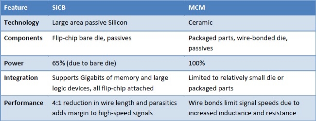
MCMs are multi-chip modules, generally built on ceramic substrates. They are limited by the feature sizes possible in ceramic technology to packaged devices or wire-bonded bare die. This limits the achievable integration and performance below the level reached by ECMs built with SiCB technology (Table 2).
Click to Enlarge
Table 2. ECM/SiCB Comparison with MCM

Conclusion

ECMS employing SiCB technology are an alternative to expensive ASIC developments, with advantages in performance and power for integrating memory and logic. They are also a practical alternative to 3D integration, which remains a technology of the future due to thermal and supply chain issues. These advantages are accompanied by a reduction in the complexity of underlying PCB designs, saving additional NRE expenses and risk, and reducing time to market.

Biography

David Blaker is vice president of engineering and manufacturing at siXis Inc., 3021 E. Cornwallis Road, Research Triangle Park, NC USA; 919-248-9193, e-mail: [email protected].


References

[1]. According to Gartner, as reported in EETimes March 26, 2007, "Sockets scant for costly ASICs"
[2]. EDN March 30, 2009, "ASIC design starts to drop 22% in 2009, Gartner reports"
[3]. Ibid.
[4]. siXis Inc., Whitepaper:  Power Savings of Embedded Computing Modules (ECMs) over FR-4 Implementations Rev. A, 8/09
[5]. "Implementation of a Gallium Arsenide Multichip Digital Circuit Operating at 500-1000 MHz Clock Rates Using a Si/Cu/SiO MCM-D Technology", IEEE Transactions on Components, Packaging, and Manufacturing Technology — Part B, Vol. 20, No. 1, February 1997, pages 17-26
[6]. SEMICON West 2009, multiple presenters

October 22, 2009 – Allvia, a specialty foundry focused on through-silicon via (TSV) technology, is expanding its manufacturing capabilities away from high-cost Silicon Valley to a newly-purchased facility in Oregon — a site with its own chip manufacturing pedigree.

The firm said the site — cryptically described as a 178,000 sq. ft. (60,000 in cleanroom space) "former semiconductor equipment manufacturing facility" in Hillsboro, OR — would be brought up to operational sometime in 2010. The company would not disclose the tooling and upgrades it is planning, nor the monetary investment it will make (and whether that includes a piece of the $5M in funding it scored back in February 2009), nor the schedule for ramping the site or eventual capacity levels.

Allvia’s current site in Sunnyvale, CA, opened in 2004 and ramped in 2007, offers TSV prototyping "and some volume production" in a far smaller ~6000 sq. ft. of cleanroom space, will be kept operational "for the foreseeable future," but eventually volume manufacturing will be "gradually" shifted north to Oregon, according to the company. Economic factors swaying Allvia to Oregon included the site’s "attractive purchase price" and cheaper operating expenses including electricity, water, and even taxes, said Allvia CEO Sergey Savastiouk, in a statement; he also noted "a tremendous talent pool of engineers and fab personnel in that community."

Some sleuthing unearths the identity of the anonymous Allvia acquisition: it’s the old ETEC Systems facility in the Evergreen Technology Center, built in 1997 and acquired by Applied Materials in 2000, and eventually shuttered in late 2005. The current owner, real estate investor Equastone, bought it from Applied in Jan. 2007. Public records indicate the site’s asking price had been lowered from $16.5M to $9.9M. The final pricetag, though, may have been as little as $5.25M — an "attractive price" indeed!

Click to Enlarge

by Debra Vogler, senior technical editor, Solid State Technology

October 20, 2009 – SST/AP sat down with IMEC’s director of interconnect and process technology unit, Bart Swinnen, to discuss the research center’s 3D program at its annual press event in Leuven, Belgium.

IMEC and its 3D integration partners have taped-out Etna, a new 3D chip integrating a commercial DRAM chip on top of its proprietary CMOS logic IC. The 3D stack resembles as close as possible, future commercial chips — it consists of a 25μm thick logic die (manufactured in its prototype line), on top of which a commercial DRAM is stacked using through-silicon vias (TSVs) and micro-bumps. One of IMEC’s 3D integration partners will deliver the DRAM dies, and will test the fabricated 3D stack; two other partners will package the 3D stack using flip-chip onto a FBGA (fine-pitch ball-grid array) substrate.

The Etna vehicle will serve production of logic die that will stack directly with a lot of commercially available memory die, according to Swinnen. "It will allow us to do a system level demonstration of the benefits of 3D," he said. "Most of this activity [until now] has been PowerPoint presentations and simulations, so this will be a real case verification."

One of the critical challenges remaining with respect to 3D implementation, according to Swinnen, is being able to provide system designers with a tool that enables smart decisions up front. "Doing 3D system integration multiplies the number of parameters that you can work with, and these parameters have to be fixed in both layers," he explained. "The system designer today has no tool, no means to enable that." Through its PathFinding tool (released in February, codeveloped with Javelin Design Automation), IMEC expects to play a role in addressing this need, providing a design tool "to not only simulate the full performance of the 3D system, but to provide an indication of what it might be with an accuracy to within 10%, so that smart choices can be made up front before the start of the design cycle," he said.

One of the 3D applications closest to market (and driving it) is stacking memory on logic to enable very high-bandwidth interface for communication between the two components, noted Swinnen. "Such an interface would very strongly outperform anything available today — there is no 2D competitor," he told SST/AP. Direct stacking of memory on memory, he added, "can justify the added cost for 3D processes." The two processes may also have different process flows, he noted. Applications for 3D stacking of high-performance computing or advanced logic will take more time to accomplish, he believes.

Aside from progress in addressing the technical challenges, Swinnen sees encouraging signs that the industry is addressing another crucial need for 3D technology: standardized definitions. "It would be very beneficial to have application specific requirement roadmaps [for 3D] that are harmonized with the ITRS roadmap," he notes.

Later this year, IMEC will release results concerning an IP block that enables communication within a 3D system. Also, at IEDM in December, IMEC will present updated research data on ring oscillator structures based upon its work disclosed at last year’s IEDM conference.

[SST/AP previously talked with Swinnen about IMEC’s 3D work at SEMICON West; click here for that video interview.]

October 16, 2009 – Taiwan’s Industrial Technology Research Institute (ITRI) will add Applied Materials to its partners for developing 3D chip stacking technology, by placing "a full line" of Applied’s tools (etch, CMP, PVD, and PECVD) in its Advanced Stacked-System Technology and Application Consortium (Ad-STAC) lab in Hsinchu, Taiwan. Their collaboration will focus on integrating via-first, via-last, and via-reveal through-silicon via (TSV) process flows.

"Joining forces with a leading research institution such as ITRI is a very effective way to advance 3D technology and successfully integrate it into the manufacturing community," said Randhir Thakur, recently appointed SVP/GM of Applied’s Silicon Systems Group, in a statement. "By performing customers’ early stage development on a proven toolset, the transition to volume manufacturing can be made as fast and transparent as possible."

ITRI — which also recently agreed to install lithography cluster and bond cluster tools from Süss MicroTec at the Ad-STAC facilities — sees 3D IC technology gain becoming "a significant part of semiconductor development" over the next decade, and thus is positioning itself to help drive 3D integration through a pilot line in its labs, noted Sheng-fu Horng, deputy general director of ITRI’s electronics and optoelectronics research laboratories. Adding AMAT’s tools to its mix of pilot technologies will help it "offer companies from different fields, as well as research institutes, a unique environment to develop and test new technologies and products."