Category Archives: 3D Integration

By Debra Vogler, senior technical editor

March 31, 2011 — Serial entrepreneur, Zvi Or-Bach, was interviewed by ElectroIQ about his latest startup, MonolithIC 3D. In this podcast interview, Or-Bach explains why the company changed its name (from NuPGA) when its mission changed. "The name change was in response to a strategic change we made once we discovered a path to monolithic 3D ICs," said Or-Bach. He noted that on-chip interconnects are the limiting aspect with respect to scaling, and that after making materials changes (i.e., Al to Cu, and SiO2 to low-k), the only solution is to go to 3D ICs.

Listen to Or-Bach’s interview:  Download (iPod/iPhone users) or Play Now

Interconnect delay → Monolithic 3D   Implant H+ dummy gates Transfer on top of processed wafer and replace gates (<400°C)
  90nm (2005) 45nm (2010) 22nm (2015) 12nm(2020)
Transistor delay 1.6ps 0.8ps 0.4ps 0.2ps
Delay of 1mm-long interconnect 5 x 10²ps 2 x 10³ps 1 x 10⁴ps 6 x 10⁴ps
Ratio 3 x 10² 3 x 10³ 4 x 104 3 x 10⁵
3D 

Figure. Next-generation monolithic 3D IC — leveraging the gate-last process. SOURCE: MonolithIC 3D

Semiconductor scaling costs

Scaling down 0.7x Scaling up (3D packaging)
 Cost: Capital >$4B  Cost: Capital: <$200M
   R&D >$1B   R&D  <$100M 
 Benefits: Die size 0.5x Benefits:  Die size 0.5x 
  Power 0.5x   Power 0.5x
Speed: No change Speed: No change

Table. The next-generation dilemma — going up or going down? Companies can do both. SOURCE: MonolithIC 3D. 

"While TSVs are a big help with off-chip interconnects, they are not helpful for on-chip interconnects — they are just too large," explained Or-Bach. "Our vertical interconnect is 10000× more dense than TSVs." The company’s mission is an answer to what Or-Bach calls the next-generation dilemma (table). Whether one chooses to continue to scale down 0.7×, or scale "up" by going to 3D, there are costs. However, the company’s estimates show a glaring difference: capital costs and R&D costs are, respectively, >$4B and >$1B for scaling down; and <$200M and <$100M for scaling up.

3D IC technology

The technology being proposed by Or-Bach uses a combination of four ideas:
1) the gate-last process and proper sequencing of ion-cut (i.e., Smart Cut) technology;
2) low-temperature face-up layer transfer;
3) repeating layouts;
4) innovative alignment.

Or-Bach explains the process in detail (figure) in his audio interview. The technology still requires process development work, but looking ahead, Or-Bach views it as being applicable to both Tier 2 fabs that want to reinvent themselves and compete with leading-edge fabs, and leading-edge fabs that want to add value.

Subscribe to Solid State Technology/Advanced Packaging.

Follow Advanced Packaging on Twitter.com by clicking www.twitter.com/advpackaging. Or join our Facebook group

By Debra Vogler, senior technical editor

March 30, 2011 — In a podcast interview recorded after SEMATECH’s workshop on design for reliability, stress management for 3D ICs using TSVs (3/17/11; Santa Clara, CA), Larry Smith, manager of SEMATECH’s 3D Enablement Center, summarizes the presentations and findings at the event. "Management of mechanical stresses is one of the key enablers for the successful implementation of 3D integrated circuits using through-silicon vias (TSVs)," Smith told ElectroIQ. "Copper-filled TSVs and wafers thinned to a few tens of microns modify the stress profiles in the silicon, and may exacerbate the stresses introduced by tier-to-tier bonding and chip-package interactions." Because these stresses have the potential to modify device characteristics, they could affect functional and parametric yield and reliability. "The stress-related impact of the processing done at the various companies in the manufacturing supply chain needs to be characterized and shared, and designers need a DFM-like solution for managing stress." Also read: TSV can deal with stress, says Synopsys

Not all efforts are directed at process challenges, however; much attention is directed at business challenges. "Concern revolves around which entity will be doing the 3D portion of a manufacturing process: the foundry, the OSAT, or the memory supplier," explained Smith. "Depending on where it gets done, that changes the critical interfaces and the standards that will be needed." Furthermore, ownership of any bad parts has to be resolved.

Smith noted that it’s commonly recognized that there is not yet a lot of manufacturing experience with respect to 3D, so the industry as a whole does not have a lot of confidence on prioritizing the failure mechanisms. "Copper pumping, or extrusions, are a concern with TSVs, and though there have been presentations with solutions," said Smith, "there is still concern as to whether or not all the issues are truly understood and really solved." Some of those outstanding issues include integrity of the liner and barrier around a TSV, along with delamination at the interfaces. A second major issue is the use of very thin die and the stresses that come with micro bumping, and so forth. And there are still questions with respect to warpage, coplanarity, and die strength. Smith further commented that while some have talked about optimizing the copper plating process and annealing, little in the way of specifics have been revealed.

"The application that the industry is focusing on now [for high-volume manufacturing (HVM)] is wide I/O DRAM for mobile applications," said Smith. "The timeline for this to be ready for HVM is by the end of 2013." He thinks it’s a good application driver for 3D; yet another application for 3D is combining processor and memory for high-performance servers. "Right now, the real need is for standards (design and modeling and EDA tools, equipment, handling, inspection/metrology, reliability test methods, etc.)." Standards will be tackled by SEMATECH’s 3D Enablement Center.

In the podcast interview, Smith also discussed accomplishments with respect to modeling — linking last year’s workshop (in total, there have been four SEMATECH workshops about this topic) with this year’s presentations.

Progress to-date:
1) Consensus on the methodology and approach (classic FEA for packaging, SNPS FEA for feature level modeling, and compact model for chip level modeling);
2) Consensus for material characteristics required;
3) Consensus for characterization techniques required for the material characteristics;
4) Several teams are considering how to interface some of the modeling tools; and
5) In terms of behavior, a compact modeling approach verified vs. classic FEA.


Listen to the podcast:  Download (iPod/iPhone users) or Play Now


Subscribe to Solid State Technology/Advanced Packaging.

Follow Advanced Packaging on Twitter.com by clicking www.twitter.com/advpackaging. Or join our Facebook group


By Debra Vogler, senior technical editor

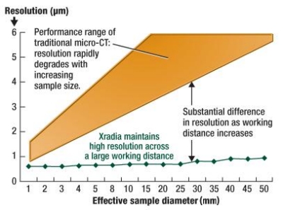
March 29, 2011 — Xradia has unveiled its latest micro computed tomography (CT) 3D X-ray imaging system, the VersaXRM, targeting gaps in the semiconductor, materials science, geomaterials, and life sciences market segments. Kevin Fahey, PhD, VP of marketing at Xradia, told ElectroIQ that the new system is able to provide a large working distance (i.e., the distance between the source spot and rotation axis of the sample) at high resolution (non-destructive).

Click to Enlarge
Figure 1. Maintaining resolution across a large working distance. Source: Xradia.

Xradia says that the system can handle a >10× larger sample size for imaging at the same resolution as conventional systems. Large working distances are important to these market segments as they enable in-situ study using environmental chambers or load cells as well as study under varying environmental conditions.

Complex 3D packaging has generated an additional class of defects that come about because of the new solder and dielectric materials, and geometries (e.g., sub-micron voids and cracks). These defects are difficult to detect inside an intact package.

Listen to Fahey’s interview: Download (iPod/iPhone users) or Play Now

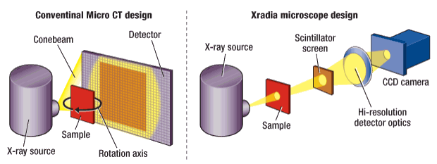
In this podcast interview, Fahey discusses how the new platform uses geometrical magnification in tandem with an X-ray microscope. Conventional microCT systems use only geometric magnification technology. By coupling geometrical magnification and optical magnification, "the combination gives very high resolution and allows the sample to sit in an environment where it is not overly sensitive to position away from the source, so we can use larger samples, or larger source-to-sample distances while maintaining high resolution," said Fahey. Modest geometrical magnification (small cone angle) works in tandem with high optical magnification.

Click to Enlarge
Figure 2. Resolution working distance benefits of microscope design. Source: Xradia.

There are many different elements that contribute to resolution: a combination of spot size of the source, the geometry of the system, the resolution of the camera, the scintillator material, vibrations in the system, any thermal variance, and so forth. "Because it’s difficult to test and specify resolution, it’s common place to focus on one of these elements as the dominant factor," noted Fahey. Conventional geometric projection systems tend to be overly sensitive to spot size, called spot blurring (fringes around the sample), explained Fahey. In comparison, the new system is not sensitive to spot size, which means larger spot sizes can be used. In turn, this means larger sources, which are inherently more stable, can be used, improving reliability.  

Click to Enlarge

Figure 3. Xradia microscope.

Fahey concludes the interview discussing throughput of a typical 3D IC package failure analysis.

Subscribe to Solid State Technology/Advanced Packaging.

Follow Solid State Technology on Twitter.com via editors Pete Singer, twitter.com/PetesTweetsPW and Debra Vogler, twitter.com/dvogler_PV_semi.

Or join our Facebook group

March 28, 2011 — Tabula Inc., a privately held fabless semiconductor company and developer of the ABAX family of 3D Programmable Logic Devices (3PLDs), secured $108 million in Series D funding. Tabula will use the new capital to accelerate production of their 3PLD ABAX product family, expand customer and partner support infrastructures, and further next-generation product development in the rapidly growing programmable logic sector.

The financing was led by Crosslink Capital and DAG Ventures. Existing investors, Balderton Capital, Benchmark Capital, Greylock Partners, Integral Capital, and NEA also participated in this round.

"The programmable logic market is seeing tremendous growth driven by the build out of the telecommunications infrastructure. This infrastructure build is necessary to keep pace with the global demand for more bandwidth to support smartphone usage for accessing data and video online," said Dennis Segers, CEO of Tabula. He said the company will increase volume shipments of its ABAX 3PLD product family and use the Spacetime architecture to integrate programmable devices into new application spaces. Tabula’s 3D programmable logic devices are high-capability programmable chips made in production volumes.

"Tabula’s Spacetime technology addresses the problems at the heart of the programmable logic market today by delivering unprecedented capabilities at unmatched cost points compared to FPGAs," said Gary Hromadko, Venture Partner of Crosslink Capital. "Tabula is well positioned to capitalize on the growing migration of ASIC and ASSP towards programmable logic devices," added Dave Strohm, Partner of Greylock Partners.

Tabula recently completed the roll-out of its 40nm ABAX family of 3PLDs supported by the Stylus development software. Stylus delivers Spacetime’s 3D Architecture price/performance advantages to ASIC and FPGA designers, maintaining a familiar design flow. Available in the cloud, Stylus eliminates IT issues while enabling real-time, on-site-like, technical support.

"Tabula has an unbounded $70B market opportunity," said Bruce Dunlevie, General Partner of Benchmark Capital.

Tabula is a privately held fabless semiconductor company developing 3D Programmable Logic Devices. Its ABAX family of 3PLDs, based on Tabula’s patented Spacetime architecture, and supported by its Stylus development software, sets new density, performance, and affordability benchmarks for programmable logic, memory, and signal processing. Please visit www.tabula.com.

Subscribe to Solid State Technology/Advanced Packaging.

Follow Solid State Technology on Twitter.com via editors Pete Singer, twitter.com/PetesTweetsPW and Debra Vogler, twitter.com/dvogler_PV_semi.

Or join our Facebook group

March 25, 2011 — Sonix Inc., scanning acoustic microscope designer and manufacturer, introduced its Stacked Die Imaging (SDI) enhancement (patent pending), which effectively inspects for defects in semiconductor stacked die and wafer level packages (WLP).

When using ultrasonic inspection to identify defects (cracks, voids, delaminations) in 3D semiconductor architectures (stacked die packages, bonded wafers), the ultrasonic signal is attenuated through each successive layer of the package or wafer, resulting in poor image quality and less accurate defect identification. Current techniques to deal with this limitation include increasing the signal gain to inspect the deeper interfaces — which saturates the images at the shallower interfaces — or changing focal position and performing multiple scans, which requires more time and limits throughput.

Sonix SDI allows users to selectively increase the ultrasonic signal gain for those interfaces of interest deeper in a semiconductor package or wafer, without saturating the shallower interfaces, providing accurate, single-scan defect identification. It also allows users to more effectively use the higher-frequency transducers required to inspect thinner die and wafers, which have less starting signal strength. Sonix SDI suits inspection of stacked die packages, lidded flip chips, and bonded wafers.

The Sonix SDI is configured through Sonix WinIC software using a simple graphical user interface (GUI) to easily select the interface of interest and the amount of signal gain to be applied. The GUI allows customers to precisely configure the gain for the entire signal profile.

Sonix SDI is available as an option on Echo, Echo VS, Echo Pro and AutoWafer tools, and as a field retrofit on all Sonix Fusion and Vision tools.

Sonix Inc. is a designer, developer, and manufacturer of scanning acoustic microscopes (SAM) for use in FA/QA laboratories, R&D, and as part of the production process. All Sonix systems have the CE Mark and are Semi S2/S8 compliant. For more information, visit www.sonix.com

Subscribe to Solid State Technology/Advanced Packaging.

Follow Advanced Packaging on Twitter.com by clicking www.twitter.com/advpackaging. Or join our Facebook group
by Dr. Phil Garrou, contributing editor

March 22, 2011 – The recent IMAPS Global Business Council (GBC) Meeting and Device Packaging Conference (DPC) was the source of some significant new developments in the areas of 3D IC and fan-out wafer-level packaging.

Matt Nowak, senior director at Qualcomm, reviewed the key attributes of 3D ICs, including performance enhancement, improved power efficiency, form factor miniaturization, and cost reduction. From there, a question arises — can 3D ICs can take the place of scaling as CMOS technology appears to be slowing (or stalling)? He concludes:

  • Yes — if performance enhancement and power reduction are the primary motivation.
  • Yes — if form factor miniaturization is the only motivation.
  • No — if cost reduction is the primary motivation. (However, 3D with TSVs can provide cost reduction benefits, if cost improvements derived from CMOS scaling diminish in future nodes, e.g. due to advanced lithography and FEOL costs.)

Sitaram Arkalgud, director of SEMATECH’s 3D IC program, shared the organization’s perspective on the readiness of 3D IC toolsets:

Click to Enlarge

Taiji Sakai of Fujitsu indicated that the demand for tighter-pitch bonding has moved the industry to copper pillar bumping but that the time/temp bonding requirements of direct Cu-Cu bonding is keeping companies from moving to that technology despite its electrical performance advantages.

Click to Enlarge

He revealed that if the Cu bumps are planarized by cutting with a diamond bit vs. the normal CMP process, a "amorphous-like layer" is produced at the surface which allows Cu-Cu direct bonding at 200-250°C (30min) vs. the >350°C (30min) required for a CMP’ed surface.

Paul Siblerud of Applied Materials announced that EMCD 3D consortium members, having met their goal of $150/wafer, will be ending the consortium this coming summer.

Rumors going around at this years IMAPS-DPC were concerned with interposers reportedly failing in thermal cycling (TC) reliability tests. Reports are that when the interposers are populated with unequal size or thickness silicon chips or chip stacks, the stresses generated on the interposers during TC causes the interposers to break. Ron Huemoeller, VP of 3D packaging for Amkor, confirmed that this indeed was an issue, but that Amkor had been able to engineer around it. He also revealed that the underfill process for the Xilinx program took more than a year get to a reliable, manufacturable state.

At the GBC, Suresh Ramalingam of Xilinx discussed their stacked silicon interconnect technology (SSIT). The 28nm Virtex-7 SSIT will reportedly use TSMC fabricated 100μm thick silicon interposers with 10-12μm Cu TSV and 65nm interconnect. The micro-bumps are Cu-SnAg alloys at 45μm pitch.

Click to Enlarge

Amkor’s Huemoeller also offered the following roadmap for memory stack usage:

Click to Enlarge

During an excellent panel session on fan-out packaging, Thorsten Meyer, one of the developers of the Infineon eWLB fan-out technology, informed the audience that his group was now part of the "Intel Mobile Communications" division, but that Infineon retains rights to non-wireless applications.

Navjot Chhabra, director of advanced packaging for the Freescale RCP fan-out program, indicated that they are in qualifications with "industrial and automotive products."

Tom Strothman, director of business development for STATS ChipPAC, indicated that eWLB is today less costly than FcBGA.

While STATS is currently running a 300mm line for production of eWLB, John Hunt, director of engineering for ASE, commented that "demand just does not warrant putting 300mm capacity in place." It was revealed that Infineon is the only commercial customer for eWLB today, with ST Micro being very close.

While all of the eWLB licensees are proposing fan-out packaging on panels, Hunt commented that ASE was "the only company who has tried to do this […] I can tell you that if we move forward with this approach it will require a totally new materials set." He indicated that they are attempting this work on 1/4 panels, not full PWB panels, and that obviously they cannot use molded underfill (MUF) to encapsulate the large substrates.


Dr. Phil Garrou is an IEEE Fellow and consultant with Microelectronic Consultants of NC.

By Debra Vogler, senior technical editor

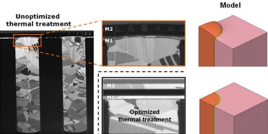
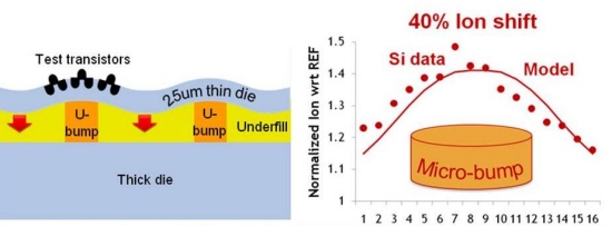
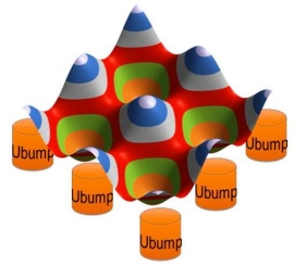
March 21, 2011 — Speaking at the SEMATECH Design for Reliability Workshop: Stress Management for 3D ICs using TSVs (March 17, Santa Clara, CA), Victor Moroz, a scientist at Synopsys, presented results of the company’s collaboration with imec (e.g., Figs. 1-3).

Listen to Moroz’s interview:  Download (iPhone/iPod users) or Play Now

In a podcast interview, Moroz explained that there are some strong effects due to stress that cannot be neglected, but taking these effects into account is doable. "Due to the mismatch between copper and silicon, the stress is not that high (100s of megapascals) — it’s lower than what you intentionally put there using stress engineering," he said.

Click to Enlarge

Figure 1. Copper pumping effect: Un-optimized TSV process leads to excessive copper pumping and destroys interconnects around it. Optimized TSV process is demonstrated to not disturb M1 and M2 interconnect layers. SOURCE: Synopsys

The difference with through silicon vias (TSVs) is that the "stress range is comparable to the size of the TSV." He noted, for example, that if a TSV is 40µm deep, then the stress range is comparable, i.e., tens of microns. "What we found is that for analog transistors, we see a change of up to 5%, and for digital transistors a change by up to 20-30% next to the TSV."

 Click to Enlarge

Figure 2. Micro-bump stress effect: The underfill shrinks considerably and pulls the thin die along in between the rigid copper micro-bumps. The thin die warps around the micro-bumps and strains the transistors. Test NFETs on top of the micro-bump exhibit 40% higher current compared to the reference NFETs that are far from micro-bumps. SOURCE: Synopsys

He added that the stress effect decays very slowly for analog transistors; the keep out zone can be tens of microns. For digital transistors, however, the effect is stronger, but it acts over a shorter range. Still, Moroz noted that these effects are not showstoppers.

 Click to Enlarge
Figure 3. Calculated warping of the thin die (vertical scale exaggerated). Thin die goes up above the Cu micro-bumps, forming hills there, with valleys and saddles in between the micro-bumps.  The Si-calibrated model can be used to account for TSV and micro-bump stress effects and design reliable 3D ICs. SOURCE: Synopsys

Subscribe to Solid State Technology/Advanced Packaging.

Follow Advanced Packaging on Twitter.com by clicking www.twitter.com/advpackaging. Or join our Facebook group<

March 21, 2011 — CEA-Leti and IPDiA have formed a common lab to capitalize on their complementary expertise in miniaturization and 3D integration on silicon.

The common lab is dedicated to developing new 3D-integration technologies for passive electronics components on silicon, targeting new applications in LED lighting, healthcare and aerospace that require extreme miniaturization. The partnership also will aim for improved miniaturization of passive components such as resistors, capacitors and inductors.

The common lab will develop very high-end passive components on silicon that will resist harsh environments, functional sub-mounts for lighting components, and assembly technologies that enable ultra-miniaturization of future products.

IPDiA was founded to commercialize innovative 3D technologies for integrating passive components. The company’s two axes of focus are integrated devices for high-brightness LEDs (HB-LEDs) and integrated passive devices (IPDs) for new medical, industrial, aerospace and defense markets.

CEA-Leti’s expertise in 3D technologies will allow IPDiA to go beyond the third generation of Passive Integration Connecting Substrate (PICS) components (250nF/mm2), which are being produced at IPDiA’s Caen site, and pursue the development of a future generation of PICS components (1µF/mm2, then 2µF/mm2) and their assembly. These products are designed, developed and manufactured by IPDiA in its production unit.

Franck Murray, CEO of IPDIA, pointed out that the Common Lab will entail "common work between teams from various backgrounds generating creativity and new ideas."

CEA-Leti and IPDIA have worked together since IPDIA formed in 2009.

CEA is a French research and technology organization, with activities in four main areas: energy, information technologies, healthcare technologies and defense and security. Within CEA, the Laboratory for Electronics & Information Technology (CEA-Leti) works with companies in order to increase their competitiveness through technological innovation and transfers. CEA-Leti is focused on micro and nanotechnologies. Visit www.leti.fr.

IPDiA is a leader in passive-components integration on silicon with a global offer for miniaturization that features high-level technological and economic performance. The company is mainly focused on healthcare, lighting, communication, defense, aerospace, industry and automotive. For more information, visit www.ipdia.com.

Subscribe to Solid State Technology/Advanced Packaging.

Follow Advanced Packaging on Twitter.com by clicking www.twitter.com/advpackaging. Or join our Facebook group