Category Archives: 3D Integration

by Dr. Phil Garrou, contributing editor

March 18, 2011 – At the recent CeBIT Fair in Hanover, Germany, IBM CEO Sam Palmisano announced that IBM’s 3D technology will likely appear in its Power8 processor, planned for 2013, using 28nm or 22nm process technology.

The first goal, he indicated, is to place the memory directly above or beneath the CPU. The processor will likely employ a linked memory and "a layer of small specialized computing cores adapted for specific intended uses." Future plans envision up to 100,000 connections per mm2 in silicon.

The principal issue with 3D ICs for processor units is cooling. IBM has undertaken 3D stack cooling research with the École Polytechnique Federale and ETH Zurich. At the CeBIT fair, IBM scientists presented the first test chips in which cooling water is circulated through 50µm channels (i.e microchannel cooling). Bruno Michel, manager of the Advanced Thermal Packaging group at IBM Research Zurich, reported that the energy-efficient hot water-cooling technology is part of their concept of a zero-emission data center. 3D chip stacks which generate more heat than a single processor, in almost the same amount of space, are cooled using water and not air to reduce energy consumption. IBM reports that it will be a few more years before this technology is ready for production.

March 17, 2011Applied Materials Inc. (AMAT) introduced the Applied Centura Conforma, with conformal plasma doping (CPD) targeted for 22nm and beyond logic and memory chips. The technology replaces ion beam implantation for conformal doping of complex 3D structures.

Click to EnlargeThe Conforma system combines high-dose, low-energy doping technology with in-situ clean capability in a single vacuum chamber to deliver uniform, high throughput doping on both planar and 3D structures. The system uses a pure, additive-free doping chemistry that preserves the underlying device structures.

The plasma doping technology draws from AMAT technologies for RF engineering and CVD chamber design, said Sundar Ramamurthy, vice president and general manager of the Front End Products business unit at Applied Materials, adding that Conforma systems are running in customers’ pilot and high-volume manufacturing. "We’re also working with customers and research entities on pioneering R&D programs using our proprietary technology."

Doping is traditionally performed by bombarding the wafer with a beam of dopant ions moving at high speed. However, this straight line bombardment process cannot provide uniform doping of advanced three-dimensional structures. More importantly, the fast-moving ions can damage the ultra-thin semiconductor layers in cutting-edge chips. Applied’s Conforma technology provides a gentle, low-energy process that enables uniform, conformal doping over complex 3D chip structures. The Centura Conforma combines integrated plasma pre-clean and RTP anneal on the same vacuum platform.

Some of the advanced devices enabled by the new Conforma system include finFET logic, vertical gate DRAM and vertical NAND flash memory arrays.

Applied Materials, Inc. (Nasdaq:AMAT) provides equipment, services and software to enable the manufacture of advanced semiconductor, flat panel display and solar photovoltaic products. Learn more at www.appliedmaterials.com.

Subscribe to Solid State Technology/Advanced Packaging.

Follow Solid State Technology on Twitter.com via editors Pete Singer, twitter.com/PetesTweetsPW and Debra Vogler, twitter.com/dvogler_PV_semi.

Or join our Facebook group

March 15, 2011 — TeraView, provider of terahertz solutions and technology, is collaborating with the Hyperspectral Engine Lab for Integrated Optical Systems (HELIOS) in a Third-Frontier-supported project within the Electrical Engineering Department of Ohio State University (Columbus, OH). Headed by Professor J. Volakis, HELIOS aims help turn technology into commercial solutions–in this case, to improve semiconductor package failure analysis using terahertz technology.

As part of the collaboration TeraView has provided one of its Electro Optical Terahertz Pulsed Reflectometry (EOTPR) systems. These units were originally developed with Intel and are used for isolating faults in advanced 3D semiconductor packages. This is the first time the technology has been made available outside of Intel and it is hoped to use the unit to expose the technology to a wider North American semiconductor audience. The EOTPR system provides an alternative use of terahertz signals. Electrical pulses containing frequency components in the terahertz region are generated and able to propagate through interconnects in semiconductor packages allowing greatly improved fault isolation.

TeraView is investigating setting up a US office in the region, with the EOTPR system exposure to a Noth American audience, said Don Arnone, Teraview CEO.

A spin out from Toshiba and Cambridge University in 2001 and employing 25 staff, Teraview has been developing terahertz technology for medical imaging, electronics, defense and security, non-destructive testing, and pharmaceuticals. Learn more at www.teraview.com

March 9, 2011 – BUSINESS WIRE — SEMATECH experts reported new breakthroughs in wafer bonding at the 7th Annual IMAPS Device Packaging Conference (DPC), March 7-10 in Scottsdale, AZ. Low-temp die tacking has yielded faster die-to-wafer integration.

Technologists from SEMATECH’s 3D Interconnect program have demonstrated a novel die-to-wafer interconnect process using a die-tacking and collective-bonding approach on a 300mm wafer platform for 3D-IC applications. Composite wafers containing a 50µm thin through-silicon-via (TSV) wafer attached to a supporting handle wafer were populated with die using a short, low-temperature tacking process. This process enables a faster method of die-to-wafer integration needed for the advancement of heterogeneous 3D-ICs.

Wafer-to-wafer (WtW) bonding is a key enabling process step for 3D interconnection of wafers through stacking. The International Technology Roadmap for Semiconductors (ITRS) roadmap for high density, intermediate level, TSVs specifies via diameters of 0.8 to 4.0µm in 2012 and beyond.

3D ICs will play an important role in the semiconductor industry, given their potential to alleviate scaling limitations, increase performance and functionality, and reduce cost. New and improved technologies and integration schemes will be necessary to realize 3D’s potential as a manufacturable and affordable path to sustaining semiconductor productivity growth.

Additionally, Sitaram Arkalgud presented a summary of SEMATECH’s programs in 3D IC technology development and emerging standards at the Global Business Council Spring Conference, held in conjunction with DPC. Arkalgud delivered an invited talk highlighting SEMATECH’s 3D Enablement program and a summary on how it will enable industry-wide ecosystem readiness for cost-effective TSV-based stacked IC solutions.

SEMATECH’s 3D program was established at CNSE’s Albany NanoTech Complex to deliver robust 300mm equipment and process technology solutions for high-volume TSV manufacturing. SEMATECH established the 3D Enablement program to drive cohesive industry standardization efforts and technical specifications for heterogeneous 3D integration. Administered by SEMATECH’s 3D Interconnect program, in partnership with SIA and SRC, the program is developing technologies and specifications necessary for establishing standards in critical areas such as inspection, metrology, microbumping, bonding and thin wafer and die handling. SEMATECH is an international consortium of leading semiconductor manufacturers. Learn more at www.sematech.org

More news from IMAPS Device Packaging:

Subscribe to Solid State Technology/Advanced Packaging.

Follow Advanced Packaging on Twitter.com by clicking www.twitter.com/advpackaging. Or join our Facebook group

March 9, 2011 – Business Wire — Hynix Semiconductor Inc. (Hynix), DRAM and flash memory supplier, has become a member of SEMATECH’s 3D Interconnect program at the College of Nanoscale Science and Engineering (CNSE) of the University at Albany.

Hynix will collaborate with engineers in SEMATECH’s 3D Interconnect program at CNSE’s Albany NanoTech Complex to address industry infrastructure and technology gaps in materials, equipment, integration and product-related issues for high-volume adoption of through silicon vias (TSV). Through technology leadership and global collaboration, SEMATECH’s 3D Interconnect program emphasis is on exploring 3D technology options that provide cost-effective and reliable solutions to drive manufacturing readiness of 3D TSV.

Volume implementation of wide input/output (I/O) memory-based products is gaining significant momentum in the microelectronics industry. Worldwide academic and industrial research activities are currently focusing on stacked wide I/O DRAM for mobile applications. Successful deployment of wide I/O and TSV combination will enable heterogeneous 3D integration and volume production of 3D-based packages. Hynix and SEMATECH will address commercialization challenges and wide I/O interface structures using TSVs for high-volume manufacturing within the next two years.

"3D integration offers a path for higher performance, higher density, higher functionality, smaller form factor, and potential cost reduction," said Dr. Sung Joo Hong, head of the R&D division of Hynix Semiconductor, adding that the goal in SEMATECH’s 3D Interconnect program is realizing 3D’s manufacturability and affordability potential. To acheive high-volume manufacturing (HVM) by 2013, industry-wide cooperation is neccessary, said Raj Jammy, vice president of emerging technologies at SEMATECH.

Hynix Semiconductor Inc. (HSI) is a top-tier memory semiconductor supplier offering Dynamic Random Access Memory chips (DRAMs), Flash memory chips (NAND Flash) and CMOS Image Sensors (CIS). The company’s shares are traded on the Korea Exchange, and the Global Depository shares are listed on the Luxembourg Stock Exchange. Further information about Hynix is available at www.hynix.com

SEMATECH is an international consortium of leading semiconductor manufacturers. Learn more at www.sematech.org

The UAlbany CNSE is dedicated to education, research, development, and deployment in the emerging disciplines of nanoscience, nanoengineering, nanobioscience, and nanoeconomics. With over $7 billion in high-tech investments, the 800,000-square-foot UAlbany NanoCollege houses a fully integrated, 300mm wafer pilot prototyping and demonstration line within 80,000 square feet of Class 1 capable cleanrooms. More than 2,500 scientists, researchers, engineers, students, and faculty work on site at CNSE’s Albany NanoTech, from companies including IBM, GlobalFoundries, SEMATECH, Toshiba, Samsung, Applied Materials, Tokyo Electron, ASML, Novellus Systems, Vistec Lithography and Atotech.

An expansion currently in the planning stages is projected to increase the size of CNSE’s Albany NanoTech Complex to over 1,250,000 square feet of next-generation infrastructure housing over 105,000 square feet of Class 1 capable cleanrooms and more than 3,750 scientists, researchers and engineers from CNSE and global corporations. For more information, visit www.cnse.albany.edu

Subscribe to Solid State Technology/Advanced Packaging.

Follow Advanced Packaging on Twitter.com by clicking www.twitter.com/advpackaging. Or join our Facebook group
March 8, 2011 – BUSINESS WIRE — Optomec Aerosol Jet product manager Mike O’Reilly will give a presentation titled "Aerosol Jet Printing as an Alternative to Wire Bond and TSV Technology for 3D Interconnect Applications" at the IMAPS (International Microelectronics and Packaging Society) Device Packaging Conference on March 9.

O’Reilly will discuss how, based on cost and functional advantages, the Aerosol Jet process is emerging as an effective alternative to traditional wire bond and through-silicon-via (TSV) technologies. Aerosol Jet systems have high-density 3D interconnect capabilities that enable multi-functional integrated circuits (ICs) to be stacked and vertically interconnected in high-performance system-in-package (SiP) devices. The die stacks can include 8 or more die, with a total stack height of ~1mm.

The printing system has a working distance of several millimeters, which means that no Z-height adjustments are required for the interconnect printing. Closely coupled pneumatic atomizers with multiplexed print nozzles are used to achieve production throughput of greater than >18,000 interconnects per hour, and high aspect ratio interconnects with 30µm line width and 6µm line heights have been demonstrated at sub 60µm pitches with low resistivity.

The presentation will also include pre-production qualification results, final production packaging, and further definition of the Aerosol Jet print platform integrated within a high throughput, manufacturing ready automation solution.

The IMAPS Device Packaging conference is being held March 8-10th at the Radisson Fort McDowell Resort and Casino in Scottsdale/Fountain Hills, Arizona. The seventh Annual Device Packaging Conference is an international event and attracts a diverse group of people within industry and academia. It provides a chance for educational interactions across many different functional groups and experience levels. The conference provides a focused forum on the latest technological developments in five topical workshop areas related to microelectronic packaging, including 3D IC & Packaging, Flip Chip Technologies, MEMS & Associated Microsystems, Wafer Level Packaging; and Emerging Technologies (LEDs & Passive Integration).

Optomec provides additive manufacturing technologies for high-performance applications in the electronics, solar, medical, and aerospace & defense markets. Learn more at www.optomec.com

Subscribe to Solid State Technology/Advanced Packaging.

Follow Advanced Packaging on Twitter.com by clicking www.twitter.com/advpackaging. Or join our Facebook group

March 3, 2011 – Marketwire — Cascade Microtech Inc. (NASDAQ: CSCD) and imec entered into a collaborative research partnership for testing and characterization of 3D integrated circuit (IC) test structures. Imec will work closely with Cascade Microtech to develop test methods and methodologies for emerging 3D through silicon via (TSV) structures, and to lead the way in development of global standards for 3D IC development and production test.

3D-TSV stacked ICs, still an emerging technology, allow multiple chips to be stacked and integrated into a single package, reducing the form factor and power consumption and increasing the bandwidth of inter-chip communication by eliminating connections through the circuit board for mobile advanced devices like tablets and smartphones. Chip stacking with 3D-TSV interconnects requires known good die (KGD) wafer probing with high test coverage before stacking to achieve practical stack yields. The high density of TSV interconnects has challenged conventional probe card architectures, limiting electrical test access.

The complexities of test inherent in new 3D TSV integrated circuit designs will be a key focus of the research project that will take place at imec’s research facilities in Belgium, where silicon wafers with test probe structures of 40µm pitch and smaller will be manufactured and tested. In the process of ongoing research, imec will install the first turnkey 3D test solution comprising of a 3D-TSV probe station and a new probe card from Cascade Microtech. The probe station and probe cards will be used to characterize the TSVs in the chip stacks as part of ongoing efforts to optimize 3D stacked integrated circuit performance and reliability.

"The collaboration with Cascade Microtech in this early phase of engineering and development will enable us to identify challenges and provide solutions for test issues that are specific for 3D integrated systems. Enabling probing solutions for high-density interfaces, minimizing the impact of pre-bond testing on stacking yield and test access to buried layers are key challenges for testing 3D systems that we will address through this collaboration," said Erik Jan Marinissen, imec principal scientist. "The complexity of the 3D-system supply chain is reflected in the partner portfolio of imec’s 3D research program, where leading IDMs, foundries, fabless companies, outsourced semiconductor assembly and test providers (OSATs), equipment and material suppliers, as well as EDA companies partner to develop and improve 3D technologies. A good alignment of these multi-disciplinary forces is required to make 3D system integration an industrial reality." 

"Ongoing research is critical for Cascade Microtech’s 3D TSV solution path, and imec is a key collaboration partner for our development efforts, given its history of successful research collaboration, its superior research facilities, its commitment to the semiconductor industry and the expertise of its staff," said Michael Burger, president and CEO, Cascade Microtech, Inc. "In recent years, probing and test were viewed as a major barrier to 3D TSV development and manufacturing. We are looking forward to breaking through the barrier, paving the way for our mutual customers to quickly achieve extremely cost-effective 3D TSV test solutions."

Imec performs world-leading research in nanoelectronics. Further information on Imec can be found at www.imec.be.

Cascade Microtech, Inc. (NASDAQ: CSCD) is a leader in the precise electrical and mechanical measurement and test of integrated circuits (ICs) and other small structures. For more information, visit www.cascademicrotech.com.

Subscribe to Solid State Technology/Advanced Packaging.

Follow Advanced Packaging on Twitter.com by clicking www.twitter.com/advpackaging. Or join our Facebook group

March 3, 2011 — NuPGA Corporation has changed its name to MonolithIC 3D Inc. The company incorporated in 2009 with the mission to develop better programmable logic technology with density, speed, and power approaching ASICs. As it developed an improved FPGA technology, the NuPGA team discovered a path for practical monolithic 3D ICs. MonolithIC 3D Inc. changed its strategy to focus on monolithic 3D IC technology as a pure IP innovator organization.

MonolithIC 3D’s patented technologies offer chipmakers an economical and efficient way to create semiconductor chips in vertical "stacks" of circuit elements that delivers vertical connectivity 10,000 times better than the existing TSV-based 3D stacking. The company’s technologies have the potential to increase semiconductor device speed, lower power requirements, reduce silicon area, and be cost competitive with traditional dimensional scaling. 

MonolithIC 3D has filed more than 30 fundamental patent applications that cover the basic technology as well as significant applications of 3D IC technology.

"MonolithIC 3D’s technology can enable older fabs to use 3D IC to successfully compete in the mobile market. My hope is that by empowering the older process nodes to create better devices and products, we can reverse the NRE cost trend and ignite the ASIC market and device innovation," noted Zvi Or-Bach, founder of MonolithIC 3D.

The MonolithIC 3D team consists of semiconductor and semiconductor equipment industry veterans with deep experience in design innovation and collaborates with researchers at Stanford University, Rice University, and other research organizations. Learn more at www.MonolithIC3D.com

Subscribe to Solid State Technology/Advanced Packaging.

Follow Advanced Packaging on Twitter.com by clicking www.twitter.com/advpackaging. Or join our Facebook group

by Dr. Phil Garrou, contributing editor

February 27, 2011 – Samsung — who in December 2010 announced 40nm 8GB RDIMM based on 4Gb, 1.5V, 40nm DDR3 memory chips operating at 1,333MHz and 3D TSV chip stacking architecture for servers applications — announced at the International Solid-State Circuits Conference (ISSCC, Feb. 20-24 in San Francisco) the development of wide I/O 1Gb DRAM for mobile applications like smartphones and tablet computers. The 3D TSV architecture will be implemented in their 50nm node DRAM technology.

Previous generations of mobile DRAM, low-power DDR2 DRAM (LPDDR2) which runs at approximately 3.2-Gb/ sec, uses a maximum of 32 pins for I/O. The new wide I/O solution, which has 512 I/O (up to 1200 total pins), can transmit data at a rate of 12.8Gb/sec, resulting in a significant improvement in processing power. In addition it reportedly reduces the power consumption by 75%.

Following this wide I/O DRAM launch, Samsung is reportedly focusing on 20nm, 4Gb wide I/O mobile DRAM for delivery in 2013.

The 64.34mm2 is made up of 4 partitions symmetric with respect to the chip center, each partition consisting of 4×64Mb arrays, peripheral circuits and microbumps. The microbumps are 20×17μm2 on 50μm pitch. The TSVs are 7.5μm diameter with 0.22 – 0.24Ω resistance and 47.4fF capacitance.

By Debra Vogler, senior technical editor

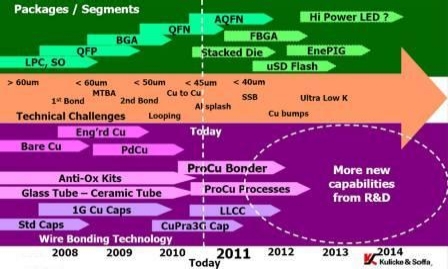
February 23, 2011 — As gold becomes more expensive, copper wire bonding becomes more appealing for chip packaging. Reverse bonding, fine-pitch bonding, looping, second bonds, and other technologies are ramping on roadmaps, according to Kulicke & Soffa (K&S).

Bob Chylak, VP engineering, packaging & process integration at Kulicke & Soffa, was the featured speaker at a recent iMAPS NorCal chapter lunch meeting (Santa Clara, CA; 2/2/11). He covered the topic of converting from gold to copper for wire bonding — a move gaining ever greater interest by the surging price of gold. With heightened activities to close the knowledge gap with respect to using copper, many of the challenges have been addressed, observed Chylak.

Listen to Chylak’s interview:  Download (iPhone/iPod users) or Play Now

Laying out his company’s copper R&D roadmap (figure), Chylak noted that high-volume production of fine-pitch copper replacing gold already started in 2010. Advanced QFNs and stacked die still need to be developed, and LED packaging needs to be transitioned to copper, though Chylak noted that the challenge there will be with copper’s reflectivity not being as good as gold.

Click to Enlarge

Figure. Copper transition and roadmap planning. SOURCE: Kulicke & Soffa

Chylak said that nearly the entire K&S process engineering staff is working on the copper transition. In particular, work is being done on reverse bonding and getting yields to 50ppm or less. "It’s mainly around the looping [for stacked dies] and second bonds [including for LEDs] we’re focusing on," said Chylak.

Subscribe to Solid State Technology/Advanced Packaging.

Follow Advanced Packaging on Twitter.com by clicking www.twitter.com/advpackaging. Or join our Facebook group