Category Archives: LED Manufacturing

by Dr. Paula Doe, SEMI Emerging & Adjacent Markets

June 29, 2011 – At $10, long life and low energy use make LED lighting costs compelling for the consumer. Despite major recent progress, however, current prices are closer to $40.

"Improvements in device efficacy have been driving big improvements in lumens per dollar, but that’s getting close to the theoretical maximum — there’s not room to double it again, but costs still need to come down much more than that," says Bryan Bolt, Cascade Microtech’s director of technology development. "So that means it’s now all about manufacturing efficiency — things like designing devices that are easy to manufacture, and improving cost-of-ownership of equipment." Better wafer-level testing is one area that can have a big impact on reducing costs by avoiding the high cost of packaging for bad die. Also key will be bringing traceability to test, for tracking defects back to root causes. But for test suppliers to deliver traceability, the sector will need to come to some degree of consistency in operating conditions and performance parameters from the wide range of different probers, spectrometers, integrating spheres, and software now put together in different combinations by individual LED makers.

Better measurement of process conditions can also improve yields. Veeco Instruments chief technologist Bill Quinn reports that test results using the near UV pyrometer developed with Sandia National Lab to monitor the temperature of the transparent and often warped sapphire wafer directly during epitaxial deposition — instead of just the temperature in the pocket in which it sits — are showing potential to improve yields even in a well-controlled manufacturing environment. With each 2

June 28, 2011 — As light-emitting diode (LED) adoption continues to grow, LED driver ICs face pressure from increased IC integration, driver-less AC-LEDs and other technologies, and falling prices. However, the driver IC unit can bring performance and power enhancements that consumers want for LED lighting adoption.

LED driver IC sales are seeing >10% compound annual growth, with a rise from nearly $2 billion in 2010 to nearly $3.5 billion in 2015 (12% CAGR), says market research group Strategies Unlimited. The driver is the entire LED circuit, including the driver IC but excluding the LEDs.  As edge-lit TV and monitor sales grow, LCD backlight LEDs will dominate. The production value of drivers for lighting will see strong 40% compound annual growth through 2015.  

The promise of an LED lighting boon is still on the horizon, and Strategies Unlimited expects replacement bulbs to eat into the incandescent bulbs

by Michael A. Fury, Techcet Group

April 26, 2011 – The MRS Spring 2011 meeting is officially open in Moscone West in San Francisco. Fifty-one technical symposia will run concurrently, with over 5000 paid attendees from 50 countries, 3100 oral papers, 1700 posters, 122 exhibitors, and 14,600 entries in the authors’ directory. This author list is comparable to the total MRS membership of ~15,100.

Click to EnlargeThe opening day of this week-long meeting (Monday 4/25) consisted of nine tutorial sessions related to specific symposia topics, and a light load of two technical symposia that were scheduled to get an early jump on the week. Tutorial topics included phase-change materials, NV RAM, compound semiconductors for energy applications, and two sessions related to PV.

A few additional fun facts: running a symposium of this nature requires 38,000 chairs. If we were standing, we probably would not need as much coffee to stay alert — the attendees will consume about 1000 gallons of coffee over five days, for which the MRS will pay the Moscone Center ~$100,000. At $100 per gallon, it is little wonder that the Moscone staff ends the coffee breaks at the appointed time with ruthless efficiency. It also puts the price of gasoline into perspective.


(Additional presentation details can be found online on the MRS Spring 2011 abstracts page. The underscored codes at the beginning of papers reviewed below refer to the symposium, session and paper number.)

OO2.3: Michael Gwinner of the U. of Cambridge presented work on novel light-emitting FETs (LEFETs) which use a 20-30nm thick film of solution processable ZnO or InZnO to lower the electron injection barrier between the Au electrodes and the poly(9,9-dioctylfluorene-alt-benzothiadiazole) (F8BT) channel. This results in an increase in two orders of magnitude in the ambipolar current, and therefore in the light intensity. A blue emitting device was similarly shown with a poly(9,9-dioctylfluorene) (F8) channel.

OO2.4: Jana Zaumseil from U. Erlangen-Nuremberg studied the effect of selectively dispersed single-walled nanotubes (SWNT) in semiconducting polyfluorenes in collaboration with the Cambridge work cited above. Charge injection into the F8BT and F8 was significantly enhanced, even at low concentrations of SWNT. The structures proposed could lead to novel optoelectronic devices operating efficiently in the near-infrared telecommunication wavelength window.

WW2.1: Darrell Schlom of Cornell has apparently found a way around the high point defect levels associated with BaxSr1-xTiO3 films that are formulated for high tunability at microwave frequencies. Such films are desired to exploit the paraelectric-to-ferroelectric transition that occurs just below ambient temperatures. Schlom found that altering layers of SrO and TiO2, with the periodic injection of a double layer of SrO, results in planar defects rather than point defects. Further, biaxial tension induced by lattice mismatch from a judicious choice of substrate results in ferroelectric films. Layering thus provides an additional degree of freedom to tune the ferroelectric properties of materials. This approach is available only to thin films, not to bulk materials. One of his layered compositions, Sr7Ti6O19, has the highest ferroelectric figure of merit of any known material.

OO3.2: Franky So from the U. of Florida fabricated a high-efficiency white OLED device by constructing a blue OLED in a tunable microcavity and capturing the emission with a red-yellow phosphor mix, and further enhancing the efficiency with a macrolens. The net effect is to convert a 68 lm/W blue structure to a 99 lm/W device with excellent white rendering.

OO3.4: N. Erickson of the U. of Minnesota demonstrated a device with a single graded organic layer that transitioned smoothly from 100% hole transmitting material at the anode to near 100% electron transmitting material and the cathode. The resulting external quantum efficiency (16.9%) and power efficiency (61 lm/W) are comparable to figures of merit for more complex multilayer structures. It was proposed that extension of the approach to red and blue emitting devices may provide a path to simple products for white electrophosphorescence.

OO4.1: E.C. Turner of Arizona State has synthesized a series of metal complexes to enhance the phosphorescence of Pt- and Pd-based emitters with Λmax in the range of 420-450nm. These materials exhibit room temperature photoluminescence efficiencies that are several orders of magnitude greater than analogous emitters. The method can be generalized to other phosphorescent complexes for enhancing their emissive properties.

WW2.8: Pankaj Sharma from the U. of Nebraska used piezoresponse force microscopy (PFM) to investigate the 3D arrangement of polarization and switching behavior of ultrathin films of poly(80% vinylidene fluoride-20% trifluoroethylene), or PVDF-TrFE. Switching studies of PVDF-TrFE nanomesas were performed as a function of bias magnitude and duration with sub-10nm spatial resolution.

OO4.6: Hans Spaeth of U. of Cincinnati reported on the operation of biopolymer-based organic light-emitting diodes (BiOLEDs) that incorporate phosphorescent emitting layers. Significant increases in brightness and efficiency have been obtained over fluorescent BiOLEDs. Natural salmon sperm DNA is one of the materials frequently used in research for photonic applications development.


Michael A. Fury, Ph.D, is senior technology analyst at
Techcet Group, LLC, P.O. Box 29, Del Mar, CA 92014; e-mail [email protected].

March 21, 2011 — The Optogan Group, Germany-based LED manufacturer, placed a multi-system order for Oxford Instruments’ etch and deposition systems. These include PlasmaPro System133 ICP and PlasmaPro 800Plus RIE etch systems, and a PlasmaPro 800Plus deposition system. 
 
The PlasmaPro System133 process tool offers up to 27 x 2" batch etch capability for GaN-on-sapphire wafers, while the PlasmaPro 800Plus tools are a flexible solution for plasma etching and deposition processes on large wafer batches of up to 43 x 2" wafers, in a compact footprint, open loading system.

The Optogan Group develops and produces high-brightness light emitting diodes (HB-LEDs) for global applications and ordered the systems for installation at its high-volume production manufacturing line in Landshut, Germany.
 
Optogan has operated an Oxford system for several years, and is now adding Oxford Instruments’ production systems for their large batch, high yield and high speed capabilities. Optogan cited high throughput, repeatability, and excellent local customer support as keys to the repeat order.

Oxford Instruments provides high technology tools and systems for industrial and research markets. It is listed on the London Stock Exchange (OXIG).

Oxford Instruments Plasma Technology offers flexible, configurable process tools and leading-edge processes for the precise, controllable and repeatable engineering of micro- and nano-structures. Its systems provide process solutions for nanometer-layer epitaxial growth of compound semiconductor material, etching of nanometer-sized features and the controlled growth of nanostructures. These solutions are based on core technologies in plasma-enhanced deposition and etch, ion-beam deposition and etch, atomic layer deposition and hydride vapor phase epitaxy.

The Optogan Group is one of the technology leaders in the manufacturing of light-emitting diodes (LEDs). Learn more at http://www.optogan.com

Subscribe to Solid State Technology/Advanced Packaging.

Follow Solid State Technology on Twitter.com via editors Pete Singer, twitter.com/PetesTweetsPW and Debra Vogler, twitter.com/dvogler_PV_semi.

Or join our Facebook group

Veeco GaN MOCVD tool debut


February 17, 2011

By Debra Vogler, senior technical editor

February 17, 2011 — Veeco Instruments’ new TurboDisc MaxBright GaN MOCVD multi-reactor system is poised to take advantage of what the company believes is an accelerated rate of LED TV penetration (Fig. 1). According to Jim Jenson, VP of marketing at Veeco, who cited DisplaySearch/Veeco estimates in a podcast interview with SST, LED TV penetration is expected to reach 50% in 2011 and increase to ~80% in 2013, or perhaps sooner. Among the reasons LEDs are replacing LCD TVs that are backlit with CCFL technology are:

  • LEDs enable much thinner TVs and lower power consumption,
  • LEDs have better display characteristics (e.g., LEDs can do local dimming in direct-lit displays),
  • LEDs do not contain mercury, as do CCFLs.

Listen to Jenson’s interview: Download (iPhone/iPod users) or Play Now

Besides LED TVs, Jenson says many LED manufacturers are already positioning themselves to take advantage of the move to replace incandescent light bulbs and fluorescent tube lighting.

Click to Enlarge
Figure 1. LED TV opportunity. SOURCES: DisplaySearch Q4/10 and Veeco estimates.

The new system targets manufacturing of high-brightness LEDs (HBLEDs) and is capable of single- or multi-chamber layer growth; this allows for LEDs to be manufactured either serially (individual layers of LEDs can be grown sequentially in each reactor) or in parallel (the entire LED is grown on a per reactor basis). Two to four different reactors can be mounted around a central handler, which can handle a higher capacity carrier, and according to Jenson, each reactor can handle 20% more wafers than the previous generation.

Click to Enlarge Click to Enlarge
Figure 2. a) Within-wafer uniformity and b) Wafer-to-wafer uniformity.

An enabling feature of the tool is model-based temperature control, which uses a proprietary close-loop thermal control algorithm. Jenson explains that conventional closed-loop thermal control uses PID technology, which has a relatively slow settling time, taking a number of minutes for the temperature to stabilize after significant excursions. The new tool uses an algorithm that creates a 3D model in time of the entire thermal environment of the reactor; it requires about 500 differential equations being solved simultaneously every time there is a temperature change. "This results in very fast transitions, and very fast settling time between one temperature change and another," said Jenson. "We see a 5-10% throughout improvement."

According to Jenson, the tool has a >90% yield in a 5nm bin which means 90% of the LEDs on a platter, or 90% of the LEDs within a wafer, are within a wavelength range of 5nm (Fig. 2).  

Subscribe to Solid State Technology/Advanced Packaging.

Follow Solid State Technology on Twitter.com via editors Pete Singer, twitter.com/PetesTweetsPW and Debra Vogler, twitter.com/dvogler_PV_semi.

Or join our Facebook group

February 11, 2011 – Marketwire — Palomar Technologies, precision microelectronics and optoelectronic packaging systems provider, will hold meetings at Stategies in Light to discuss its recent upgrades to high-brightness light emitting diode (HB-LED) assembly.

Strategies in Light will take place February 22-24 in Santa Clara, CA.

Worldwide account manager for Assembly Services, Steve Buerki, will be on site at the Strategies in Light conference at booth #238. Palomar is offering free admission passes to the Strategies in Light exhibitors’ show floor for attendees to speak with Buerki.

Precision Microelectronics Assembly Services (Assembly Services) is the contract assembly division of Palomar Technologies. Assembly Services provides prototyping, test, measurement and production for high accuracy and complex wire and die attach applications. Additional clean room space was recently added in the California-based laboratory, increasing production capacity by 50%. Assembly Services expertise includes development and production for applications such as HB LEDs, RF power modules, military hybrids and laser diode packages.

Palomar Technologies, a former subsidiary of Hughes Aircraft, provides die attach solutions, wire bonding equipment, optoelectronic packaging systems and contract assembly services. For more information, visit www.palomartechnologies.com.

Subscribe to Solid State Technology/Advanced Packaging.

Follow Advanced Packaging on Twitter.com by clicking www.twitter.com/advpackaging. Or join our Facebook group

Click to EnlargePete Singer
Editor-in-Chief

The market for high brightness light-emitting diodes is exploding, largely driven applications in displays, signage and general illumination. According a report from PennWell’s Strategies Unlimited, the HBLED market is projected to grow 29.5% per year, reaching over $19 billion by 2014. The application with the highest forecast growth rate is signs/displays, with a CAGR of 60.6% (this includes LED-based TVs).  Illumination has the next-highest growth rate, with a projected CAGR of 45.4%. 

The LED manufacturing process is somewhat similar to mainstream semiconductor manufacturing, in that it involves a substrate (either sapphire or GaN), deposition of a fairly complex epitaxial structure (by metal organic chemical vapor deposition, MOCVD), followed by wafer processing (contact formation, etch, thinning), die separation and packaging.

As in mainstream semiconductors, the cost of high volume LED production must continually be reduced, both at the chip and packaged device level. We’ll be exploring that in-depth later this month, at the Strategies in Light conference, Feb. 22-24 at the Santa Clara convention center. A four-hour workshop, which I’ll be moderating, will focus on advances in LED manufacturing technology that will be needed to reduce the cost of HB LEDs (to be held Tuesday, Feb. 22nd, 8:00 am -12:00 noon).

Our speakers will be James Brodrick, manager of the solid-state lighting program at the U.S. Department of Energy; Bill Quinn, chief technologist of Veeco’s MOCVD operations; Ravi Kanjolia, chief technology officer of SAFC Hitech; Thomas Uhrmann, business development manager at EVG; Chris Moore, President and CEO of Semilab AMS; and, from Rudolph Technologies, Mike Plisinski, vp and general manager, and Ardy Johnson, vp of corporate marketing.

As with logic and memory devices, LED market growth is largely driven by advances in performance – in this case LED efficiency, measured in lumens/Watt – and reductions in cost. Higher efficiencies are possible through chip design, light extraction technology, packaging methods and driver performance. Costs are a function of the number of LEDS per light output, manufacturing equipment performance/productivity, materials use and, of course, yield.

A roadmap for manufacturing R&D has also been created. Published in July of 2010, the "Solid-State Lighting Research and Development: Manufacturing Roadmap" calls out specific challenges for luminaires, LEDs and OLEDs. The seven big challenges for the first two:

  • Luminaire/Module Manufacturing: Automation, manufacturing and design tools for high quality, flexible manufacturing at low cost
  • Driver Manufacturing: Improved design for manufacture for flexibility, reduced parts count and cost, while maintaining performance
  • Test and Inspection Equipment: High-speed, non-destructive, and standardized equipment
  • Tools for Epitaxial Growth: Tools, processes and precursors to lower cost of ownership and improve uniformity
  • Wafer Processing Equipment: Tailored tools for improvements in LED wafer processing
  • LED Packaging: Improve back-end processes and tools to optimize quality and consistency and to lower cost
  • Phosphor Manufacturing and Application: High volume phosphor manufacture and efficient materials application.

Of these tasks, the first two are associated with luminaire manufacturing, and the last four with the LED chip and package. Test and inspection applies to both. Similar challenges exist for OLEDs:

  • OLED Deposition and Patterning Equipment: Equipment for high speed, low cost, uniform deposition, and/or patterning of OLED structures and layers.
  • Integrated Manufacturing and Quality Control: Methods to integrate the many process steps, to check the quality and compatibility of materials.
  • OLED Materials Manufacturing: Advanced manufacturing of organic and inorganic OLED materials
  • Back-end Panel Fabrication: Tools and processes for manufacturing OLED panels from OLED sheet material.

While LED manufacturing is similar to that of mainstream semiconductors, it’s perhaps more akin to photovoltaics manufacturing: There are many competitors with similar processes, margins are slim and China has been aggressively building a manufacturing infrastructure.

More Solid State Technology Current Issue Articles
More Solid State Technology Archives Issue Articles


By Debra Vogler, senior technical editor

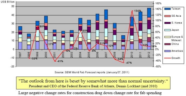
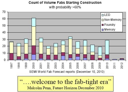
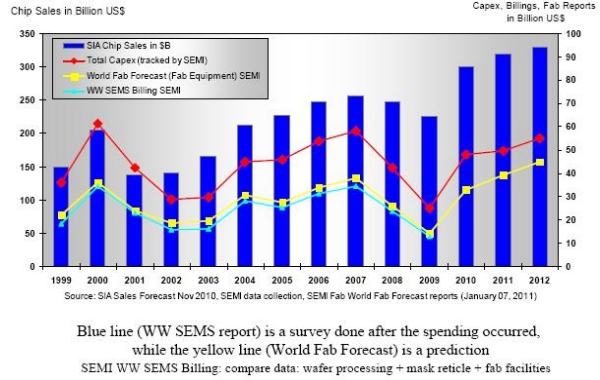
January 24, 2011 — Speaking at SEMI’s Industry Strategy Symposium (ISS) in January, Christian Dieseldorff, SEMI’s senior analyst, provided an in-depth look at fab construction, capacity, and capex in 2011 and 2012 (see figures).

Listen to Dieseldorff’s interview:  Download for iPhone/iPod users  or Play Now

In this podcast, Dieseldorff walks listeners through fab construction projects by region and device type (LED, non-memory, memory, etc.). He speaks with Debra Vogler, senior technical editor.

Click to Enlarge

Figure 1. Fab spending on front end facilities (Construction and equipping, including discretes). SOURCE: SEMI

Dieseldorff sees a decline in construction projects in 2011, followed by a double-digit decline in projects in 2012.

Click to Enlarge

Figure 2. Fab construction projects: Count of fabs vs. type. SOURCE: SEMI

Breaking out LED fabs, Dieseldorff notes that the largest growth regions (capacity and number of participating companies) are China, Taiwan and Korea. For 2011 and 2012, however, there aren’t many new LED fabs. 

Click to Enlarge

Figure 3. Equipping fabs — chip sales & capex trends: Both riding the same rollercoaster. SOURCE: SEMI

Subscribe to Solid State Technology/Advanced Packaging.

Follow Solid State Technology on Twitter.com via editors Pete Singer, twitter.com/PetesTweetsPW and Debra Vogler, twitter.com/dvogler_PV_semi.

Or join our Facebook group

(January 7, 2011 – RWE Australian Business News) — BluGlass (ASX:BLG) has commissioned the foundry services of  Rainbow Optoelectronics Materials Shanghai to provide device fabrication and processing services for the purposes of creating a nitride solar cell prototype designed by BluGlass.

The arrangement enables BluGlass to outsource the processing of its Indium Gallium Nitride (InGaN) solar cell designs to an expert group-III nitride company without the need to invest in additional capital equipment during the research phase.

BluGlass non executive director Alan Li is the general manager of Rainbow, a semiconductor device manufacturing company that provides nitride semiconductors (primarily LED displays) to more than 25 countries.

InGaN solar cells, if successful, promise to be long lasting, relatively inexpensive and the most efficient ever created. BluGlass is developing solar cell structure designs and now is now seeking to develop cell prototypes as part of its Climate Ready grant.

Copyright 2011 RWE Australian Business News Pty Ltd.All Rights Reserved

Subscribe to Photovoltaics World

Follow Photovoltaics World on Twitter.com via editors Pete Singer, twitter.com/PetesTweetsPW and Debra Vogler, twitter.com/dvogler_PV_semi.

Or join our Facebook group

April 27, 2010 – The Extreme Ultraviolet Lithography System Development Association (EUVA) says it has surpassed 100W output at intermediate focus for an EUV light source, another big step to address a big hurdle facing EUV lithography as a production-viable candidate for next-generation semiconductor manufacturing.

Led by members Gigaphoton and Komatsu (Gigaphoton was formed in 2000 by JV parents Komatsu and Ushio), the mark of 104W power output at 2.5% conversion efficiency utilized a 7.9kW CO2 laser radiated onto a 60μ-dia. Sn droplet target; magnetic fields were used for debris removal. To hike the power output to the ~180-200W expected to be required for full volume manufacturing will require further increasing the CO2 laser output and improving the conversion efficiency. The EUVA says this laser-produced plasma (LPP) source should scale to >200W in-band power at intermediate focus, using a 20kW CO2 laser.

In a statement, Gigaphoton president Yuji Watanabe said the company would start ramping operations this quarter in its facility toward initial volume production, with shipments of EUV light sources slated for sometime in 2011.

At this year’s SPIE, Cymer said its EUV source had topped 90W at raw output, though this was significantly reduced at the intermediate focus; its source roadmap, though, predicts 200W by 1H11 and 350-400W within two years.

The EUVA is also pursuing another EUV source alternative — work led by member XTREME in Germany has put together a discharge-produced plasma (DPP) source eyeing 115W at intermediate focus, with conversion efficiency of 3.5% (about 1.5× better than conventional values, the EUVA says).