Category Archives: Materials and Equipment

(March 8, 2010) STAMFORD, CT — Worldwide semiconductor capital equipment spending is projected to surpass $29.4 billion in 2010, a 76.1% increase from 2009 spending of $16.7 billion, according to Gartner Inc. Gartner cites a dramatic recovery in semiconductor orders for the equipment order surge.

"The dramatic semiconductor industry recovery rate over the last three quarters has necessitated a renewed growth for equipment spending," said Jim Walker, research vice president at Gartner. "Spending by the memory and foundry markets, along with the advancement to new technology nodes, will drive the semiconductor equipment segment in the first half of 2010. Quarterly growth will see a slight slowdown in the second half before capacity additions start ramping up the equipment industry again going into 2011."

In the midst of the recession, Gartner predicted a recovery of 45.3% in 2010. All segments of the semiconductor manufacturing equipment market declined in 2009, with an overall slide of about 42.6%, says Gartner. Following the significant declines in 2009, all segments of the semiconductor capital equipment market will experience extremely strong double-digit growth in 2010 (see Table 1).


Table 1. Worldwide semiconductor capital equipment spending forecast 2009-2014 (millions of dollars). Source: Gartner Inc, March 2010

Year:

2009 2010 2011 2012 2013 2014
Semiconductor capital spending 25,934.9 40,429.9 51,291.5 61,898.6 54,167.5 52,953.2
Growth (%) -41.1 55.9 26.9 20.7 -12.5 -2.2
Capital equipment 16,677.1 29,372.6 36,413.3 42,919.6 35,694.2 35,965.5
Growth (%) -45.6 76.1 24.0 17.9 -16.8 0.8
Wafer fab equipment  12,976.8 22,924.7 28,793.3 34,351.3 29,176.7 28,581.6
Growth (%)  -46.4 76.7 25.6 19.3 -15.1 -2.0
Packaging and assembly equipment  2,382.6 4,181.7 5,013.2 5,716.4 4,335.5 4,977.0
Growth (%) -40.4 75.5 19.9 14.0 -24.2 14.8
Automated test equipment  1,317.7 2,266.2 2,606.8 2,851.9 2,182.1 2,406.8
Growth (%)  -46.1 72.0 15.0 9.4 -23.5 10.3
Other spending 9,257.8 11,057.3 14,878.2 18,979.0 18,473.3 16,987.8
Growth (%) -30.8 19.4 34.6 27.6 -2.7 -8.0

Semiconductor fab

Overall worldwide wafer fab equipment (WFE) spending declined 46.4% in 2009, a slight improvement from the Q’04 2009 forecast. Worldwide WFE spending in 2010 will grow 76.6% from 2009. WFE spending will be driven by aggressive technology upgrades, especially for the leading memory companies. Utilization rates continue to run in the mid-80% to high 80% range for total utilization and in the low 90% for leading edge. Leading-edge utilization will hit the mid-90-percent range by the end of 2010, which will start to drive stronger capacity additions in 2011.

Packaging and test

After declining 40% in 2009, the worldwide packaging and assembly equipment (PAE) market is expected to increase by more than 75% in 2010, about 25 percentage points more than expected in last year’s forecasts. Decent PAE market growth is expected through 2012. The modest decline expected for 2013 is based on a more traditional inventory-based market contraction. On a regional basis, Asia/Pacific will improve its share of PAE consumption throughout the forecast period. From about 77% of PAE shipments in 2010, Asia/Pacific will account for nearly 85% of all PAE sales by 2014. China will be the largest individual consumer of PAE in 2012, accounting for nearly 27% of the total market that year.

2010 will bring the worldwide automated test equipment (ATE) market its first positive growth year since 2006. After bottoming out in the first quarter of 2009, the ATE market has realized substantial quarterly gains and is expected to grow by more than 70% in 2010. Growth is expected to continue during the next several quarters as device demand improves. Gartner’s 2010 growth expectations are driven heavily by the expected transition to DDR3 memory devices. On a regional basis; test equipment revenues will be driven by increased shipments to the Asia/Pacific region. By 2014, shipments to Asia/Pacific will grow to nearly 80% of the ATE market.

Post-recession semiconductor equipment sales growth

"The semiconductor equipment industry will experience a very strong growth spurt in 2010, as we emerge from a very costly recession, and this growth is expected to continue throughout 2012," said Mr. Walker. "However, we expect this upturn to be one of the first in which the peak revenue in capital equipment does not surpass previous growth cycles, which may well help to mitigate the boom/bust scenario that we have seen in the past."

Additional information is available in the Gartner report " Forecast: Strong Growth Propels Semiconductor Capital Equipment Market In 2010," http://www.gartner.com/resId=1313119. This research is produced by Gartner’s Semiconductor Manufacturing program, http://www.gartner.com/it/products/research/asset_129175_2395.jsp.

March 3, 2010 – Intel has given its nod to two dozen key partners from its roster of thousands of supply-chain contributors as the 2009 winners of its awards for Preferred Quality Supplier (PQS) and Supplier Continuous Quality Improvement (SCQI).

Click to Enlarge
(Image of statue from Intel.com)

To earn Intel’s top award, its "Supplier Continuous Quality Improvement" (SCQI) award — now in its 23rd year — 10 honorees (down from 16 in 2008) scored at least 95% on a list of performance and ability goals, including cost, quality, availability, delivery, technology, and responsiveness, over the past year. They also achieved ≥90% on an improvement plan and "demonstrated solid quality and business systems."

"These 10 suppliers were industry role models during the rapidly changing business environment of 2009," noted Brian Krzanich, SVP/GM of Intel’s manufacturing and supply chain, in a statement.

Another 16 suppliers (down from 26 in 2008) scored 80% or better to earn Intel’s 2009 "Preferred Quality Supplier" (PQS) recognition. All winners must also adhere to a "challenging" improvement plan and a quality/business systems assessment, and comply with the Electronic Industry Citizenship Coalition Code of Conduct and Intel’s own Environmental Social Governance program

One interesting tidbit from the listings: Intel now recognizes two lithography suppliers as PQS winners: incumbent litho tool supplier Nikon (which was a SCQI winner in 2008) and new recipient ASML. This, after an industry analyst recently suggested that ASML has won work in at least two layers with Intel’s 22nm work for now divided between the two platforms — shifting the balance of business within Intel to a 40%/60% split.

Intel launched the SCQI program in 1987 to improve the systems and output of key suppliers, in an effort to minimize the amount of time and money spent inspecting incoming material, goods, and services purchased. The company honored 40 companies in 2008, 48 suppliers in 2007, 54 suppliers in 2006, 38 in 2005, 43 in 2004, 45 companies in 2003, and 42 companies in 2002.

The 2009 SCQI winners are:

– * Daewon Semiconductor Packaging (injection molded trays)
– * DEK International (solder paste, flux printing machines)
– * Disco (precision cutting, grinding, polishing equipment)
– * Hitachi High-Technologies (etchers, FE-SEMs, CD-SEM, defect inspection tools)
– * Hitachi Kokusai Electric (diffusion furnaces)
– * Moses Lake Industries/TAMA Chemicals (ultrahigh-purity process and performance chemicals)
– * Munters (VOC abatement equipment)
– ** Senju Metal Industry (surface mount materials)
– * SUMCO (200mm and 300mm polished and test silicon wafers)
– ** Verizon Business (global communications)

Winners of the 2009 PQS award include:

– ** AceCo Precision Manufacturing (factory spares and refurbishment)
– Advanced Semiconductor Engineering (turnkey packaging and test services)
– ASML (lithography process tools)
– Cabot Microelectronics (CMP slurries)
– ** Cisco Systems (networking hardware infrastructure, IP telephony, enterprise collaboration)
– DAIFUKU (fab automated material handling systems)
– ** FUJIFILM Electronic Materials (chemistry, equipment for semiconductor device manufacturing)
– Grohmann Engineering (assembly capital equipment and engineering support)
– Hirata (material handling tools)
– * Nikon (lithography scanners)
– * Nippon Mining & Metals (sputtering targets for physical vapor deposition)
– Nordson ASYMTEK (dispense equipment)
– ** Praxair Electronics (electronic process and bulk gases, sputtering targets, spare parts management)
– ** Rofin-Baasel (laser mark equipment)
– ** Skanska (construction management)
– * Tokyo Electron (semiconductor production equipment)

(* a 2008 SQCI winner)
(** a 2008 PQS winner)


by Debra Vogler, senior technical editor, SST/AP

March 2, 2010 – Mentor Graphics Corp. unveiled its FloTHERM IC productivity tool targeting the semiconductor industry for thermal characterization and design at the recent SEMI-THERM Symposium (Santa Clara, CA USA). The new tool is a Web-based platform that automates the design tasks associated with full-spectrum thermal characterization and validation.

Ian Clark, product marketing manager at Mentor Graphics, told SST that the metrics in the tool are generated by the software automatically placing the package of interest in a virtual representation of the standard JEDEC test environments and performing a calculation using the tool’s solver. In one example (Figure 1), he noted that the metric of interest is the junction-to-moving air thermal resistance (Θjma). The tool output shows the surface temperatures of the test board and package in the free post-processing viewer, FloVIZ. "For this metric, the appropriate JEDEC test environment is the moving air (forced convection) configuration," explained Clark.

Figure 1. Surface temperature distribution on the test board and package for the moving air (forced convection) test environment as shown in the FloVIZ viewer.

In another example, Clark explained, the metric of interest is the junction-to-ambient thermal resistance (Θja). Figure 2 shows the surface temperatures of the test board and package and the flow field. "For this metric, the appropriate JEDEC test environment is the still air (natural convection) configuration," said Clark.

Figure 2. Surface temperature distribution on the test board and package and the flow field for the still air (natural convection) test environment as shown in the FloVIZ viewer.

According to the company, a typical semiconductor thermal team spends ~60% of its time on standard package thermal characterization and design, and the remaining time for customer-specific characterizations. The FloTHERM IC tool dramatically reduces the time spent on thermal characterization and design by providing an automated process that includes pre-verified thermal models to reduce the risk of modelling errors. Clark also noted that the tool can achieve reductions of up to 25% in the time usually needed for customer-specific characterizations.

The FloTHERM IC tool is based on Mentor Graphics technologies including FloTHERM computational fluid dynamics (CFD) software, used to simulate airflow, temperature and heat transfer in electronic systems, and the FloTHERM PACK Smart Parts modeling tool.

by Neha K. Choksi, independent consultant

March 2, 2010 – It has been more than a decade since Kris Pister introduced the concept of "smart dust": a distributed wireless network of sensors with self-contained sensing, computation, communication, and power. Although there are a handful of companies in this space (Crossbow Technology, Dust Networks, GainSpan, Arch Rock, for example), distributed wireless sensing networks have yet to hit main stream. At the IEEE Bay Area Nanotechnology meeting on February 16, 2010, Dr. Peter Hartwell revealed new efforts at Hewlett Packard that could change all of that.Click to Enlarge

Hartwell predicts that sensors will impact human interaction just as the Internet revolution did in the last decade. The impact is just beginning — free-fall and shock detection to park the hard drive, Wii motion sensors, image stabilization on mobile devices, and tilt monitors in washing machines, to name a few. HP’s Central Nervous System for the Earth (CeNSE) is leveraging multiple HP business units to achieve distributed sensing networks. This takes sensing to the next level by allowing a system to incorporate surrounding information to make its own decisions. Hartwell refers to this next phase as "aware computing." The opportunities for this technology are limitless: food safety, disaster prevention, and resource management, to name just a few.

For example, home intrusion systems could sense and distinguish the difference between a human intruder or the movement of a family pet and make smarter alarm trigger decisions. During a Powerpoint presentation, a system can detect noise (speaking) and bypass the screensaver mode that often appears while a speaker is at the podium. With "aware computing" auto shut-off light systems in offices and conference rooms will not need to rely on macro movement for sensor activation. Sensors would be able to detect breathing, noise, and smaller vibrations to determine somebody’s presence to keep the lights on. Hartwell refers to these opportunities as "low-hanging fruit" to increase energy efficiency.

HP’s CeNSE nodes will include vibration, tilt, navigation, rotation, and sound sensing by leveraging their new revolutionary 6 axis motion sensor. This new accelerometer design has significant advancements — but HP’s solution goes well beyond their novel accelerometer design. In addition to detecting motion, HP is working on chemical and biological sensors by surface-enhanced Raman spectroscopy (SERS) and nanostructures to create miniaturized chemical analysis sensors. By coating nanostructured silicon with silver, HP is able to enhance the signature photon reflection used to identify a sample. This gain factor enables system miniaturization and smaller sample sizes to achieve broad chemical analysis.

One factor limiting the speed of adoption for distributed sensing networks is the cost. Currently available sensor nodes on the market cost in the range of $300-$400 per node. Depending on the application, one million nodes may be necessary, making the current node cost-prohibitive for a fully distributed network. HP’s technology will leverage the large-volume manufacturing know-how at their inkjet fabrication site in Corvalis, OR, and technology advancements in the sensor device to build a small low-cost sensor node that is orders-of-magnitude more cost-effective than nodes currently available. As Hartwell puts it, high performance, small, and low cost are the "magic button" and "holly grail" of distributed sensing networks. By making the nodes themselves essentially free, the value will be based on computing the data obtained from these sensors and using this insight to provide useful information to customers.

HP plans are not limited to just the sensor nodes themselves. With the large data that would become available with million node systems, HP must address how to deal with the data. Hartwell envisions the data processing within the network. HP plans to address this by leveraging their memristor technology. This could lead to a fundamental change in computing architecture. Memristors display a non-linear switching characteristic, enabling a teachable platform for data computing.

HP is leveraging multiple units within the company for the CeNSE project. The company’s acquisition of EDS provides the communications infrastructure and business process outsourcing needed to make the picture complete. HP’s CeNSE initiative aims to provide the total solution to distributed networks: sensor nodes, data computing, and the communications infrastructure. Hartwell asserts that HP will lead the technology revolution with their one-stop shop into what he refers to as "the next wave of the future."

But for HP, this wave is no longer limited to the future. HP has announced its partnership with Shell to acquire extremely high-resolution seismic data on land for more efficient methods of finding and producing petroleum — and reduce the impact on the environment in the process.

Despite all of the potential applications, one can’t help but ask what new dilemmas distributed sensing might pose. "In parallel with the implementation of such a network, would it not be apropos to work on policies that ensure that these networks are used for the common good?" asks John Berg, CTO of American Semiconductor Inc. Nevertheless, the opportunities are abound and HP plans to be poised and ready with a total solution for the eruption of distributed network sensing.


Neha K. Choksi is an independent consultant for companies including SmallTech Consulting LLC, 325 Sharon Park Drive #632, Menlo Park, CA 94025, www.SmallTechConsulting.com, e-mail choksi [at] gmail.

by Thorsten Matthias, Markus Wimplinger, Paul Lindner, Bioh Kim, Eric Pabo, Dustin Warren, EV Group

Executive overview
The advantages as well as the technical feasibility of through-silicon vias (TSV) have been acknowledged by the industry. Today, the major focus is on the manufacturability and on the integration of all the different building blocks for TSVs and 3D interconnects. In this paper, the advances in the field of lithography, thin wafer processing and wafer bonding, are presented, with an emphasis on the integration of all these process steps.

Copyright © 2009 by International Microelectronics And Packaging Society (IMAPS). Permission to reprint/republish granted from the 42nd International Symposium on Microelectronics (IMAPS 2009) Proceedings, pg. 563-568, November 1-5, 2009, San Jose McEnery Convention Center, San Jose, California. ISBN 0-930815-89-0.

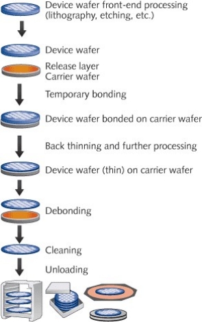
March 1, 2010 – Face-to-back integration schemes require the processing of thin wafers for both wafer-to-wafer and chip-to-wafer stacking. Prior to thinning, the device wafer is mounted on a carrier wafer with a temporary wafer bonding step. 300mm wafers with a thickness of 30μm have been successfully processed through the complete TSV process line.

Lithography on the backside of the thin device wafer requires alignment of the photo-mask to the alignment keys buried in the bond interface. After backside processing, the thin wafer is debonded from the carrier wafer. The thin wafer is either mounted on dicing tape for singulation and subsequent chip-to-wafer stacking, or it is bonded immediately to another device wafer for wafer-to-wafer stacking.
Click to Enlarge
Figure 1. Process flow of thin wafer processing by temporary bonding and debonding.

For applications with very high TSV density, face-to-face integration schemes using Cu-Cu thermo-compression wafer bonding are a promising approach as the electrical contacts are established in parallel to the mechanical bond. Alternatively, fusion bonding is very attractive due to the cost-of-ownership advantages compared to metal-metal bonding. Recent equipment and process improvements enable sub-micron alignment accuracy on 300mm wafers.

3D integration and TSVs

Extensive research and development activities over many years have shown the feasibility as well as the technical advantages of through-silicon vias (TSV) and 3D integration. Many different manufacturing and integration schemes are being discussed and evaluated. Most or all of the individual process steps and building blocks have been successfully qualified. Today, industrial consortia such as EMC-3D focus on cost competitive manufacturability and on the integration of all the different building blocks for TSVs and 3D interconnects.

Vertical or 3D stacking of chips can be realized as chip-to-chip (C2C), chip-to-wafer (C2W) and wafer-to-wafer (W2W) manufacturing. The stacking of the chips itself can be realized as face-to-face or face-to-back integration [1]. Face-to-back integration requires wafer thinning and processing of the device wafer on the front- and backsides prior to permanent bonding of the dies or wafers.

Thin wafer processing

The ongoing demand for smaller and smaller devices requires minimizing the diameter of the TSVs. Although TSVs can be manufactured with quite extreme aspect ratios, the manufacturing costs are significantly lower for moderate or low aspect ratios of 1:5 up to 1:10. Therefore, small via diameters require thin device wafers.

Figure 1 shows the generic process flow for thin wafer processing with temporary bonding to a carrier wafer. The starting point is a device wafer with complete front-end processing on the frontside of the wafer. This device wafer is bonded to a carrier wafer with its frontside in the bond interface. After bonding the first step is back-thinning of the wafer. Usually, back-thinning is a multistep process consisting of mechanical back-grinding and subsequent stress relief etching and polishing. After back-thinning, the backside of the device wafer can be processed using standard wafer fab equipment. The carrier wafer gives mechanical support and stability and protects the fragile wafer edge of the thin wafer. Finally, when all backside processing is done, the wafer gets debonded, cleaned, and transferred to a film frame or to other output formats. Temporary bonding and debonding are enabling technologies for wafer-level processing of thin wafers. The main advantages of temporary bonding and debonding using a carrier wafer are compatibility with a number of processes and equipment, for example:

Standard fab equipment. The bonded wafer stacks literally mimic a standard wafer. The geometry of the bonded stack can be tailored in such a way that the resulting geometry is in accordance with SEMI. This brings the advantage that standard wafer processing equipment can be used without any modification. There is no need for special end-effectors, wafer chucks, cassettes, or pre-aligners. No downtime at all is required to switch between processing of standard thick wafers and temporarily bonded thin wafers.

Existing process lines. With the addition of only two pieces of equipment, the temporary bonder and the debonder, a complete process line or even fab becomes able to process thin wafers.

Existing processes. The mechanical and thermal properties of the bonded wafer stack are very similar to a standard thick wafer. This enables the use of existing wafer processing recipes, which have been proven and qualified for standard wafers.

Future process flows. The user has the full flexibility to change the processing sequence and the individual process steps for backside processing. After temporary bonding, the device wafer is securely protected against mechanical damage. Furthermore, adding process steps or modifying the process flow does not impact the cost of ownership for thin-wafer processing.

Product roadmaps. For many devices and products, the roadmaps lead to even thinner wafers in the future. With temporary bonding, the entire backside processing becomes independent of the wafer thickness. Reducing the wafer thickness does not require any modifications or adjustments to the processing equipment.

An important point is the choice of the carrier wafer. For silicon-based devices, the recommended carrier is a standard silicon wafer. First of all, with a silicon carrier, the resulting bonded stack mimics very closely a standard wafer. From a geometrical point of view, this enables the use of standard wafer processing equipment without modifications, whereas oversized carriers would require special wafer chucks and cassettes for the wafer stack.

Even more important are the thermal properties of the bonded stack. With a silicon carrier, the thermal expansion between device wafer and carrier is perfectly matched. Using a non-silicon carrier would cause the stack to bow and warp due to thermal expansion mismatch. There is the risk that the induced stress impacts the processing characteristics and ultimately the device performance. CTE-matched glass carriers create a different problem — metal ion contamination. It is not possible to use these glass carriers in CMOS fabs, which undermine one of the major advantages of the carrier wafer approach — the ability to process frontside and backside of the device wafer on the same equipment set.

Lithography for temporarily bonded wafers

For many integration schemes, after thinning and polishing, the backside of the thin device wafer has to be patterned with one or more mask levels. Due to the similarity between a bonded stack and a single wafer, standard spin coating and developing processes can be applied. Features such as bond pads, pillars, and bumps are typically created on a mask aligner. The exposure of the resist coated surface requires the alignment of the mask to the features on the device wafer front side, which is buried in the bond interface. Modern mask aligners have integrated IR alignment capability for this application (Figure 2).

Click to Enlarge
Figure 2. Front-to-backside lithography for a thin device wafer bonded to a carrier wafer. The alignment keys on the device wafer front side are buried in the bond interface. The alignment to the mask is performed with infrared (IR) alignment.


Permanent wafer bonding

There are three main wafer bonding methods for 3D interconnects: fusion (or molecular) bonding, adhesion thermo-compression bonding, and metal-metal thermo-compression bonding. In addition, there are hybrid methods such as simultaneous adhesive-metal bonding or simultaneous fusion-metal bonding. Each of these methods has advantages and disadvantages. Adhesion wafer bonding is not sensitive at all to particles; metal-metal thermo-compression bonding simplifies the process flow as the mechanical and electrical connections are established simultaneously in one process step [1].

Fusion wafer bonding is a two-step process consisting of room temperature pre-bonding and annealing at elevated temperature. The classical annealing schemes, which were developed for SOI wafer manufacturing, require annealing temperatures in the range of 800-1100°C. A surface pre-processing step, LowTemp plasma activation, enables the modification of the wafer surface in such a way that the annealing temperatures can be reduced to 200-400°C. Therefore, this type of plasma activation enables the use of fusion wafer bonding for 3D integration.

Fusion wafer bonding brings several advantages:

Alignment accuracy. By bonding at room temperature, bonding misalignment based on thermal expansion of the wafers is eliminated completely. Figure 3 shows alignment results with the EVG SmartView NT Aligner.

Click to Enlarge
Figure 3. Alignment results with the EVG SmartView NT Aligner: 400 alignments

Due to the very good alignment accuracy, fusion wafer bonding is especially well suited for high density TSV devices. The ITRS roadmap for high density TSVs specifies via diameters of 0.8-1.5μm in 2012 [2]. Sub-micron post bond alignment accuracy is necessary for these devices.

Throughput. Fusion wafer bonding has the highest throughput compared to adhesive or metal-metal thermo-compression bonding because it is a room temperature process. It can be implemented either as an in situ bond process in the aligner module or as an ex situ process under vacuum in a bond module. The subsequent annealing can be performed as a batch process in a furnace or oven.

Inspection capability after pre-bonding prior to final annealing. After the room temperature pre-bonding step, the bond strength is sufficiently high to enable inspection of bond quality and alignment accuracy. In case of misalignment or bond quality problems, e.g., voids, the wafer pair can be separated and reworked. This concept of inspection and, if necessary, reworking prior to final annealing has been used in SOI wafer manufacturing for many years.

Cost-of-ownership. The combined effects of in situ bonding in the aligner module, highest throughput, increased yield due to the ability to rework and reduced capital costs results in low cost-of-ownership for manufacturing schemes based on fusion wafer bonding.

The primary challenges for fusion wafer bonding are the sensitivity to particles and the specifications for surface roughness. Any particle within the bond interface will create an un-bonded area, a void. The size of the void can be up to 1000 times larger than the particle itself. A void in the bond interface will not only damage the directly impacted dies, but it may even prevent back thinning and thereby cause loss of the entire wafer. To overcome this threat, modern wafer bonding systems include wafer cleaning modules within the bonding platform. This equipment configuration enables cleaning of the wafer surface immediately prior to wafer bonding. Because of the integrated cleaning modules and the ability to rework the bonded wafers, the sensitivity to particles is no longer perceived as an issue for high-volume manufacturing.

Fusion wafer bonding requires surface micro-roughness in the range of 0.5-1nm. These requirements can be met with modern CMP technology.

Bond alignment inspection

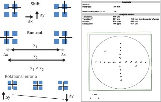
Post-bond alignment inspection is a critical process control step. A misaligned wafer bond can result in total loss of two fully processed wafers. Therefore, it is important to analyze all the contributing factors to the alignment accuracy. Figure 4 shows the different factors contributing to misalignment, as well as the process control output format for a bond alignment inspection system.
Click to Enlarge
Figure 4. Left side: Potential alignment errors: shift, rotational misalignment and run-out; the post-bond alignment is often an overlay of all three types. Right side: The post bond alignment inspection system EVG40 NT allows customer defined wafer mapping.

Conclusion

In this paper, significant improvements in manufacturing processes and equipments have been presented. Thin wafer processing is becoming a mainstream process. Temporary bonding to a carrier wafer, thinning, backside processing and subsequent debonding have been qualified for several different process flows. Using a silicon wafer enables the use of standard fab equipment for thin wafer backside processing. The SmartView NT aligner allows alignment accuracy in deep sub-micron range. Fusion wafer bonding has some unique advantages for 3D integration namely alignment accuracy and throughput. Process control including post bond alignment inspection is critical for improved yield and cost-of-ownership.

Acknowledgments

LowTemp and SmartView are registered trademarks of EV Group.

References
[1]. P. Garrou, C. Bowers, P. Ramm (Eds.), "Handbook of 3D integration," Wiley, 2008.
[2]. www.itrs.net

Biography

Thorsten Matthias is director of business development at EV Group, Erich Thallner Strasse 1, 4782 St. Florian/Inn, Austria, e-mail: [email protected].

February 23, 2010 – Demand for semiconductor manufacturing equipment continues to surge as the industry emerges from its slumber, with some measurements showing strength not seen in several years, according to the latest monthly data from SEMI.

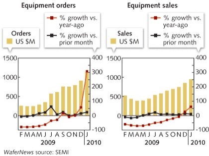
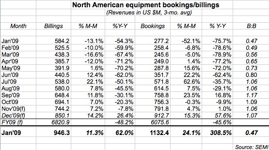
Figures from North America-based tool suppliers indicate worldwide bookings (orders) rose to $1.13B in January 2010, their highest in nearly two years — that’s up 24% from December levels and more than 3× higher than January 2009, near the bottom of the slump. Billings (sales) also performed well in January, up 11% from December and 62% higher than a year ago. Even December’s numbers were better than initially thought, especially in bookings which were revised up about 6% (an extra $50M).

Click to Enlarge

Perhaps the best number of the bunch: the book-to-bill ratio (B:B), a measuring stick for business coming in (orders) vs. going out (sales), soared to 1.20 in January, its highest level in more than six years and a reflection of "the robust capex spending plans announced by semiconductor device manufacturers over the past several months," noted SEMI president Stanley Myers, in a statement.

Click to Enlarge

This B:B trend bears watching, as talk about the industry recovery turns from "when" to "how long will it last." The B:B finally cracked the 1.0 parity mark in late summer, so a string of above-parity marks indicates good business ahead. There is still some question, though, whether the industry is in the midst of a strong 1H10 investment climate, only to fall off to another slowdown in 2H10 — or whether factors such as increased tool lead-times (e.g. lithography equipment) will extend the streak into 2011.

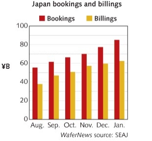
Numbers from Japan’s semiconductor equipment sector also continue to be strong, according to the Semiconductor Equipment Association of Japan (SEAJ). January’s orders came in at roughly ¥85B (US $931M), up 10% from December and 237% from a year ago, while sales rose about 5% month-on-month and 36% year-on-year to ¥62.5B ($683M). The B:B remains well above parity at 1.36; it has only dipped below 1.30 once in the past six months.

Click to Enlarge

(February 16, 2010) — The VectorGuard stencil portfolio from DEK now includes the double layer Platinum stencil, a stencil technology that is said to offer performance benefits over conventional screens. VectorGuard Double Layer Platinum stencils suit semiconductor applications and component manufacture, solar cell manufacture, low-temperature co-fired ceramic (LTCC) manufacture, as well as other production challenges requiring fine line or mixed feature sizes.

The double-layer stencil is fabricated through a two-step lithography and nickel electroforming process then mounted on VectorGuard tensioning technology. The mesh layer of the two-layer structure serves to hold the stencil intact while accurately controlling the flow of paste to the second layer. The circuit layer determines the thickness and shape of the print deposits to deliver high tolerance, fine-dimension printing. The stencils can print long conductive lines without losing strength.

The product is said to generate a tenfold increase in product lifetime over screens.  It reduces the two-step process for multi-layer technologies such as LTCC to one by combining filling and inner-layer printing stages. It is also reportedly easier to clean and maintain than a screen. Dimensional accuracy reaches better than 0.1 µm/mm. The new DEK stencil also incorporates all the operational advantages of the reusable, recyclable VectorGuard system, including ease-of-use, system rigidity and operator safety.

For more information on DEK, visit www.dek.com.

by Robin Bornoff, Mentor Graphics Corp.

This case study, a partner piece to Robin Bornoff/Mentor Graphics’ discussion of fluid dynamics analysis for IC package design, examines how IDT used CFD thermal analysis in a packaging decision for a recent product launch.

February 16, 2010 – Integrated Device Technology Inc. (IDT, San Jose, CA) develops mixed signal semiconductor solutions for digital media and other applications. The company’s power-smart solutions optimize system level performance while maximizing device performance. Controlling semiconductor junction temperature for optimal system performance and lower cost is critical, since IDT products are commonly used in compact platforms such as LCD televisions.

IDT used thermal simulation and analysis in preparation for a recent product launch. This device was a multichip module containing two separate silicon elements — a processor and a clock. The thermal requirements stated that the temperature difference between the two chips was not to exceed 0.1°C. Temperature affects the frequency of both chips, so both must operate at effectively the same temperature.

Two die placement alternatives were in the running: side-by-side on a die paddle, or stacked. Differences in the die-attach material cause the two configurations to differ in thermal resistance. Side-by-side offers lower thermal resistance between the two dice (and lower assembly costs) but requires more board real-estate. Stacked die take up less space but typically have slightly higher thermal resistance and assembly costs. Jitesh Shah, advanced packaging engineer at IDT, created thermal models to compare the two configurations. He looked at a half-dozen design alternatives over ambient conditions ranging from -55°C to 85°C.

Using Mentor Graphics FloTHERM to simulate the alternatives, Shah discovered that the stacked die delivered better performance. "I had assumed that a side-by-side arrangement would provide the best thermal performance since the die-attach materials in that configuration were 3× more conductive than the stacked-die option," Shah said. "But looking more closely at the simulation results, I determined that even with lower conductivity thermal interface material, the stacked-die approach outweighed the expected benefits of the side-by-side approach."

Because the IC is intended for hand-held consumer products with very limited board real-estate, the more space-efficient stacked-die approach provides a significant advantage to end-product manufacturers. In this case, thermal simulation reduced product development expenses by reducing the need for physical testing and late-stage design changes.

Acknowledgment

FloTHERM is a registered trademark of Mentor Graphics Corp.

Biography

Robin Bornoff received a mechanical engineering degree from Brunel U. (UK) in 1992 followed by a PhD in 1995 for CFD research. He is FloTHERM and FloVENT product marketing manager at Mentor Graphics Corp., Mechanical Analysis Division, 81 Bridge Road Hampton Court Surrey KT8 9HH, UK; ph.: +44 (0)20 8487 3084; e-mail [email protected].

by Robin Bornoff, Mentor Graphics Corp.

February 16, 2010 – Most people imagine integrated circuit designers spending their days laying out unimaginably small, complex features on silicon. But the IC design process spans many disciplines, including the job of packaging those powerful but delicate silicon chips. IC packages must deliver signals to and from the chip inside, but equally important, they must carry potentially destructive heat away from the active component.

Package thermal design and evaluation are both labor- and time-intensive tasks when done the traditional way. This involves special standardized fixturing, a "thermal die," a host of measurement tools, and up to six weeks of preparation and testing.

But some form of testing is indispensable. Ever-improving processes and tools allow IC designers to pack more functionality into smaller chips with each passing year. One by-product of these steady improvements is the greater concentration of heat within devices that execute millions of operations per second, every second. IC design teams must find ways to minimize heat generation and buildup, and thermal testing is part of the process.

Producers have learned to expect up to 20% of initial thermal designs to fall short of specified targets and fail their first evaluation, requiring additional test iterations. Product planners usually build a cushion into their development timelines, but even liberal padding won’t salvage a schedule that suffers the delays that result from too many cycles of redesign and evaluation.

Small wonder, then, that IC manufacturers are constantly exploring better solutions to the costly problem of package evaluation and testing.

A methodology in transition

Traditionally, package design engineers have followed a complex but universally-accepted physical test regime that evaluates the thermal performance of new packaging configurations within a standard environment defined by the JEDEC Solid State Technology Association.

The tests are performed by mounting the packaged part on a JEDEC-standard board and testing the assembly in natural-convection and forced-convection environments. A thermal die equipped with integrated forward-biased diodes measures the junction temperature inside the packaged part. The cycle time for collecting each set of data ranges from 4 to 6 weeks. This long time span encompasses the re-design and assembly of the package, plus the actual testing steps.

While the results usually correlate well with the device’s behavior in the real world, physical testing has a glaring weakness: it isn’t possible to evaluate the thermal performance of a new product or package until the first prototypes arrive. This occurs relatively late in the design process, when setbacks are least affordable. Fortunately, most (80% to 90%) of new designs pass satisfactorily. But first-round failures face a schedule delay of up to six weeks.

Business calculations anticipate a certain proportion of failures. Once a device has failed, there is a crash effort to modify and re-test the design. Obviously this process, with its multi-week delays, is not one that can be repeated again and again while engineers fine-tune the design. After a device has used up its allotment of risk, developers must rely on proven, high-confidence measures to correct any remaining problems. It is not an atmosphere conducive to experimentation or innovation. There simply isn’t enough time to try alternative approaches and optimize thermal performance.

But the intense pressures in today’s product-development environment have fostered a demand for both short cycles and low risk. No longer is it practical to rush package designs to completion in the expectation that "most" will meet their thermal goals. Increasingly, IC and package designers are turning to thermal modeling tools to perform complex tests in the virtual realm and deliver predictions without prototypes — at least not in their tangible hardware form. Proposed designs can be validated early and often, minimizing the risk of prototype test failure.

Thermal modeling and virtual packages

Modern thermal modeling solutions are based on a discipline known as computational fluid dynamics (CFD). It is a field well known and appreciated among mechanical designers who must consider fluid flows — whether the fluid is water, atomized fuel, or heated air — in their designs. Forecasting fluid behaviors for even the simplest systems with ordinary manual calculations is almost impossibly complex. CFD comes to the rescue by accepting inputs about a particular flow environment and processing millions of numerical equations to develop a composite result that accurately predicts fluid flow.

Until recently, CFD was the province of trained specialists who could design optimized calculating grids called meshes, define cavities and boundaries, and generally minister to a set of rarified input requirements. Today, that situation is changing and CFD solutions for flow applications including high-temperature thermal analysis are within the reach of engineering and IC package design departments throughout the industry. (IDT, for example, recently used CFD thermal analysis in a packaging decision for a recent product launch.)

Late-breaking CFD advancements are emerging to further assist IC package designers. Web-based solutions are now available to generate thermal models of IC components, test boards, and associated elements. These sophisticated generators produce reliable and accurate "virtual" packages in just a fraction of the time required when using traditional methods. The models are tailor-made for CFD analysis.

Today, two formerly daunting and time-consuming tasks — first, model creation and then CFD analysis — can be handled efficiently by accessible software-based tools. The packaging engineer is liberated from the constraints of physical testing and can freely experiment with new ideas and design variants without risking an entire project’s success.

A tour of a simulation procedure

An accurate CFD analysis relies on the accuracy of the model from which it works. An engineer begins his or her thermal evaluation not by running a CFD application, but by entering IC package parameters into the web-based model development tool. These characteristics include package type and size, lead or ball count, substrate cross-section, die size, and more. The model generator sits atop a database that supports a host of package types and variants. It can produce any of three different model types:

The detailed model. This model describes package features in full. This method’s thermal performance calculations are the most accurate of all the approaches but the process requires significantly more computing resources than the other alternatives.

The two-resistor compact model. This model is generated using a computational implementation of the JEDEC standards for the Junction-to-Case and Junction-to-Board resistances. The burden on computing resources is very small but the worst-case error in junction temperature predictions can approach 30% and vary greatly between differing package types.

The DELPHI compact model. This is a significant improvement over two-resistor models. In many applications, the model will predict the junction temperature to an accuracy of 10% while greatly reducing simulation time. DELPHI compact modeling standards are currently being adopted by JEDEC.

The thermal resistor method of component representation discloses no proprietary intellectual property regarding the design or construction of the package. Therefore, the model can be freely delivered to system integrators, who can further verify that the thermal performance of the package within their actual product is compliant.

Once a thermal model of the package is generated, the CFD analysis can proceed. The model supplants the hardware prototypes of the past, yet supports the same level of rigor in the testing process. And crucially, it is easy to modify, test again, modify again, and so on.

To run the thermal analysis the engineer must define a JEDEC standard environment for the CFD-based thermal simulation tool, and then insert the package model into that domain. The simulation results provide a complete understanding of the thermal performance of the design. They include not only the temperature difference between ambient and the junction, but also the temperature of every point within the "system."

The simulation quickly points out any regions that exhibit high thermal resistance. These are obvious areas for improvement in thermal performance. Heat spreaders, slugs, and increased copper plane thickness are among the solutions that can remove heat from the silicon and reduce temperatures.

Figure 1. Thermal simulation of a plastic BGA device using 1oz copper planes in the package substrate to dissipate heat. With temperatures approaching the maximum in some areas, the device is not suitable for its intended application.


Figure 1
depicts the results from a simulation on a mixed-signal device housed in a plastic ball grid array (BGA), while Figure 2 provides a close-up view of the immediate die area. As the scale reveals, the temperature in that critical area is in the 124°C range — too hot for the health of the chip. The virtual device used in the simulation incorporates conventional 1oz copper planes to manage the heat transfer and these are not doing an adequate job.

Figure 2. Close-up view of the BGA showing the 124°C heat buildup in the center of the die area.

Thus, the simulation has provided insights that can help the designer improve the performance of the product. A more robust heat transfer medium is needed, and the modeling toolset offers slugs and other heat spreaders. It is important to note that this whole process can occur very early in the development cycle since software constructs are much easier to "prototype" than are hardware packages. Designers can evaluate many different designs and optimize the thermal performance in the time it would take to test just one or two variants with hardware-based analysis.

Pursuing this line of thinking, one might add a slug to the device and boost the thickness of the copper planes to 2 oz. Indeed, this does improve the heat situation, as shown in the simulation in Figure 3a. The scale reveals that the maximum temperature is now 115°C, well within the planned limits. However, both measures add cost to the device. Will just one of the two treatments suffice?

Figure 3. a) A simulation of the BGA with 2 oz. copper planes and a heat slug added. The temperatures are now well under maximum levels, though at added cost; b) results after removing the slug. The temperatures have been held to an acceptable level (119°C) while maintaining costs close to those of the more basic package scheme described in Fig. 1.

The simulation in Fig. 3b proves that it will. The slug can be eliminated at the cost of just a few more degrees of heat buildup. The final peak temperature, 119°C, is still safely within limits. Both of these simulations can be completed in hours instead of the days required for hardware-based testing. All of the simulations shown in this example were developed with the Mentor Graphics FloTHERM analysis package using models generated on the FloTHERM PACK web-based toolset.

Conclusion

Until now, hardware tests have been the standard operating procedure for conducting thermal analysis. But these procedures are time-consuming and today’s market pressures demand results much faster than ever before.

Package designers are increasingly turning to software-based device modeling and CFD analysis solutions. These tools bypass hardware prototypes and allow timely evaluation of new concepts, eliminating time-consuming fabrication of trial components, thermal dice, and other fixturing. Now, it is possible to preview the impact of design decisions and changes without risking project success.

Acknowledgment

FloTHERM is a registered trademark of Mentor Graphics Corp.

Biography

Robin Bornoff received a mechanical engineering degree from Brunel U. (UK) in 1992 followed by a PhD in 1995 for CFD research. He is FloTHERM and FloVENT product marketing manager at Mentor Graphics Corp., Mechanical Analysis Division, 81 Bridge Road Hampton Court Surrey KT8 9HH, UK; ph.: +44 (0)20 8487 3084; e-mail [email protected].

February 3, 2010 – Researchers at Rice U. have figured out a way to transfer patterns of carbon nanotubes from a substrate to any other surface in a single dry room-temperature step, and then reuse the substrate with intact catalyst particles to grow more.

The research, published in ACS Nano, started with first-year postgrad Cary Pint "playing around with water vapor" to clean up amorphous carbons on some single-walled carbon nanotubes (SWNT), and discovering that the nanotubes he was extracting stuck to the tweezers — this led to investigating how the process could transfer CNTs to other surfaces. In his work, CNTs are grown via chemical vapor deposition (CVD) and etched with a mix of hydrogen gas and water vapor to weaken the bonds formed with the metal catalyst. Once stamped, the CNTs lay down and adhere via van der Waals forces to the new surface, leaving all traces of the catalyst behind.


A potassium bromide window covered by a film of single-walled carbon nanotubes, transferred from the growth substrate, which serves as a template, at right. (Source: Rice U.)


Among the results of the work: a crisscross film of nanotubes made by stamping one set of lines onto a surface and then reusing the catalyst to grow more tubes and stamping them again over the first pattern at a 90-degree angle. The process took about 15 minutes.

Eventually Pint sees the technique, which he says can scaled up "easily," can be used to embed nanotube circuitry into electronic devices. Future steps for the process are to make highly efficient optical sensing devices, and look at doping techniques to enable more precise growth of metallic (conducting) or semiconducting SWNTs.

His own goal is to develop the process to make a range of highly efficient optical-sensing devices. He’s also investigating doping techniques that will take the guesswork out of growing metallic (conducting) or semiconducting SWNTs.

The paper also describes a process for quickly and easily termining the range of diameters in a batch of nanotubes grown through chemical vapor deposition, something many spectroscopic techniques can’t do for structures >2nm in diameter. "This is important since all of the properties of the nanotubes — electrical, thermal and mechanical — change with diameter," Pint said. The good news: the method involves a Fourier transform infrared (FTIR) spectrometer, which "nearly every university has …sitting around that can do these measurements," he added.

From the ACS Nano paper abstract:

Utilizing this transfer approach, anisotropic optical properties of the SWNT films are probed via polarized absorption, Raman, and photoluminescence spectroscopies. Using a simple model to describe optical transitions in the large SWNT species present in the aligned samples, polarized absorption data are demonstrated as an effective tool for accurate assignment of the diameter distribution from broad absorption features located in the infrared. This can be performed on either well-aligned samples or unaligned doped samples, allowing simple and rapid feedback of the SWNT diameter distribution that can be challenging and time-consuming to obtain in other optical methods. Furthermore, we discuss challenges in accurately characterizing alignment in structures of long versus short carbon nanotubes through optical techniques, where SWNT length makes a difference in the information obtained in such measurements. This work provides new insight to the efficient transfer and optical properties of an emerging class of long, large diameter SWNT species typically produced in the CVD process.