Category Archives: Materials and Equipment

October 7, 2009 – IQE plc has agreed to acquire UK compatriot NanoGaN, which offers processes and IP related to gallium nitride (GaN) materials and devices, for approximately £0.4M, but could increase to £3.6M pending performance goals.

The deal widens IQE’s portfolio into high-growth markets such as laser projection, optical storage (e.g., BlueRay), laser printing, and solid-state lighting — high-brightness LEDs and solid-state lighting, for instance, use GaN substrate-based blue and green semiconductor lasers. NanoGaN’s technology also will bolster IQE’s footprint in high-power RF applications.

IQE — already an epitaxial materials supplier to NanoGaN, a Bath University-spinoff — says it will help complete development of commercial products and transfer NanoGaN’s Nanocolumn technology to its own high-volume production facilities, with sales expected to start in 2010. IQE has six manufacturing facilities spanning the UK, US, and Singapore.

"The acquisition of NanoGaN represents a major milestone in our technology roadmap, and reinforces our strategy of being a powerful IP based technology leader in the supply of advanced semiconductor materials to a multitude of high growth markets," said Drew Nelson, IQE CEO, in a statement, adding that NanoGaN "provides a perfect complement to our existing wireless and opto, and emerging solar businesses."

NanoGaN CEO Wang Nang Wan, newly appointed chief scientific advisor to IQE, noted that the deal "represents a unique opportunity for the commercializing of NanoGaN’s world leading technology and cements our long term relationship with IQE."

by Debra Vogler, senior technical editor, Solid State Technology/Advanced Packaging

September 28, 2009 – Earlier this month, Süss MicroTec launched its PA300PS 3D probe station targeting 300mm electrical probing of 3D stacked structures at the wafer-level. (The company already has wafer bonders and lithography equipment for 3D integration.) Among the probe’s features are an alignment function for vertical probe card technologies (MicroAlign), with an automated thermal management (ATM) system for active thermal compensation at various test temperatures. The mechanical stability of the chuck system enables the 3D application.

With automated testing at multiple temperatures in relation to small targets, one must consider thermal expansion and movements in the entire system when probing them, explained Stojan Kanev, director of marketing and product management at Süss MicroTec. "The ATM system adapts the probe station automatically to the different temperatures using sensors that tell the machine to control the right amount of dew ambient air and air purging, which minimizes thermal expansion," he told SST/AP. The ATM also enables the system to get to thermal equilibrium more quickly because stage and chuck target temperatures can be set independently, he noted; this feature is "especially useful in long-term measurements," and increases productivity by saving time with shortened settling periods through thermal stability, he added.

According to the company, using high pin count vertical probe cards in combination with its MicroAlign technology enables damage-free probing of small test pads and minimizes pad probe marks. Regarding the z-theta chuck, Kanev told SST/AP that vertical probe cards have the disadvantage of the operator not being able to see from the top. "This is important for engineering lab applications," he explained. "High pin count vertical probe cards are usually very expensive, so being able to view from the side [(via ContactView technology, another product feature] ensures that the expensive probe cards are protected during the operation."

Kanev also emphasized the importance of having a stable, accurate z-axis design. "Working with vertical probe cards to contact many micro-bumps at the same time usually leads to a high pin count and a high load capacity," he said, so the system needs to provide "minimal deflection independent of the load." The wedge design supporting the whole wafer area as well as the z-axis feature enables simultaneous control of overtravel and contact quality on the pads, he added.

September 24, 2009 – A new report from Lux Research notes the market for "intermediate" nanomaterials — those enabled by nanomaterials, such as coatings to display components — will surge 61% annually to nearly $500B by 2015, but only a handful of companies are in position to ride that wave.

In a recent report, "The Wizards of Nanointermediates: Assessing Catalysts, Coatings, and Composites on the Lux Innovation Grid" (client-only login, sorry), based on >1000 interviews with execs over the last two years ranks suppliers of nanointermediate materials on criteria including technical value, business execution, and maturity, ultimately deeming them "dominant," "undistinguished," "long-shot," or "high potential."

Their conclusions:

  • It’s still anyone’s game. Large companies are taking over the nanomaterials space, so startups are migrating their materials know-how to nanointermediates, which offer premium pricing (and profits).
  • Energy, environment lead the charge. A convergence of government and venture-capital support are fueling big opportunities in energy and environmental applications — nanointermediates made up 30% of the $2.5B in governmental nanotech investments in renewable energy last year, Lux reports, and made up half of the $1.2B nanotech VC fundings. Energy storage and solar cells are hot areas, but there’s plenty of growth to be found across these sectors.
  • Best bet: nanocoatings. Coatings will make up about 4% ($20B) of the nanointermediate market in 2015, and is so diverse it requires subcategorization (e.g., inorganic, polymer/hybrid, and transparent conductives). Despite this, there’s still the danger of overcrowding in certain segments (e.g. polymer/hybrid) leading to a shakeout, Lux predicts. Such a fate is likely in nanointermediate segments like catalysts, too, they warn.

September 24, 2009 – Indium Corp. has acquired processes, equipment, and "know-how" of nanomaterial developer Reactive NanoTechnologies for an undisclosed sum. Process, equipment, and staff will be moved to Indium’s Utica, NY, facility, with the core team continuing to support the firm’s NanoFoil and NanoBond businesses.

"Indium’s presence in the global electronics materials market will allow NanoBond technology to proliferate more quickly and broadly," said Joe Grzyb, RNT’s CEO, in a statement. He added that there is "strong synergy" with Indium’s solder, assembly, and thermal interface materials.

For Indium, the addition will bolster its position in supplying materials for sputtering targets and metallic interfaces, noted Ross Berntson, Indium’s VP of sales, marketing, and technical support.

The news follows one week after RNT licensed its NanoFoil and NanoBond technologies to Taiwan’s Solar Applied Material Technology Corp. (Solartech), to bond sputtering targets using RNT’s room-temperature bonding technique.

(September 22, 2009) CLINTON, NY — Indium Corporation acquired the processes, equipment, and know-how of Reactive NanoTechnologies Inc. (RNT), developer and manufacturer of NanoFoil.
 
Indium will move the RNT process and equipment, and a core staff, into its Utica Business Park (Utica, NY) facility. There will be minimal disruption in the RNT business operation as integration activities are already underway. Customers will now place their orders and inquiries directly through Indium Corporation. The core RNT team, along with Indium Corporation personnel, will continue supporting the NanoFoil and NanoBond business.
 
NanoFoil delivers precise, instantaneous heat energy for advanced joining applications. RNT developed the NanoBond joining process to simplify manufacturing and ensure the benefits of NanoFoil are maximized. NanoBond bonds sputtering targets and is used in several electronics manufacturing applications including LED assembly and thermal management. “There is a strong synergy with the Indium Corporation solder, assembly, and thermal interface materials product lines,” stated Joe Grzyb, RNT’s CEO. 

According to Ross Berntson, Indium VP of sales, marketing, and technical Support, “We expect this nano technology to enhance Indium Corporation’s diversity and strength as a materials supplier to the $2.8 billion sputtering target market as well as to enhance our position in the metallic thermal interface market, two application segments that are the primary focus of this business.”

For more information about Indium Corporation, visit http://www.indium.com

September 21, 2009 – MIT researchers say carbon nanotubes formed into tiny springs can store as much energy, pound-for-pound, as lithium-ion batteries, and offer better durability and reliability.

Based on two papers — a theoretical analysis in the June issue of the journal Nanotechnology, and a laboratory demonstration in the September issue of the Journal of Micromechanics and Microengineering — indicate that carbon nanotube springs could store more than 1000× more energy for their weight than steel springs, and comparable to state-of-the-art lithium ion batteries.

Two key differences indicate springs’ advantage over traditional batteries: they can deliver store energy either in a rapid, intense burst, or slowly and steadily; and their stored energy doesn’t leak out over time.

Applications for such CNT springs could be emergency backup power supplies that go years untouched until needed without testing or replacement; portable devices in place of gasoline engines; or sensors in harsh environments where conditions like temperature or pressure extremes (e.g., boreholes for oil wells) would affect performance of traditional battery technology. First uses are likely in larger systems, not MEMS devices, since storage and release of energy in such springs is of a mechanical nature and not necessary to convert into electricity, notes MIT prof. and co-author Carol Livermore, in a statement.

Next steps in the work are to test actual performance over time, to confirm the CNT springs can charge and recharge without performance loss, and more research and engineering to determine how close devices using them could come to theoretically possible high energy density. Current CNT growth methods need to be improved to make more desirable highly concentrated CNT bundles with longer, thicker fibers, instead of the CNT fibers joined in parallel made in initial lab tests.

September 21, 2009 – Shifts among executive and organizational ranks at Applied Materials suggest new streamlining efforts, but also leave unanswered questions as to why.

In a nutshell, here’s how the multiple changes shake out:

  • Tom St. Dennis, SVP/GM of AMAT’s Silicon Systems Group (SSG), resigns; Randhir Thakur promoted from SVP/GM of Display/SunFab solar group to head of SSG.
  • Solar business (i.e., SunFab) moved from Flat-Panel Display (FPG) group to Energy and Environmental Solutions (EES) group, under Mark Pinto (who is also still overall company CTO).
  • Charlie Pappis promoted to GM of global services, Manfred Kerschbaum becomes "chief of staff."
  • Franz Janker named EVP of sales; also sales accounts to be realigned/structured to be embedded within business units.

The PR announcing the changes was short on reasons for moves of Tom St. Dennis (out) and Randhir Thakur (up) — which, of course, leads to speculation. Perhaps, as Caris & Co. analyst Ben Pang suggests, it’s a reactionary move to shore up flagging performance in the semiconductor equipment sector (notably etch and process diagnostics). "Historically, AMAT has used the downturns to gain share, but we see scant evidence of this during the current downturn," he noted.

The other big change is moving the SunFab business from the displays unit to EES. In the PR, Applied says putting the thin-film (SunFab) unit with the rest of its solar organization underneath EES will help "take advantage of increasing overlap in the crystalline silicon and thin-film solar markets and align more deeply on strategy, investments, and business development." Industry watchers will have to rethink their outlooks on the individual AMAT units — presumably up for EES and down for FPD which loses a high-growth chunk of business. And those efficiencies in EES might be sorely needed — the company admitted in its 2Q09 summary call with analysts that though it has been receiving SunFab signoffs from customers, it received no new SunFab contracts in the quarter. Goldman Sachs’ Covello (also cited by Forbes) noted that industry watchers remain "extremely skeptical" about the firm’s long-term success in the thin-film solar market.

September 21, 2009 – The latest numbers on North American and Japanese semiconductor equipment demand suggest continued growth and recovery, though levels are still low and analysts see a long climb back to normalcy.

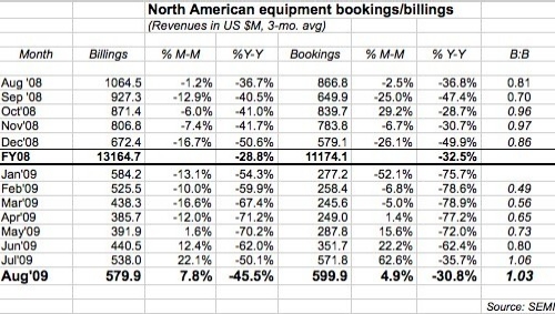
Worldwide bookings in North America came in at just under $600M in August 2009, a 5% improvement from July. Billings were about $580M, up nearly 8% from the prior month. And for both sides, yearly comparisons continue to improve, albeit slowly (bookings -31%, billings -45%), but far better than they were earlier in the year. And the book-to-bill ratio (B:B) held above the 1.0 parity mark at 1.03, meaning $103 worth of orders came in for every $100 worth of product billed for the month

Click to Enlarge

Some quick highlights:

  1. Back-to-back parity in the B:B, not seen in close to three years (Dec.06-Jan.07)
  2. Bookings growth: Five straight months of M/M growth, not seen since spring of 2006 (February-June)
  3. Billings growth: Four positive M/M months, not since spring of ’07 (March-June)
    Yearly comparisons are still ugly, but are now generally back in the same ballpark as they were in late 2008, the beginning of this mess — which suggests improvements will continue.

Equipment bookings have increased for five straight months and equipment sales are in the black for four straight; device sales and fab capacity utilization also have been improving, noted Stanley Myers, SEMI president/CEO, in a statement. And seeing the B:B ratio above the 1.0 parity mark for a second straight month generally indicates more business coming in than going out.

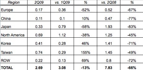
Another macro-sign of improvement: for the full quarter (2Q09) bookings/orders spiked 83% from 1Q09 to $2.95B; worldwide sales (which by definition trail bookings trends) were down only about -13% vs. the prior quarter to $2.69B. (Compared with 2Q08, bookings were down -58% and billings -66%, as if we needed reminding.) Such spending is comparable to what was seen in the early 1990s, noted SEMI’s Myers, in another statement.

And numbers are also brighter in Japan, where bookings (three-month moving average) rose about 27% from July to ¥55.46B (US ~$609M) and billings rose 17.6% to ¥38.57B ($423.6M). The Japanese B:B soared to 1.44 (vs. 1.34 in the prior month) to stay well above parity for the third straight month.

Click to Enlarge

Positive growth is certainly better than the alternative, especially in this new era where thinking quarterly, rather than annually, seems to be the preferred way to identify trends and shifts (and elicits the most optimism). August growth was quite a bit lower than the previous few months but perhaps that can be attributed to end-of-summer/midquarter/post-West/ doldrums. (Or maybe, as some have suggested, it’s indicative of a slight pullback among devicemakers/foundries.)

Sustained growth is certainly good, but it’s only part of the story — it’s going to take a long, hard push to get the industry back to a level of normalcy that’s sustainable for the industry overall, and for individual companies struggling to stay alive and compete. Gartner’s recent industry forecast update shows the spending rebound will crest in 2012 at about $50.3B, well below 2007’s level of $63.3B. IC Insights last week suggested the industry is committing a historically unprecedented 12% of sales to capex, and will stay in the low teens through 2013. What will the industry landscape do in the face of another year (or several) of discomfort? Time will tell — and maybe sooner rather than later.

by Debra Vogler, senior technical editor, Solid State Technology

September 15, 2009 –  Oxford Instruments Plasma Technology recently launched the Nanofab800 Agile system that provides development opportunities to influence the growth of nanostructures. With a process temperature up to 800°C, and agile heating and cooling for rapid turnaround, the system also delivers control of alignment and dimensions of the nanostructures.

Additional product features include variable sample sizes up to a maximum of 200mm wafers, temperature uniformity better than ±1.5%, and agile temperature control. According to Cigang Xu, development scientist at Oxford Instruments Plasma Technology, the rate of temperature increase for the new system can be up to 130°C/min and the cooling rate is up to 40°C/minute. "These rates are faster than typical values for PECVD tools, and allow the system to have rapid turnaround," said Xu.

The system is able to process at pressures up to 5Torr with a flow rate >1sl/m (standard liter/minute). "High pressure may allow the decrease of the process temperature," noted Xu. "For example, the Si nanowire can be grown at lower temperature when the pressure is higher." A high flow rate capacity also enables flexible choice on the process conditions.

The system is configured with a vacuum load lock to ensure process repeatability and chamber cleanliness and it has an optional liquid source delivery system. There is also a custom-developed setup for aligned growth and control of film stress. — D.V.

Click to Enlarge
Dense CNTs grown by the Nanofab800 Agile system. (Source: Oxford Instruments Plasma Technology)

September 10, 2009:  A procedure using nanotubes encased within DNA is shown to eliminate cancer tumors but not healthy tissue, according to researchers from Wake Forest U’s School of Medicine.

Their work, published in ACS Nano, starts by encasing multiwalled carbon nanotubes (MWNT) in DNA and injecting them into human prostate cancer tumors grown in mice. The DNA coating keeps the MWNTs dispersed in the tumor, allowing them to heat more evenly/efficiently (heat production increased 2x-3x), which means lower levels of radiation can be used.

Heating the tumor with near-infrared radiation (70secs with a 3W laser) causes the MWNTs to vibrate, creating heat which kills nearby cancer cells — in their work, the tumors were gone after six days. Tests on other treatment groups showed the combination of coated MWNTs and laser radiation was key; tumors that were only injected with MWNTs or irradiated by laser showed no distinguishable reduction.

From the ACS Nano abstract:

A single treatment consisting of intratumoral injection of MWNTs (100 μL of a 500 μg/mL solution) followed by laser irradiation at 1064nm, 2.5 W/cm2 completely eradicated PC3 xenograft tumors in 8/8 (100%) of nude mice.

Perhaps the most key result is that the surrounding tissue is "virtualy unharmed" — in tests "a small burn on the skin" at the site of the laser treatment healed in a few days with antibiotic ointment. Current "thermal ablation" (heat therapy) methods rely on heating implanted electrodes, which aren’t selective to cancer cells vs. healthy ones. "That we could eradicate the tumor mass and not harm the tissue is truly amazing," said principal investigator William H. Gmeiner, a professor of cancer biology at the School of Medicine, in a statement.

Future work will involve investigating whether other nanomaterials (e.g. single-walled carbon nanotubes or gold nanoshells) will work effectively. More investigation will be done to gauge long-term impact to the body in terms of toxicity — another reason to DNA-coat the CNTs, is to cautiously use fewer of them.