Category Archives: Materials and Equipment

May 26, 2011 — Camtek Ltd. (NASDAQ and TASE: CAMT) received repeat automatic optical inspection (AOI) orders from an Asia-based foundry doing advanced micro bump inspection and metrology.

Systems should be installed during Q2 and Q3 2011.

3D IC technology is trending to advanced micro bumps (>10mm), and may reach up to 1 million bumps per die. Microbumps allow increased device interconnects on a small package footprint. Challenges arise in measuring such small bumps, including efficiently handling huge amounts of data, said Roy Porat, Camtek’s CEO, who expects that this customer will order more in the future. Camtek’s AOI systems combine high performance 2D and 3D metrology and inspection on one platform.

Camtek Ltd’s automated tools enable inspection of semiconductors and printed circuit boards (PCB) & IC substrates, using intelligent imaging, image processing, ion milling and digital material deposition. Learn more at www.camtek.co.il.

Subscribe to Solid State Technology/Advanced Packaging.

Follow Advanced Packaging on Twitter.com by clicking www.twitter.com/advpackaging. Or join our Facebook group

by Mieke Van Bavel, science editor, imecClick to Enlarge

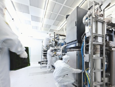
May 25, 2011 – The clock is ticking for EUV lithography, one of the main candidates to print critical layers in 22nm technology and beyond. According to Geert Vandenberghe, director of imec’s advanced lithography program, EUV will now have to prove its readiness, laying high expectations on ASML’s NXE:3100 preproduction tool, which is currently being installed at imec.

Nevertheless, he feels fairly secure about the tool’s capability. Already today, it produces a handful of wafers per hour, a 10× improvement compared to ASML’s alpha demo tool (ADT); this is expected to increase toward 60WPH by 1Q12. And from earlier tests at ASML, it seems that printing 22nm L/S comes within reach. Of course, besides tool development, mask defectivity and resist development remain in the top-3 of critical issues, but three years of on-site learning with the ASML ADT has enabled significant process. Take mask defectivity as an example. Some multilayer mask defects can currently only be found by wafer inspection techniques and you cannot repair them. But you can "mitigate" them (correct for their imaging effect), and imec has been able to do so. For resist, there is comparable good news.

Vandenberghe is convinced that all these issues have brought EUV closer to manufacturability. In parallel, his team is stretching 193nm immersion lithography to its ultimate limits to support technologies down to the 22nm node. They do this by co-optimizing scanner, process, and layout.

At next year’s imec ITF, we will rendez-vous to see if both technologies have met the expectations.

Click to Enlarge
ASML’s NXE:3100 tool being installed at imec.


by Dr. Paula Doe, SEMI Emerging & Adjacent Markets

May 24, 2011 – Alternative energy applications may help drive the power semiconductor market to $45 billion by 2014, according to IHS iSuppli. To meet their needs for more efficient high-voltage power management, growing markets like solar generation and vehicle electrification need are looking to GaN and SiC, innovative high-temperature packaging technology, and integrated process flows for integrating high voltage or RF with conventional CMOS. Analysts estimate better power electronics have the potential to reduce the world’s electricity consumption by some 20%-30% by 2025.

Demand for PV inverters will expand with the solar market to reach $4 billion by 2015, reports Yole Développement, while after about 2015 utilities will start investing in new high-end power management for more efficient distribution of electricity on the grid. Major automakers around the world are developing hybrids and electric vehicles, but a bigger market first is the increasing electrification of mainstream vehicles. The only way that future fuel efficiency and emissions standards can be met, especially in Europe, is by more electronically controlled smart power management, argues Cherif Assad, business leader for global power train and hybrid electric vehicles at Freescale Semiconductor — from systems that automatically turn the engine off and on instantly as the car stops and starts in city traffic, to electric motors that replace mechanical oil and water pumps.

Click to Enlarge
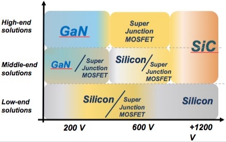
Technology positioning, 2015 forecast. (Source: Yole Développement, "Super Junction MOSFET" market report)

Power devicemakers see substrate technology as one key to better efficiency in many of these growing high-voltage markets, and are increasingly turning to SiC and GaN, but also to superjunction and neutron transmutation doped silicon. GaN-based power conversion devices are poised for commercialization, argues Tim McDonald, VP of emerging technologies at International Rectifier. "There will still be improvements from next-generation silicon, but we’re reaching the point of diminishing returns," he says. "So GaN is next." The company plans to introduce 600V GaN on Si devices later this year, and sees the potential for GaN based power conversion products to offer 2×-3× better performance/cost than existing silicon solutions. McDonald projects that 1%-2% of all power conversion applications will use GaN in 3-5 years.

Better high-temperature packaging without high costs is another key technology issue to solve, driven particularly by the demanding conditions of the electric and hybrid vehicle applications. Companies are replacing wire bonding with approaches that range from sintering to nanoparticle silver paste to eutectic bonding, as well as putting heat sinks on both sides of the die for double-sided cooling. "Packaging looks like the biggest opportunity now, the key enabler," says Laura Marlino, deputy director of the power electronics and electrical power system research center at Oak Ridge National Laboratory.

Also coming to the power electronics world is a new level of integration, potentially reducing size and costs and improving energy efficiency by combining high-voltage devices with other functions on the same chip in relatively conventional CMOS process flows. One example: IBM Microelectronics’ new foundry process combining high-voltage capability, CMOS logic control, and RF communication for smart wireless power management, aimed initially at enabling fine-grain smart wireless monitoring and control of PV systems. "The integration of HV and RF function on one piece of silicon represents a new paradigm," says James Dillon, from IBM’s Systems and Technology Group.

These hot topics in power semiconductor manufacturing technology will be the focus of this year’s program on emerging energy technologies at the Extreme Electronics TechXpot, Tuesday afternoon, July 12, featuring speakers from Freescale Semiconductor, Yole Développement, International Rectifier, SemiSouth, Oak Ridge National Lab, and IBM.

May 24, 2011 — Carsem, turnkey semiconductor packaging and test services provider, will grow its Suzhou, China factory by an additional 40,000 square meters (430,000 square feet). The additional space will allow Carsem to increase their Suzhou factory micro leadframe package (MLP) capacity from the current 5 million units per day to over 20 million per day, with a focus on copper wire bonding.

Click to EnlargeConstruction commenced in Q1 2011 and production operations are expected to begin in Q1 2012. The expansion will bring the total factory size to 56,000 square meters (600,000 square feet), with expanded test capability to match the new production output. Carsem expects to attract new potential customers with the capacity boost. 

The added assembly space will allot for increased copper wirebonding, along with traditional gold wire bond. Several packaging houses are moving to copper wire bonds for increasingly complex packages. MagnaChip Semiconductor now offers cost-competitive and state-of-the-art copper wire bonding technology and STATS ChipPAC Ltd. (SGX-ST: STATSChP) is investing in Cu wire bonding for finer silicon nodes (45/40nm) and low-k/extra low-k (ELK). Opponents consider gold wire to perform better than Cu wire, citing in-service product reliability, process yield, and "unproven performance."

Once completed, the Suzhou expansion will bring Carsem’s total MLP manufacturing capacity in both their Ipoh, Malaysia and Suzhou, China factory locations to over 26 million units per day.

Carsem MLPs are quad flat pack no-lead (QFN) and small-outline no-lead (SON) packages complaint to JEDEC MO220 and MO229 standards and are also offered with enhanced technologies such as copper-clip, flip-chip, system-in-package (SiP) and the 0.3mm-thick X3 form factor.

Carsem provides turnkey packaging and test services to the semiconductor industry, and offers a wide range of package & test services. Visit the website: www.carsem.com.

Subscribe to Solid State Technology/Advanced Packaging.

Follow Advanced Packaging on Twitter.com by clicking www.twitter.com/advpackaging. Or join our Facebook group

May 23, 2011 – Demand for semiconductor manufacturing equipment continues to inch up, with demand staying relatively steady as prior sales flush out the supply chain, according to data from SEMI.

For April, North America-based manufacturers of semiconductor equipment posted $1.598B in bookings, up 1.1% from February and about 11% higher than a year ago. Billings slipped -1.6% vs. March to $1.630B, but are still up 27% from a year ago (just a few weeks ago those Y/Y comparisons were 70%+). Both bookings and billings data in March were trimmed by about $40M from SEMI’s with preliminary results.

A look inside the April 2011 numbers:

  • Bookings are still holding steady at just below $1.6B, having added about $85M in the past few months to a seven-month high. "Current order and spending activity is aligned with announced 2011 capex plans," noted Dan Tracy, senior director of industry research and statistics at SEMI, in a statement.
  • Sales dropped about -1.6% in April to $1.63B. That’s a big improvement from the -10%/$180M [SEMI-adjusted] giveback seen in March. Generally it seems sales are simply passing earlier-digested demand — which would be good news, seeing how bookings/demand seem to be slightly increasing.
  • The book-to-bill ratio climbed again to 0.98, meaning $98 worth of orders received for every $100 billed. That means more business is going out (sales) than coming in (orders), and it’s almost back to the 1.0 parity mark. The climb in B:B is due to falling sales (-11% since February, from $1.84B down to $1.63B), though bookings have stayed relatively flat or up slightly (~$1.58B-$1.59B).


May 18, 2011 — Alchimer, nanometric film deposition provider for advanced 3D packaging applications, launched a new wet-deposition process, AquiVantage, that grows interconnect layers for interposer redistribution layers (RDLs) and significantly enhances via-last backside wafer interconnects. The process eliminates 2 costly photolithography steps.

Interposers incorporate a through-silicon vias (TSV) structure, as well as front-side redistribution circuitry (for attachment to the chip stack) and back-side redistribution and bumping (for attachment to the circuit board).

The AquiVantage process provides concurrent wet deposition of TSV and front-side isolation, barrier, and copper fill/RDL, while eliminating CMP and dry deposition steps. It also supports smaller vias with higher aspect ratios.

On the backside, the AquiVantage process allows selective maskless growth of the on-silicon isolation layer, completely eliminating an entire expose/develop/etch/clean lithography-process cycle.

AquiVantage uses the same cost-saving technology as Alchimer’s wet processes for TSVs.  It eliminates several process steps, including two costly photolithography steps, in producing high-quality films. By eliminating steps, 3D package interposer costs can be reduced 50%.

AquiVantage technology accommodates thicker wafers, eliminating the need for wafer carriers and allows for highly scalloped via structures and faster etching times.

Alchimer CEO Steve Lerner sees AquiVantage changing business models and fab methods of manufacturing enterprises all along the electronics value chain, including IDMs, OSATs, and foundries.

Alchimer develops and markets innovative chemical formulations, processes and IP for the deposition of nanometric films used in a variety of microelectronic and MEMS applications, including wafer-level interconnects and TSVs for 3D packaging. Visit www.alchimer.com.

May 17, 2011 Wafer bonding is a complex process, used on 2" to 12" wafers for MEMS, CMOS image sensors, advanced packaging, LEDs, and other chips. Yole Développement published a technology study and market research report, "Permanent wafer bonding," to derive trends in the market and technology through 2016. The report aims at analyzing the market perspectives and technical trends for permanent bonding.

Yole Développement has estimated that the wafer bonding market will grow significantly for the next year. The growth will be driven small-size wafers for LEDs and 12" wafers for 3D die stacking and CIS.

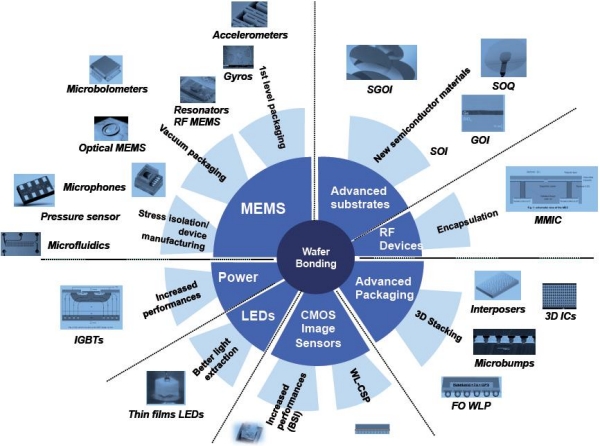
The wafer bonding market is a very complex one, crossing different wafer sizes (from 2" to 12"), different applications (MEMS, CMOS image sensors [CIS], LEDs, power devices, RF and advanced packaging), and different bonding technologies (adhesive, anodic, fusion, direct oxide, eutectic, glass frit, metal diffusion).
Click to Enlarge

Wafer bonding is usually defined as a process that temporarily or permanently joins two wafers or substrates using a suitable process. Historically developed for MEMS and then SOI wafers, wafer bonding technology has shifted to non-mainstream IC applications over the last years.

"MEMS has been the first application where wafer bonders have been massively used (the wafer bonding step is mostly used to protect the MEMS sensitive element), explained Dr Eric Mounier, project manager at Yole Développement. MEMS manufacturers are currently shifting from glass frit for eutectic/metal-based bonding, yielding smaller bond frames. Metal direct bonding also provides hermeticity and mechanical stability for many MEMS applications. For example, Nasiri uses eutectic bonding of the MEMS directly on the aluminum layer of the CMOS wafer. This leads to smaller package footprints & package heights. STMicroelectronics’ latest 3-axis accelerometer (LIS3DH) also shows a new sealing technique: gold eutectic sealing allows a dramatic die size reduction.

CMOS image sensors are also a strong wafer bonding application. Up to two different wafer bonding steps can be necessary for next-generation CMOS image sensor fab: one for back-side illumination, the second for wafer-level chipscale packaging (WLCSP). For CIS, the advent of backside illumination (BSI) technology has raised a competition between molecular bonding and adhesive bonding. Here, cost and final application will drive the final technology choice.

Besides MEMS and CIS manufacturing, wafer bonding also can be used for LED and power device fab. In a typical LED active region, spontaneous emission scatters photons in all directions. If the substrate material has a smaller band gap than the active region, approximately half of the light is absorbed in the substrate; significantly reducing device performance. So, one of the manufacturing solutions for photon loss involves bonding a wafer containing an array of devices to another wafer that provides both a reflective surface for maximum light extraction and a heatsink for thermal management.

Companies cited in the report:

Acreo, AML, APM/UMC, Avago, Ayumi, Bosch, Colibrys, Dalsa, Discera, EVGroup, FhG IMS, FLIR, IBM, Icemos, IMEC, IMT, Infineon, Infineon, Invensense, KTH, Leti, Lumileds, MEMStech, Micralyne, Mitsubishi Heavy Industries, Okmetic, Omron, Osram, Qualcomm, Raytheon, RPI, Sand9, Semefab, Sensonor, Silex, SOITEC, STM, SUSS MicroTEC, Tezzaron, TI, tMt, Tohoku University, TowerJazz, Tracit, Triquint, Tronic’s, TSMC, VTI, Xcom, Ziptronix

Over the 5 past years, much attention has been given to wafer bonding for 3D integration of memories, for example, and other die.

Although EV Group (EVG) is the market leader in permanent bonding, the growth of the bonding equipment market is attracting challengers.

Yole Développement’s report analyzes the technical & economical evolution of the permanent wafer bonding process. It gives 2010-2016 market forecasts for permanent bonding, equipment, an overview of the different bonding approaches and equipment players market shares and competitive information, This market & technology report also presents the trends for permanent bonding, wafer-to-wafer (W2W) vs. chip-to-wafer (C2W) analysis for 3D integration. It describes the applications for wafer bonding with main characteristics and challenges.
 
Report author:
Dr. Eric Mounier has a PhD in microelectronics from the INPG in Grenoble. Since 1998 he is a co-founder of Yole Développement, a market research company based in France. At Yole Développement, Dr. Eric Mounier is in charge of market analysis for MEMS, equipment & material. Yole Développement is a group of companies providing market research, technology analysis, strategy consulting, media in addition to finance services. Learn more at www.yole.fr

Subscribe to Solid State Technology/Advanced Packaging.

Follow Advanced Packaging on Twitter.com by clicking www.twitter.com/advpackaging. Or join our Facebook group

May 17, 2011 — Catalan Institute of Nanotechnology Professor Adrian Bachtold and his research group created resonators from nanoscale graphene and carbon nanotubes (CNT) that exhibit nonlinear damping. This result could lead to supersensitive detectors of force or mass.

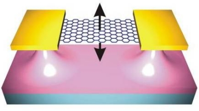
The team formed nanoscale resonators by suspending tiny graphene sheets or carbon nanotubes and clamping them at each end. These devices, similar to guitar strings, can be set to vibrate at very specific frequencies.

Click to Enlarge
Figure. A depiction of the nanoscale mechanical resonators constructed with graphene and CNTs. SOURCE: Catalan Institute of Nanotechnology.

Mechanical resonators mark time in electronic components and stabilize radio transmissions. In all mechanical resonators studied to date, from large objects several metres in size down to tiny components just a few tens of nanometers in length, damping has always been observed to occur in a highly predictable, linear manner.

Bachtold’s research demonstrates that this linear damping paradigm breaks down for resonators with critical dimensions on the atomic scale. The damping is strongly nonlinear for resonators based on nanotubes and graphene, a characteristic that facilitates amplification of signals and dramatic improvements in sensitivity.

Damping is central to the physics of nanoelectromechanical (NEMS) resonators, lying at the core of quantum and sensing experiments. Therefore many predictions that have been made for nanoscale electro-mechanical devices now need to be revisited when considering nanotube and graphene resonators. Prof. Bachtold’s group has achieved a new record in quality factor for graphene resonators and ultra-weak force sensing with a nanotube resonator, using these atomic-level devices.

Results will be published in Nature Nanotechnology (DOI 10.1038/NNANO.2011.71). To retrieve the abstract and full text, visit http://dx.doi.org/ DOI 10.1038/ NNANO.2011.71

Follow Small Times on Twitter.com by clicking www.twitter.com/smalltimes. Or join our Facebook group

May 12, 2011 — Researchers from the Technology Integration and Advanced Nano/microsystems (TIAN) Lab at the Department of Mechanical Engineering, University of Minnesota used IC assembly processes to fabricate single-walled carbon nanotube (SWCNT) composite thin film micropatterns and suspended beams. The stiff CNT-polymer composite thin film micropattern and suspended beam have potential applications to novel physical sensors, nanoelectromechanical switches, and other MEMS/NEMS devices.

Lithography-compatible layer-by-layer (LbL) nano-self-assembly was used to assemble negatively charged SWCNTs with a positively charged polydiallyldimethylammonium chloride.

The resultant composite thin film was patterned by oxygen plasma etching with a masking layer of photoresist, resulting in a feature size of 2µm.

The SWCNT nanocomposite stripe pattern with a metal clamp on both ends was released by etching a sacrificial layer of silicon dioxide in the hydrofluoric acid vapor. I-V measurement reveals that the resistance of SWCNT nanocomposite film decreases by 23% upon release, presumably due to the effect of reorientation of CNTs caused by the deflection of about 50nm. A high Young’s modulus is found in a range of 500-800GPa based on the characterization of a fixed-fixed beam using nanoindentation. This value is much higher than those of other CNT-polymer composites due to self-assembly and higher CNT loading.

The group was led by Tianhong Cui at the University of Minnesota. They have studied the lithography-compatible layer-by-layer nano self-assembly process in detail, and has previously configured nanomaterials as thin-film transistors and biosensors. The current work lends itself to nano-switches due to the thin films’ stiffness and electrical conductivity.

Dr Dongjin Lee was a PhD student when the study was conducted. He is currently a postdoctoral associate at the Korea Advanced Institute of Science and Technology (KAIST), Korea. The research group, TIAN Lab, is led by Prof. Tianhong Cui. The research goal of the group is to investigate the fundamental electrical and mechanical principles of new materials for MEMS/NEMS and low-cost micro/nanomanufacturing approaches, utilizing nanotechnology to effectively enhance the performance of micro/nanosystems. Learn more at http://www.me.umn.edu/labs/tianlab/.

Additional information including a detailed version of the fabrication procedure is available in the journal Nanotechnology. Access the article, "Suspended carbon nanotube nanocomposite beams with a high mechanical strength via layer-by-layer nano-self-assembly," here: http://iopscience.iop.org/0957-4484/22/16/165601

Follow Small Times on Twitter.com by clicking www.twitter.com/smalltimes. Or join our Facebook group

May 11, 2011 – BUSINESS WIRE — CoolChip Technologies won the MIT Clean Energy Prize for their technology that reduces data center cooling needs.

CoolChip helps data centers reduce cooling costs using patented technology to eliminate the thermal barrier that currently stifles the performance of a computer’s central processing unit (CPU). Comprised of a team of engineers and business professionals with extensive experience in information technology and thermo-mechanical engineering, CoolChip is dedicated to delivering the next generation of ultra-high efficiency air-based CPU coolers.

Other work on data center thermal management include hot-water cooling (IBM Zurich) and source-located thermal management (Nextreme Thermal Solutions).

CoolChip was selected from 80 teams from over 40 universities by prominent judges.

The MIT Clean Energy Prize is a national competition founded in 2008 by MIT, the U.S. Department of Energy and NSTAR to accelerate the pace of clean energy entrepreneurship and boost the clean energy economy.

Now in its fourth year, the MIT Clean Energy Prize is helping to jump-start the clean energy industry while creating jobs. In just three years it has helped form over two dozen companies that have already raised over $80 million in investment capital and research grants.

For additional information on the MIT Clean Energy Prize, please visit www.mitcep.org.

NSTAR is the largest Massachusetts-based, investor-owned electric and gas utility. For more information, visit www.nstar.com.

To learn more about Massachusetts Institute of Technology (MIT), visit www.mit.edu.

Subscribe to Solid State Technology/Advanced Packaging.

Follow Advanced Packaging on Twitter.com by clicking www.twitter.com/advpackaging. Or join our Facebook group