Category Archives: Materials and Equipment

May 11, 2011 — An international research team has discovered a new method to produce belts of graphene called nanoribbons. Using hydrogen, they have unzipped single-walled carbon nanotubes (SWCNT). The method also opens the road for producing nanoribbons of graphane, a modified and promising version of graphene.

As a conductor of electricity, graphene performs as well as copper. As a conductor of heat, it outperforms all other known materials. Variations of graphene properties could be acheived by making graphene in "belts" with various widths (nanoribbons). Nanoribbons were prepared for the first time two years ago, and can be produced by using oxygen treatment to unzip carbon nanotubes. However, this method leaves oxygen atoms on the edges of nanoribbons.

Click to Enlarge
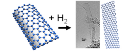
Figure. Researchers unzipped single-walled carbon nanotubes by using a reaction with molecular hydrogen.

In the new study, the research team shows that it is also possible to unzip single-walled carbon nanotubes by using a reaction with molecular hydrogen. Nanoribbons produced by the new method will have hydrogen on Click to Enlargethe edges, which can be an advantage for some applications. Alexandr Talyzin (pictured at left), physicist at Umeå University in Sweden, has over the past decade been studying how hydrogen reacts with fullerenes.

"Treating the carbon nanotubes with hydrogen was a logical extension of our research. Our previous experience has been of great help in this work," says Alexandr Talyzin.

Nanotubes are typically closed by semi-spherical cups, essentially halves of fullerene molecules. The researchers have previously proved that fullerene molecules can be completely destroyed by very strong hydrogenation. Therefore, they expected similar results for nanotube end cups and tried to open the nanotubes via hydrogenation. The effect was confirmed, and additional effects came to light.

Some carbon nanotubes were unzipped into graphene nanoribbons as a result of prolonged hydrogen treatment. Unzipped graphene ribbons with hydrogen attached to the side walls could possibly lead to synthesis of hydrogenated graphene: graphane. So far, graphane synthesis was mostly attempted by reacting hydrogen with graphene. This appeared to be very difficult, especially if the graphene is supported on some substrate and only one side is available for the reaction. However, hydrogen reacts more easily with the curved surface of CNTs.

Ilya V. Anoshkin, Albert G. Nasibulin, Jiang Hua and Esko I. Kauppinen at Aalto University are experts in the synthesis and characterization of singled-walled carbon nanotubes. Valery M. Mikoushkin, Vladimir V. Shnitov and Dmitry E. Marchenko from St. Petersburg made XPS and other characterization using synchrotron radiation. Dag Noréus at Stockholm University shared his expertise with high temperature hydrogen reactors.

The research was published in the journal ACS Nano:
Title: Hydrogenation, Purification, and Unzipping of Carbon Nanotubes by Reaction with Molecular Hydrogen: Road to Graphane Nanoribbons
Authors: Alexandr V. Talyzin, Serhiy Luzan, Ilya V. Anoshkin, Albert G. Nasibulin, Hua Jiang, Esko I. Kauppinen, Valery M. Mikoushkin, Vladimir V. Shnitov, Dmitry E. Marchenko, and Dag Noréus
Access it at http://pubs.acs.org/doi/abs/10.1021/nn201224k

Follow Small Times on Twitter.com by clicking www.twitter.com/smalltimes. Or join our Facebook group

by John Iacoponi, IITC/MAM conference general co-chair

IITC 2011
Day 2, 3 talks on process integration, reliability, 3Di
Sneak-peek at Day 1 talks
TSVs, beyond-CMOS top IITC-MAM "must see" lists for conference chairs
Imec CNT research: IITC preview
IBM’s double-exposure patterning creates BEOL interconnects beyond 22nm
Wet-process technologies for scalable through-silicon vias

May 12, 2011 – The joint 2011 International Interconnect Technology Conference (IITC)/Materials for Advanced Metallization Conference (MAM) conference continues in Dresden, Germany. Here’s a sneak peek at day 2 and day 3 talks.

Day 2, Tuesday May 10. Technical sessions included reliability, BEOL memory technologies, 3D integration, and interconnect process integration. Interconnect reliability has been a cornerstone topic at IITC since its inception and continues to be a very hot topic. Electromigration, stress migration, and time-dependent dielectric breakdown (TDDB) all remain top challenges, especially as dimensions continue to aggressively scale from node to node to enable chip scaling.

Continuing a trend started last year at IITC 2010, this year’s conference has a number of papers on BEOL memory technologies ranging from materials to integration to reliability. Another cornerstone of IITC has been process integration. Papers presented on Day 2 covered yield, ultralow-k, and self-aligned via/double patterning integration topics.

In an interactive, workshop-like format, over 60 posters were exhibited, giving the opportunity for direct one-on-one discussion with the presenters.

Day 3, Wednesday May 11. Leveraging the historical strength of the MAM conference, IITC Day 3 started off with several papers on materials and process technology, then shifted gears with a session on interconnects in the power and automotive marketplace. Wednesday afternoon IITC looked to the future, with presentations discussing graphene nanoribbons and carbon nanotubes (CNT) point to interconnect technologies beyond Cu/low-k. Day 3 ended with a session on metal gate materials and processes.

Continuing the IITC tradition of supplier partnership, several suppliers held technical seminars in the evening. On Monday, ASM International hosted a reception and seminar entitled "Bridging the gap to porous low-k," focusing on process and integration challenges toward k=2.0 materials. On Tuesday evening, Metryx hosted a similar event on the topic "A users perspective of mass metrology."

In 2012 the IITC will return to the San Francisco Bay area, completing an experimental four-year cycle alternating between US/Asia/US/Europe locations. The IITC organizing committee is evaluating continuing this rotation and looking into possible locations in Asia for 2013.

The IITC/MAM conference wraps up with Day 4 on Thursday May 12. The full technical program can be found on the IITC website.


John Iacoponi is technology research manager at Globalfoundries, and general co-chair of the IITC/MAM conference. Other co-chairs: Ehrenfried Zschech (Fraunhofer Institute), Takeshi Furusawa (Renesas Electronics), and Stefan Schulz (TU Chemnitz).

May 10, 2011 – Marketwire — RFaxis, a fabless semiconductor company focused on RF for wireless connectivity and cellular/mobility markets, released its patent-pending On-Die Coexistence Filter technology. When combined with RFaxis’ on-die transmit circuitry, the on-die coexistence filter helps reduce circuit board area, lower current consumption, and simplify bill of materials (BOM).

The packaging technology targets multifunction WLAN/Bluetooth/WCDMA cellular devices such as smartphones, tablets and other mobile internet devices.

"Conventional coexistence filters are bulky and expensive standalone components, and have always been a challenge for multifunction cellular device OEMs and ODMs in terms of lowering BOM costs, optimizing wireless performance and accelerating design cycles," stated Mike Neshat, chairman and CEO of RFaxis, who adds that On-Die Coexistence Filters eliminate an external companion component for the cellular RF front-end.

Dr. Oleksandr Gorbachov, RFaxis CTO, adds, "By integrating our new Coexistence Filter technology into our CMOS RFeIC single-die circuits for multifunctional cellular devices, RFaxis is able to reduce transmit power loss by at least 1.5dB at the antenna, significantly improve receive sensitivity, and substantially reduce current consumption by tens of milliamps. This translates into extended battery life and robust performance while saving PCB real estate."

RFaxis Inc. specializes in the design and development of RF semiconductor and embedded antenna solutions. More information can be found at www.rfaxis.com.

Subscribe to Solid State Technology/Advanced Packaging.

Follow Advanced Packaging on Twitter.com by clicking www.twitter.com/advpackaging. Or join our Facebook group

Peter Singer, editor-in-chief, Solid State Technology and ElectroIQ.com

May 9, 2011 — ElectroIQ’s chief editor Peter Singer recently toured the Center for Advanced Materials Processing (CAMP) at Clarkson University in Potsdam, NY. The Center is largely focused on the synthesis and processing of advanced materials. The following video interviews with researchers and professors cover particle transport, chemical-mechanical planarization (CMP), cleanroom technologies, and bright nano particles, among other topics.

Clarkson U research on particle transport

Goodarz Ahmadi, Dean of Engineering at Clarkson University (with the university for 30 years, Ahmadi has served as a dean for the past 5), discusses his research interests: particle transport in various environments, including particulate contamination in semiconductor manufacturing.

Ahmadi says: "We look at how particles are transported in various environments, such as in a room or in human respiratory systems. Also, we look a lot of industrial applications. I’ve done work with IBM, Xerox, Kodak, Corning and other companies, looking at issues that they had with particulate transport in various applications from copier machines to contamination of chip manufacturing systems. We’ve also done work for the NSF, NASA and the DoE related to energy issues."

CMP work at Clarkson U

S.V. Babu (also with the school for 30 years) discusses particle synthesis and chemical mechanical planarization (CMP) research taking place at Clarkson University. Babu has studied CMP for 15 years.

Babu says: "We have leveraged the expertise of CAMP in colloidal science and thin film processing. A lot of our students who have graduated are now running the CMP operations at IBM, Intel and Micron."

Bio-compatible ultra-bright fluorescent nanoparticle research

Igor Sokolov, Physics and Chemistry Professor at Clarkson University, shares info on ultra-bright nanoparticles that are substantially brighter than quantum dots.

Acoustics in engineering materials

Cetin Cetinkaya, Professor of mechanical engineering at Clarkson University, researches acoustics. Acoustic waves can be used to characterize drug function and effectiveness. Semiconductor nanoparticle removal can also be accomplished with acoustic waves.


Airborne particles and industry

Suresh Dhaniyala, Clarkson University, discusses airborne particles. These can be contaminants in the semiconductor fab. He shows us Clarkson U’s instruments to study particles.

More videos: See Clarkson professors discuss photovoltaics research here.

The visit was arranged by Tim Dunn, VP, marketing and business development, Mohawk Valley EDGE and the Marcy NanoCenter in Rome, NY and Mike Novakowski, director of business development, CenterState Corporation for Economic Opportunity, NY’s Creative Core in Syracuse, NY.  This was part of a tour of various prestigious universities in upstate New York (including Cornell University, Syracuse University and Binghamton University, as well the Syracuse Center of Excellence), with an eye on how well they could help businesses that decide to locate there.

Subscribe to Solid State Technology/Advanced Packaging.

Follow Solid State Technology on Twitter.com via editors Pete Singer, twitter.com/PetesTweetsPW and Debra Vogler, twitter.com/dvogler_PV_semi.

Or join our Facebook group

May 9, 2011 — The research project "MANOS" combines innovative surface coatings based on nanoparticles and the latest adhesive procedures for new embedding technologies and novel circuit-board-based modular fasten and release technology used to stack sensor systems.

Click to Enlarge

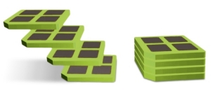
Figure. Single sensor modules can be stacked to create a sensor system via standardized interfaces.

MANOS is a research project supported by the German Federal Ministry of Education and Research (BMBF) called the "Modular Design of Systems with nanomodified Surfaces for Automotive and Industrial Sensor Technology." Companies have been involved in this project over a period of three years with the aim of promoting the development of modular sensor systems and meeting the standards of future products for increased functionality and greater robustness.

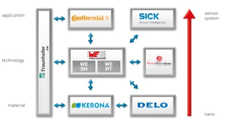
As project participants, the companies Continental, Delo Industrie Klebstoffe, Fraunhofer IZM, Kerona, RoodMicrotec, Sick and Würth Elektronik are contributing their core competencies for this project and thus adding to its innovativeness.

Kerona is developing nanomodified surface protection coatings that have various modifications. They make applications possible with optic sensors or temperature- and location-detection sensors.

Delo Industrie Klebstoffe is developing various adhesives that are needed for self-assembly of chips and for installing them in the circuit board, as well as for stacking the individual sensor modules. The adhesives will be responsible for electrical or thermal conduction.

— With embedding technologies such as "lasercavity" and "CHIP+," Würth Elektronik is contributing the significant experience it has acquired in embedding chips. This technology will be further enhanced with the use of innovative adhesives and new surface coatings. The aim is to develop new fasten and release technologies based on circuit boards, make them capable of series production, and optimize their manufacturing to reduce costs.

Roodmicrotec is responsible for evaluating the processes by means of brief certification procedures and reliability inspections of the sensor systems. Special emphasis is given here to standardizing the certification policies.

Continental and Sick are using the sensor systems in various areas. Continental builds multi-sensor systems for automotive transmission controls. Sick produces industrial optical miniature sensors and sensor systems. Continental and Sick thus face different kinds of challenges in terms of usage, but they both have one thing in common: the focus on standardizing the interfaces in terms of cost effectiveness.

Fraunhofer IZM is supporting all project partners in its basic research, laboratory investigations and theoretical approaches.

Click to Enlarge

Chart. Company relations.

Nanostructured and nanomodified surface coatings will help create new fasten and release technologies based on circuit boards and thus open new paths for innovative modular system designs. The modular structure allows users to connect conventional sensors with each other by means of standardized interfaces and combine them to form new sensor systems. Such modular designs for complex miniaturized multi-sensor systems are an alternative to isolated applications and they enable much shorter innovation cycles of systems for various requirements.

There is a great variety in possible uses: automotive or industrial sensory systems, medical technology, etc.

Subscribe to Solid State Technology/Advanced Packaging.

Follow Advanced Packaging on Twitter.com by clicking www.twitter.com/advpackaging. Or join our Facebook group

May 9, 2011 — Pyrograf Products Inc.’s quality management system has been ISO 9001:2008 certified. In the growing field of carbon nanotube (CNT) manufacturers, ISO certification provides essential customer confidence and company credibility, states Pyrograf Products.

Pyrograf Products developed quality control methodologies for the commercial scale production of stacked-cup carbon nanotubes (CNT), also known as carbon nanofiber. The company recently consolidated 15 years of carbon nanotube quality control experience and expertise into a quality management system and was granted ISO 9001:2008 certification.

ISO 9001 provides a suite of proven business and quality management techniques to efficiently and effectively operate a successful business. Pyrograf Products developed its quality management system according to ISO standards over a one-year period and then underwent a thorough analysis of its policies and procedures conducted by Eagle Registrations Inc. Eagle, based in the Dayton, OH area, is an ANSI-ASQ National Accreditation Board (ANAB) accredited registrar.

Certification through Eagle to ISO 9001:2008 ensures consistent quality and continual improvement of products to provide an added sense of confidence in Pyrograf-III carbon nanofiber, says Pyrograf. "ISO certification provides an internationally recognized means for us to communicate Pyrograf’s commitment to quality and continuous improvement to our customers," said David Burton, GM.

Pyrograf-III is a patented, highly graphitic, low-cost stacked-cup carbon nanotube with properties approaching the theoretical values of graphite in almost every performance characteristic. Pyrograf-III stacked-cup carbon nanotubes are a highly pure product with over 99.9% fibrous material and very low metal concentrations. Pyrograf Products produces stacked-cup carbon nanotubes with an annual capacity of 50,000 lbs per year. Pyrograf-III stacked-cup carbon nanotubes are currently being used worldwide to provide mechanical, electrical, and thermal advantages in polymeric composites.

Also read: CNT, graphene, and other nanocarbon production lags capacity 

Pyrograf Products, Inc., an affiliate of Applied Sciences, Inc., was incorporated in 1996 to manufacture carbon nanofiber in commercial volumes under the trade name Pyrograf-III. Applied Sciences, Inc. (ASI) has developed a national reputation as a research organization specializing in advanced materials and their applications. Learn more at http://pyrografproducts.com

Follow Small Times on Twitter.com by clicking www.twitter.com/smalltimes. Or join our Facebook group

By Debra Vogler, senior technical editor

May 4, 2011 — Anticipating a lively discussion at this year’s combined IITC-MAM conference (May 9-12, 2011, Dresden, Germany), www.Electroiq.com reviewed some of the "hot button" issues in a podcast with Michael Armacost, IITC publicity chair, and managing director, etch, at Applied Materials; John Iacoponi, IITC conference chair, and senior manager, technology research, at Globalfoundries; and Dorel Toma, IITC program chair, and director of U.S. technology development at TEL.

More IITC previews:

Armacost offered up three hot topics to watch for at the conference. The first is how the industry can deal with increasing RC performance in backend of line (BEOL). "This is the core of the conference," said Armacost. "And this issue is getting more critical as dimensions shrink and the space to put a conducting film is getting smaller and smaller." Among the approaches to address this issue: increasing the dielectric constant of the film, and reducing the resistance of the lines themselves. Also critical is tying together different functions through packaging strategies such as through silicon vias (TSV). A third topic is carbon interconnects and how they might be used as features continue to shrink. "And in memory, there is a lot of interest in how you integrate into the front end with contacts, and in memory cells that need to be integrated into the back end, whether it’s resistive RAM (RRAM) or other methods."

Dorel Toma reminds listeners that IITC is now combined with the MAM conference. "We are looking for post-CMOS technology (i.e., the end of the ITRS roadmap) using carbon technology for very small geometries/pitch sizes," he said. There will be a few important papers that "aggressively discuss integration of carbon-based materials (e.g., carbon nanotubes (CNTs), graphene), as well as hybrid integration (potential connection between "classical" copper and carbon-based materials)." Toma cited one paper in particular that will be presented by imec’s N. Chiodarelli ("Carbon nanotube interconnects: electrical characterization of 150nm CNT contacts with Cu damascene top contact"). Listen to imec discuss the paper here. The imec paper will cover electrical data obtained from the automated probing of 150nm diameter contacts filled with CNTs connected by a Cu damascene top contact module. The researchers note that the data represent a significant step forward toward the realization of CMOS contact modules with CNT interconnects.

 Click to Enlarge  Click to Enlarge
 

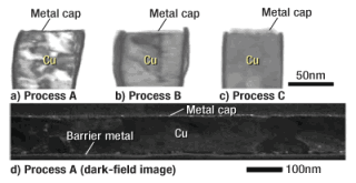
Figure 1. Cross-sectional TEM images of metal caps on 66nm wide Cu lines for three different processes: a) process A with 5nm-thick and full coverage; b) process B with <3nm-thick and partial coverage; c) process C with 8nm-thick and partial coverage; and d) a dark-field image along with the line direction with the metal cap "A."

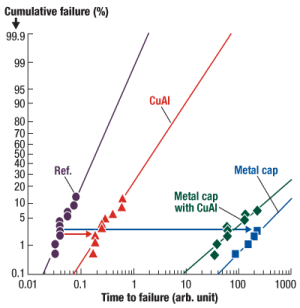
Figure 2. Distributions of EM lifetimes for the metal cap "A" and the CuAl-alloy lines. — 350°C 20MA/cm2

In his interview, John Iacoponi mentions some interesting papers on the conference’s core traditional topics: issues ranging from metallization and reliability (e.g., Ueki/Renesas, "Effects of metal-cap coverage on electromigration (EM) tolerance for scaled-down Cu interconnects") to an increased focus on not just the RC aspects of interconnects, but how one can pattern smaller structures with the existing immersion lithography tools. "There are several papers about dual-damascene interconnects using pitch-splitting technology," said Iacoponi. "The Renesas paper is pushing the limits of electromigration by studying the effects of metal cap coverage (Figs. 1 and 2)." There are several papers that talk about advanced barrier materials, including some work on self-formed barriers that have been in discussion in the industry but haven’t necessarily taken off, noted Iacoponi.

Click to Enlarge

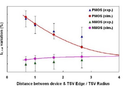
Figure 3. Idsat shift in the [-110] direction for pMOS and nMOS devices.

Armacost added that the conference chairs reviewed some papers on TSVs that indicate practical, tangible results. "TSMC has a paper on the impact of TSVs on devices themselves (Hsieh/TSMC; "Orthotropic stress field induced by TSV and its impact on device performance;" (Fig. 3)," said Armacost. "And in the CNT paper Dorel mentioned, we’re starting to see how you can put TSVs into an integrated structure. I think that’s what will set some of the papers apart this year."

Click to EnlargePodcast: Play Now or Download  

  • Format: mp3
  • Length: 9:06
  • Size: 8.33 MB
  • Date: 05/04/11

May 4, 2011 — A team of researchers at MIT has found a way to manipulate both the thermal and electrical conductivity of materials by changing the external conditions. The technique can change electrical conductivity by factors of well over 100, and heat conductivity by more than threefold.

Researchers used percolated composite materials and manipulated them by controlling their temperature.

Click to Enlarge

Image. An artistic rendering of the suspension as it freezes shows graphite flakes clumping together to form a connected network (dark spiky shapes at center), as they are pushed into place by the crystals that form as the liquid hexadecane surrounding them begins to freeze. SOURCE: Jonathan Tong.

The researchers suspended tiny flakes of one material in a liquid that, like water, forms crystals as it solidifies. For their initial experiments, they used flakes of graphite suspended in liquid hexadecane, but they showed the generality of their process by demonstrating the control of conductivity in other combinations of materials as well. The liquid used in this research has a melting point close to room temperature but the principle should be applicable for high-temperature use as well.

The process works because when the liquid freezes, the pressure of its forming crystal structure pushes the floating particles into closer contact, increasing their electrical and thermal conductance. When it melts, that pressure is relieved and the conductivity goes down. In their experiments, the researchers used a suspension that contained just 0.2% graphite flakes by volume. Particles remain suspended indefinitely in the liquid, as was shown by examining a container of the mixture three months after mixing.

By selecting different fluids and different materials suspended within that liquid, the critical temperature at which the change takes place can be adjusted at will, said Gang Chen, MIT’s Carl Richard Soderberg Professor of Power Engineering and director of the Pappalardo Micro and Nano Engineering Laboratories.

The system that Chen and his colleagues developed could be applied to many different materials for either thermal or electrical applications. One potential use of the new system, Chen explains, is for a fuse to protect electronic circuitry. In that application, the material would conduct electricity with little resistance under normal, room-temperature conditions. But if the circuit begins to heat up, that heat would increase the material’s resistance, until at some threshold temperature it essentially blocks the flow, acting like a blown fuse. Instead of needing to be reset, as the circuit cools down the resistance decreases and the circuit automatically resumes its function. Heat switches exist, but involve separate parts made of different materials, whereas this system has no macroscopic moving parts, says Joseph Heremans, professor of physics and of mechanical and aerospace engineering at Ohio State University.

Another possible application is for storing heat, such as from a solar thermal collector system, later using it to heat water or homes or to generate electricity. The systems much-improved thermal conductivity in the solid state helps it transfer heat.

"Using phase change to control the conductivity of nanocomposites is a very clever idea," says Li Shi, a professor of mechanical engineering at the University of Texas at Austin. MIT is interested in developing other applications for the process now.

Gang Chen, MIT’s Carl Richard Soderberg Professor of Power Engineering and director of the Pappalardo Micro and Nano Engineering Laboratories, is the senior author of a paper describing the process that was published online on April 19 http://www.nature.com/ncomms/journal/v2/n4/full/ncomms1288.html and will appear in a forthcoming issue of Nature Communications. Lead authors are former MIT visiting scholars Ruiting Zheng of Beijing Normal University and Jinwei Gao of South China Normal University, along with current MIT graduate student Jianjian Wang.

The research was partly supported by grants from the National Science Foundation.

Learn more at http://web.mit.edu/

Follow Small Times on Twitter.com by clicking www.twitter.com/smalltimes. Or join our Facebook group

May 4, 2011 – MarketwireSTATS ChipPAC Ltd. (SGX-ST: STATSChP), semiconductor test and advanced packaging service provider, has shipped over 300 million semiconductor packages with copper wire-bond interconnects. The SATS provider is investing in Cu wire bonding for finer silicon nodes (45/40nm) and low-k/extra low-k (ELK).

STATS ChipPAC is investing in equipment and resources to support copper wire technology in wafer nodes down to 45/40nm with low-k and ELK dielectric materials. Development work is focused on finer bond pad pitches, thinner wire diameters, stacked die packaging and die-to-die bonding, each of which represents a greater set of challenges in the application of copper wire.

The transition from gold to copper wire interconnect in semiconductor packages offers a significant savings in material costs while meeting electrical and thermal performance characteristics with quality and reliability standards that are comparable to gold wire, the company states. STATS ChipPAC has copper wirebond capabilities in all five of its manufacturing facilities in Asia, each with class 1000 cleanroom environments.

Production volume has been rapidly increasing in both leadframe and laminate packages. "We are in high-volume manufacturing for a large number of devices across multiple factories and have built significant momentum on the engineering front to introduce copper wire into a wider range of applications in the communication, computing and consumer markets," said Hal Lasky, EVP and chief sales officer, STATS ChipPAC.

"We are successfully addressing many of the technical challenges that are associated with using copper wire interconnect in more complex package structures. We have been aggressively developing copper wire capabilities in all our factories and rapidly expanding into a broader range of fine pitch devices and advanced silicon nodes. Our dedicated resources, especially our strong global copper wire engineering organization, ensure a consistent and successful transition to copper wirebond for our customers," said Dr. Han Byung Joon, EVP and chief technology officer, STATS ChipPAC.

STATS ChipPAC Ltd. is a leading service provider of semiconductor packaging design, assembly, test and distribution solutions in diverse end market applications including communications, digital consumer and computing. With global headquarters in Singapore, STATS ChipPAC has design, research and development, manufacturing or customer support offices in 10 different countries. STATS ChipPAC is listed on the SGX-ST. Further information is available at www.statschippac.com

Also read: Cu wire bonding joins MagnaChip Semiconductor offerings

K&S: Enabling high-volume fine-pitch Cu wire bonding

Subscribe to Solid State Technology/Advanced Packaging.

Follow Advanced Packaging on Twitter.com by clicking www.twitter.com/advpackaging. Or join our Facebook group

by Michael A. Fury, Techcet Group

Click to EnlargeMay 3, 2011 – The final day of the MRS Spring 2011 meeting was more like a regular wake than the Irish wake of the preceding four days, in that everyone had been high on data (and caffeine). On Friday, the halls were quite a bit more subdued, perhaps due to exhaustion. The upside of the diminished crowd was that the coffee did not run out halfway through the break. I applaud the 25 hearty souls who persevered through the last talk of the last symposium on the last day.

My movement between rooms afforded me the opportunity to visit the coffee urns on both meeting floors of Moscone West during the break. To my surprise, one floor was apparently serving Starbucks, while the other was serving Seattle’s Best. Was this a deliberate distribution of wealth among suppliers? Or a subtle class distinction between floors? Inquiring minds had to know, so I asked the head barista. It turns out that one floor used the wrong labels. (In the interest of global peace, I will not reveal which label was in error.) My own taste test confirmed that the beverages were the same, and well within acceptable parameters.


(Additional presentation details can be found online on the MRS Spring 2011 abstracts page. The underscored codes at the beginning of papers reviewed below refer to the symposium, session, and paper number.)

Interconnects and optoelectronics

Wim Bogaerts at IMEC (O10.1) opened the emerging interconnect technologies session with a review of optical interconnects for photonic devices, the primary driver being our insatiable thirst for bandwidth. Light slows down in matter in proportion to the refractive index, so lower refractive index materials are desirable to make the speed of light faster! To calibrate, we’re looking at an available bandwidth of 40THz. Silicon photonics has a scattering loss from sidewall roughness of ~1dB/cm (~50% loss per inch) but this is adequate so far for on-chip applications. High speed signal modulators for silicon photonics requires introduction of a perovskite, Ge or polymer material to operate in the 42Gbit/sec range. Photonic layers are notoriously temperature sensitive and will likely require local temperature regulators, raising a serious issue of power management.

MRS Spring 2011
Day 1: Lighting the paths for LED materials
Day 2: The III-V future of CMOS, the return of spin-on low-k
MRS Day 3: Memory, hardmasks, low-k — nothing’s confidential
MRS Day 4: Outside CMOS fabrication, but respecting boundaries
MRS Day 5: Opto, interconnects, organics, Borg?
Thin-film PV materials under the microscope @ MRS

Dunlin Tan from Nanyang Technological U. (O10.2) introduced their scheme for the use of vertically aligned carbon nanotubes (CNT) for flip-chip interconnects. A TiN barrier layer is needed to separate the metallization from the CNT catalyst for good growth without consumption or contamination of the metallization. The chosen scheme calls for a CNT-to-CNT bond between the chip and substrate, rather than CNT-to-metal.

In an effort to achieve zero-emission data computer centers, Gerhard Meijer of IBM Zurich (I11.5) decided to cool supercomputers with hot water instead of cold water. (I know what you’re thinking, but wait…) Server centers consumed 2% of global electrical power generated in 2009. Only 47% of that is consumer by the IT equipment itself, much of it driven by leakage current at those 5nm gate oxides; the rest is spent on air conditioning. Micro-channel liquid coolers fabricated in silicon would operate with a much smaller temperature gradient between the inlet water and CPU temperature. The cooling system picks up 85% of the heat generated when operating at 60°C. Net energy consumption for the prototype data center was reduced by 40%. The first commercial implementation is planned later this year for the 3PFLOPS HPC supercomputer center in Munich. The concept is being extended in PowerPoint space to interlayer liquid cooling for 3D CPU stacking. Calculations indicate an extraction capability of 7.2kW from a 10-layer CPU stack in a 4cm2 footprint.

Kris Bertness at NIST (EE10.1) showed a method for growing GaN nanowires without the use of a catalyst, which would constitute an impurity that ultimately degrades its optoelectronic properties. The wires are shown to lase with n type background carriers in undoped materials at a concentration of <1^1016cm-3. Good electroluminescence was observed in p material. The only successful p type dopant for GaN is Mg and it tends to form tapered nanowires rather than ones with a uniform thickness. She discussed a number of assumptions used for modeling of planar materials that give grossly incorrect results when applied to nanowires.

Cengiz Ozkan at UC Riverside (O10.5) explored the use of graphene and InSb nanowires for nanoscale interconnects. Graphene has the bonus property of being an effective heat spreader, and showed a sustained data transmission capability of 90Mbit/sec. This is still far from competitive with the 2.5Gbps rate of Cu over a 20cm length. The InSb wires demonstrated 10Mbit/sec without any impedance matching. Additional improvement of the CVD methods used to deposit these films is underway.

Won Lee of Sungkyunkwan U. (O10.6) used graphene interconnects to demonstrate stretchable silicon TFT ICs on a rubber substrate. The devices functioned well up to 10% stretching, limited by the particular epoxy used in their demonstration.

Nobuhiko Kanzaki from Santa Clara U. (O10.7) sought to reduce the contact resistance between FIB- and e-beam-deposited tungsten contacts and carbon nanofiber (CNF) interconnects and vias. Resistance between Au electrodes dropped from the 100MΩ range to the 10kΩ range with the use of their W contact. Comparable resistance behavior was found between the two contact deposition methods after the e-beam method was optimized. E-beam has the advantage of lower operating energy, thus less potential damage to the underlying materials.

Kyongjun Kim at Seoul National U. (O10.8) demonstrated the use of patterned solution-processed ZnO films for transparent thin film transistors (TTFTs). Conventional lithography and plasma etching are not friendly to ZnO. They define the pattern in PMMA, then spin coat a ZnO solution to fill the features. The device is then immersed in a toluene/methanol solvent that extracts water from the ZnO features and stabilizes them for subsequent annealing at 200°C. Electrical performance was within the target ranges.

Life sciences applications

Cecile Delacour of Institut Néel-CNRS, Grenoble (EE11.1) demonstrated the use of a Si FET array to detect charge propagation in neuron circuits. Seeing these alien creatures on an otherwise pristine silicon surface made my contamination engineer neurons fire stochastically, but the technique does lend credence to the origin of the Borg. This work has serious implications for the understanding of neurological disorders such as Parkinson’s disease. Sensitivity and selectivity were further enhanced by incorporating 100nm Si nanowires into the system.

Ping Xie from Charles Lieber’s group at Harvard (EE11.2) fabricated a nanowire-nanopore FET sensor for detecting DNA translocation. This is the first FET-based nanopore sequencing device and the first multiplexing sensor detection of translocation.

Rouxue Yan of UC Berkeley (EE11.3) developed a technique for single cell endoscopy using SnO2 nanowire wave guides. Such a device can facilitate selective targeting for gene or drug delivery, intracellular imaging, and sensing of molecular dynamics processes within the cell. The micromanipulator employed can control the position of the probe tip with a precision of 100nm. Using conical glass nanoprobes results in cell death in a minute or less, whereas cells survive five minutes or more with these nanowire Cells exhibit a high tolerance to rapid injection or short-term interrogation, with 85% of the cells recovering fully after withdrawal. Unlike their multi-cellular human counterparts, individual cells require neither anesthetic nor medical insurance coverage to undergo the procedure. Getting a signature on the medical waiver form is a challenge that remains to be addressed.

Organic devices

Tau-Hun Ha from U Texas @ Austin (OO17.5) fabricated p channel organic polymer TFTs based on diketopyrrolopyrole-naphthalene copolymer (PDPP-TNT) which has a mobility of ~1cm2/Vsec. Performance in dual gate mode was superior to single gate mode. Morphology studies vs. annealing temperature were used to explain changes in device switching response times due to inhomogeneous crystallization.

Omar Khatib at UC San Diego (OO17.6) studied the infrared signatures of ambipolar charge injection in donor-acceptor copolymer OFETs. These devices were fabricated with PBBTPD on n doped Si for ease of analysis for the purpose of studying the fundamentals of ambipolar charge transport in this class of materials. This work represents the first IR signatures of ambipolar behavior.

Fabrice Mathevet from U. Pierre et Marie Curie, Paris (OO17.7) described his studies on molecular and macromolecular semiconducting liquid crystals intended for OFET and PV applications due to their high carrier mobility. Synthesis pathways and structural characterization were described for several compounds.

Toby Nelson of CMU (OO17.8) aspires to fabricate inexpensive throwaway devices for RFID and comparable applications using a ‘transistor paint’ comprising a next-generation set of material based on DTP and DPP, with early work reported on PDDTP-DPP. Device mobility with this material was as high as 0.41cm2/Vsec is highly repeatable and quite stable in normal environmental handling.

Christian Nielsen of Imperial College London (OO17.9) discussed his work on trithienobenzene-based polymers for high-performance FETs and OPVs. The materials have good absorption in the 500nm-600nm range. Mobilities on the order of 0.3cm2/Vsec were achieved for some of the compounds explored.

Toshihiro Okamoto from the U. of Tokyo (OO17.10) focused on the synthesis of face-to-face Π-Π stacked structures using fused acene backbones. A strategy of alternating aryl and perfluoroaryl was adapted to affect more aggressive stacking interaction. Time-resolved microwave conductivity was used to evaluate photoconductivity of single crystals of the material synthesized. The molecular design formalism proved promising, but outstanding mobility results have yet to be achieved.

Atefeh Yousefi Amin at the U. of Erlangen-Nurnberg (OO17.11) fabricated high mobility (6.4cm2/Vsec) OTFT devices based on 2,7-dialkyl-[1]benzothieno[3,2-b][1]benzothiophene (BTBT), resulting in a p channel transistor. Operating voltage was reduced by using a 5nm Al2O3 with a fluorinated SAM to adjust the threshold voltage from -1.8V to -1.1V (compared to -14V with an SiO2 gate dielectric).

Ajay Perumal of Technische Universität Dresden (TUD) (OO17.12) showed feasibility for alternating current OLEDs using doped organic semiconductors. A luminance of 1000Cd/m2 and a maximum efficiency of 0.37 lumens/W were achieved with the device, which does not respond to DC voltage. The luminance is attributed to the charge carrier generation and recombination, leading to formation of excitons within the device, without the injection of charge carriers through the external electrodes.


Michael A. Fury, Ph.D, is senior technology analyst at Techcet Group, LLC, P.O. Box 29, Del Mar, CA 92014; e-mail [email protected].