Category Archives: Materials and Equipment

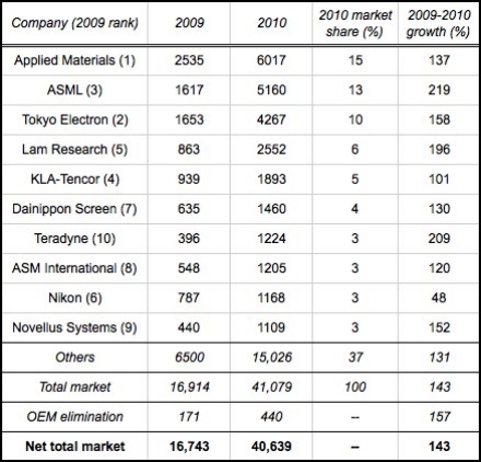
April 11, 2011 – Global semiconductor capital equipment spending raced ahead 143% in 2010 to $41.08B (including some OEM contributions), according to Gartner. Sales growth was slightly better for wafer-fab equipment (WFE, 145%) and automated test equipment (ATE, 149%), and slightly less for packaging/assembly equipment (PAE, 127%). Top growth goes to litho supplier ASML (219% growth to $5.16B), followed by test supplier Teradyne (209% growth to $1.22B) and etch stalwart Lam Research (196% to $2.55B).

(The numbers are largely in line with what VLSI Research reported recently, though the Gartner numbers show some differences further down the list: Nikon at No.9 [VLSI showed Nikon slipping off its top-10 list] and Novellus at No.10 [ranked ninth by VLSI].)

Some key trends illustrating capital spending in the year 2010:

Technology, then capacity. Why was 2010 such a good year? Because it managed to incorporate both drivers of capital equipment spending, according to Klaus Rinnen, Gartner managing VP, in a statement. Those with memory and foundry exposure also did particularly well.

Litho: A double-patterned sword. ASML hiked up the list thanks to demand for immersion lithography systems for double patterning, increasing to 13% market share overall. However, "strength in double patterning benefited some companies more than others," Rinnen noted. (Hello, Nikon.)

Big get bigger. Applied Materials more than doubled sales in 2010 to top $6.0B — but still couldn’t pick up market share, as other sectors (e.g. litho) expanded more rapidly. For the same reason, TEL dropped a spot to No.3 despite its dominance in track, and also thanks to "relatively slower spending by some of its key customers," Rinnen noted. Overall, though, the top 10 suppliers picked up nearly two points to account for 63.4% of total revenue.

Click to Enlarge
Top 10 companies’ revenue from shipments of total semiconductor equipment, worldwide (in US $M). (Source: Gartner)

Clearly the massive and tragic earthquake + tsunami disaster in Japan is having a near-term impact on many industries, including semiconductors, for two main reasons: lack of reliable infrastructure/power, and shortages of components and materials (e.g. BT resin and silicon). This will be a challenge in the coming few months, but "semiconductor equipment manufacturers should be able to recover in the second half of the year," Gartner thinks.

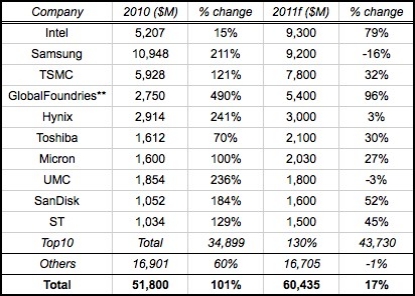
In fact, another analyst firm thinks 2011 will raise the capex roof significantly vs. 2010 even taking the Japanese disaster into account. IC Insights has boosted its capex forecast to 17% ($60.4B), and then even higher in 2012 to $63.3B. Foundries will be adding manufacturing lines and technology upgrades in response to more business from IC suppliers, and memory suppliers simply need to relentlessly push to the next process geometries.

It’s worth noting that every cent of capex growth in 2011 is coming from the top-10 spenders: 25% growth to $43.7B, vs. a -1% decline in spending from everyone else. Note that Samsung, whose jaw-dropping $10.9B spending in 2010 was more than a fifth of total semiconductor spending — and nearly that of Intel and TSMC combined — will pull back to "only" $9.2B in 2011, with 56% of that going to memory (vs. 71% in 2010). Put those together and Samsung is shelling out more than $20B in two years — equivalent to five leading-edge 300mm wafer fabs ($4B a pop).

While the numbers for 2010 seem massive, IC Insights thinks it wasn’t excessive spending, as most of it was for technology-ramping rather than capacity additions. Capex as a percentage of sales was just 16%, the second-lowest on record; 2011 capex/sales will be just 17%, IC Insights forecasts. (For reference, capex/sales was around 26% in the late ’90s and through the 2001 downturn, and ~20% from 2003-2009.) The firm projects this low spending ratio will continue through 2012 and beyond, at 14%-17% capex/sales over the next five years.

Click to Enlarge
2011 top spenders’ semiconductor capital spending (including company’s share of joint-venture spending). **Includes Chartered for 2010. (Source: IC Insights, company reports)


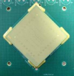
April 7, 2011 — Zymet Inc. introduced a reworkable edgebond adhesive, UA-2605, that improves thermal cycle performance of CBGAs and plastic BGAs.

In one trial, UA-2605 tripled the 0°C to +100°C performance of a CBGA, to nearly 2500 cycles. Previously, underfill was needed to achieve this level of performance, Zymet says.

Click to Enlarge
Figure 1. Edgebonded CBGA.

The edgebond adhesive is easier to process than an underfill. When applying underfill, the printed circuit board (PCB) is preheated to facilitate capillary flow, and multiple dispense passes are used to deposit sufficient material. With UA-2605, only four beads of the adhesive are required, one at each corner. There is no need to preheat the PCB, wait for underfill flow, and make multiple dispensing passes.

Click to Enlarge

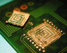
Figure 2. After removal of underfilled BGA, underfill residues must be removed.

Reworking an underfilled BGA is a time consuming and delicate task. Underfill residues must be removed and, for fine-pitch BGAs, the risk of pad damage is high. With UA-2605, BGA rework is simple and straightforward. The temperature is raised and the adhesive is scraped away; then, the BGA is reflowed and lifted from the board. Little site cleaning is necessary.

Zymet is a manufacturer of microelectronic and electronic adhesives and encapsulants. Its products include die attach adhesives, substrate adhesives, UV curable glob top and cavity-fill encapsulants, and underfill encapsulants.

For more information, visit www.zymet.com.

Subscribe to Solid State Technology/Advanced Packaging.

Follow Advanced Packaging on Twitter.com by clicking www.twitter.com/advpackaging. Or join our Facebook group

April 7, 2011 – FARS News Agency — Iranian researchers at Mashhad’s Ferdowsi University improved the quality of microextraction by incorporating carbon nanotubes (CNTs).

"We studied trace measurements of environmental samples by gas-liquid chromatography method and applying a new pre-concentration method," Dr. Sarafraz Yazdi, professor at Ferdowsi University, told INIC.

Pre-concentration (extraction) methods demand high consumption of organic solvents, which are expensive and pollute the environment. Scientists have been working on microextraction methods that need no or little amounts of solvent since the 1990s. "One of the non-solvent methods is solid phase microextraction (SPME) in which some solid phase adsorbent (of micrograms) is placed on a capillary fiber of melted silica. This fiber is exposed to the sample and adsorbs it. Afterwards, desorption process takes place in measurement device," Yazdi said.

"In the present study, we placed different adsorbents on fiber through chemical bonding by means of sol-gel methods, which have many advantages over its initial formation. We deposited polyethylene glycol (PEG), a polar compound, on the fiber by sol-gel method. We also managed to introduce functionalized [multiwall carbon nanotubes] MWCNTs to PEG and deposited it on fiber through the aforementioned method. The presence of CNTs resulted in an increase in the effective adsorbent surface and performance of the method."

It is possible to use this method for pre-concentration and measurement of trace environmental samples without using toxic organic solvents.

Follow Small Times on Twitter.com by clicking www.twitter.com/smalltimes. Or join our Facebook group

April 5, 2011 – PRNewswire — MagnaChip Semiconductor Corporation (NYSE: MX), a Korea-based designer and manufacturer of analog and mixed-signal semiconductor products, now offers cost-competitive and state-of-the-art copper wire bonding technology for semiconductor foundry customers. 

Copper bonding uses copper wires instead of gold for interconnection and has become one of the most preferred methods to reduce overall package cost for semiconductor applications, as the price of gold continues to rise.

Copper is three to five times less costly than gold. Substituting gold with copper can achieve a packaging cost savings of about 20% to 30%.  Copper wire is about 30% more conductive than gold, making it a superior electrical conductor. Copper also has about 25% higher thermal conductivity. Because of copper’s lower tendency to form intermetallic compounds, copper bonds can offer higher reliability at elevated temperatures than gold bonds.

One of the major challenges of copper wire bonding has been the significant mechanical stress imposed on bonding pads, which often resulted in damage to silicon wafers, causing cracks beneath the pads. To resolve this issue, MagnaChip worked with the major packaging companies, including Amkor, to develop and qualify an enhanced silicon bonding process.

MagnaChip Semiconductor is a Korea-based designer and manufacturer of analog and mixed-signal semiconductor products for high-volume consumer applications.

Subscribe to Solid State Technology/Advanced Packaging.

Follow Advanced Packaging on Twitter.com by clicking www.twitter.com/advpackaging. Or join our Facebook group

April 5, 2011 — With the first observation of thermoelectric effects at graphene contacts, University of Illinois researchers found that graphene transistors have a nanoscale cooling effect that reduces their temperature.
 
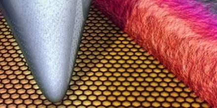
The Illinois team used an atomic force microscope (AFM) tip as a temperature probe to make the first nanometer-scale temperature measurements of a working graphene transistor. The measurements revealed surprising temperature phenomena at the points where the graphene transistor touches the metal connections. They found that thermoelectric cooling effects can be stronger at graphene contacts than resistive heating, lowering the temperature of the transistor.

Click to Enlarge

Image: An atomic force microscope tip scans the surface of a graphene-metal contact to measure temperature with spatial resolution of about 10nm and temperature resolution of about 250 mK.  Color represents temperature data. Alex Jerez, Beckman Institute Imaging Technology Group.

Future computer chips made out of graphene could be faster than silicon chips and operate at lower power, if scientists can grasp a thorough understanding of heat generation and distribution in graphene devices.

The researchers were led by mechanical science and engineering professor William King and electrical and computer engineering professor Eric Pop.

All electronics dissipate heat as a result of the electrons in the current colliding with the device material, a phenomenon called resistive heating. This heating outweighs other smaller thermoelectric effects that can locally cool a device. The speed and size of computer chips are limited by how much heat they dissipate. Computers with silicon chips use fans or flowing water to cool the transistors, a process that consumes much of the energy required to power a device. Graphene’s apparent self-cooling effect means that graphene-based electronics could require little or no cooling.

"In silicon and most materials, the electronic heating is much larger than the self-cooling," King said. "However, we found that in these graphene transistors, there are regions where the thermoelectric cooling can be larger than the resistive heating, which allows these devices to cool themselves. This self-cooling has not previously been seen for graphene devices."

"Our measurements and simulations project that thermoelectric effects will become enhanced as graphene transistor technology and contacts improve," said Pop, who is also affiliated with the Beckman Institute for Advanced Science, and the Micro and Nanotechnology Laboratory at the U. of I.

Next, the researchers plan to use the AFM temperature probe to study heating and cooling in carbon nanotubes (CNTs) and other nanomaterials.

King also is affiliated with the department of materials science and engineering, the Frederick Seitz Materials Research Laboratory, the Beckman Institute, and the Micro and Nanotechnology Laboratory.

The Air Force Office of Scientific Research and the Office of Naval Research supported this work.

The team published its findings in the April 3 online edition of the journal Nature Nanotechnology (http://www.nature.com/nnano/journal/vaop/ncurrent/full/nnano.2011.39.html). Co-authors of the paper included graduate student Kyle Grosse, undergraduate Feifei Lian and postdoctoral researcher Myung-Ho Bae.

Follow Small Times on Twitter.com by clicking www.twitter.com/smalltimes. Or join our Facebook group

April 4, 2011 – BUSINESS WIRE — Thin Film Electronics ASA (Thinfilm) and PARC, a Xerox company, entered the next phase of their co-innovation engagement for printed memory devices. This next phase extends the engagement to prototyping the product for manufacturing readiness.

PARC and Thinfilm’s collaboration on next-generation printed memory solutions kicked off last year with joint design of Thinfilm 128-bit Addressable Memory, which combines Thinfilm’s non-volatile memory (NVM) technology with PARC’s printed CMOS transistor technology.

Thinfilm will use the PARC CMOS technology to expand the memory technology that it has previously commercialized in a roll-to-roll (R2R) printed production process to an addressable version that is still fully printed. Products with Thinfilm addressable memory will be a key avenue for PARC to commercialize its technology.

"Our mutual goal is to reach the printed addressable memory prototype by the end of this year. Key work is already being done at PARC, working closely with Thinfilm’s engineers," said Dr. Ross Bringans, VP of PARC’s Electronic Materials and Devices research. "Thinfilm will utilize PARC background IP for the printed memory application."

"We expect to transfer the contact-based 128-bit memory array to production in 2012. This addressable memory meets the need for creating ubiquitous low-cost tags and disposable printed systems," Davor Sutija, Thinfilm CEO said.

Such memory enables unique form factors, cost advantages, and integration with other printed components including sensors and simple displays that can be customized for multiple markets — ranging from games and toys, to ID tags, disposable sensors, and price labels, notes Ana Arias, co-head of Thinfilm’s Technology Council, U.C. Berkeley Associate Professor in EECS.

To learn more about Thinfilm, please see www.thinfilm.no.

To learn more about PARC, please see: www.parc.com.

Subscribe to Solid State Technology/Advanced Packaging.

Follow Advanced Packaging on Twitter.com by clicking www.twitter.com/advpackaging. Or join our Facebook group

April 1, 2011 — Scientists at the National Institute of Standards and Technology (NIST) have developed a way to measure the wear and degradation of the microscopic probes used to study nanoscale structures in situ and as it’s happening. Their technique can speed up and improve the accuracy of the most precise and delicate nanoscale measurements done with atomic force microscopy (AFM).

Click to Enlarge

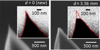
Image. As an atomic force microscope’s tip degrades, the change in tip size and shape affects its resonant frequency. That can be used to accurately measure, in real time, the change in the tip’s shape. Credit: Jason Killgore, NIST

Today, most researchers stop the measurement to "take a picture" of the tip with an electron microscope, a time-consuming method prone to inaccuracies.

NIST materials engineer Jason Killgore has developed a method for measuring in real time the extent to which AFM tips wear down. Killgore measures the resonant frequency of the AFM sensor tip, a natural vibration rate like that of a tuning fork, while the instrument is in use. Because changes to the size and shape of the tip affect its resonant frequency, he is able to measure the size of the AFM’s tip in increments of a tenth of a nanometer, essentially atomic scale resolution. The technique, called contact resonance force microscopy, is described in a paper recently published in the journal Small. (J. P. Killgore, R. H. Geiss and D. C. Hurley. Continuous measurement of AFM tip wear by contact resonance force microscopy. Small. Published March 15, 2011.)

Knowing how fast and to what extent the tip is being worn away during the measurement has been the challenge for researchers and manufacturers trying to create images of the surfaces of nanomaterials and nanostructures. Taking a photo is impossible at such small scales, so researchers use atomic force microscopes to measure peaks and valleys as it’s dragged back and forth across a surface. These devices are used extensively in nanoscale imaging to measure the contours of nanostructures, but the AFM tips are so small that they tend to wear down as they traverse the surface being measured.

Thousands of AFMs are in use at universities, manufacturing plants and research and development facilities around the world. Improving their ability to measure and image nanosized devices will improve the quality and effectiveness of those devices. Another benefit is that developing new measurement tips — and studying the properties of new materials used in those tips — will be much easier and faster, given the immediate feedback about wear rates.

The National Institute of Standards and Technology (NIST) is an agency of the U.S. Commerce Department.

Follow Small Times on Twitter.com by clicking www.twitter.com/smalltimes. Or join our Facebook group

By Debra Vogler, senior technical editor

April 1, 2011 — Daniel Duffy, research scientist in Henkel’s Advanced Technology Group, was a presenter at MEPTEC’s The Heat is On event (3/21/11, Santa Clara, CA). Summarizing the encapsulant materials used for high-brightness LEDs (HB-LEDs), he noted the pros and cons of epoxy and silicone. The material challenges for epoxies are temperature stability and color (aging); and for silicone, contamination and adhesion, as well as barrier properties. In the future, epoxies will have to be stable with respect to blue light (T>150ºC); and silicone material will have to fulfill the condition T<Tg CTE <60ppm/K. "Silicone encapsulants are very stable," said Duffy. "But it is not enough — future power demands require higher levels of photo-thermal stability."

Die attach material challenges include transparency, CTE, interfacial TC, and adhesion properties. Such materials will need to have stable thermal resistance, high TC, matched TCE, and good adhesion properties. Duffy specifically mentioned adhesion as a critical property for LED packaging. "Delamination leads to increased interfacial thermal resistance," said Duffy. "Localized temperature increases can shorten device life." Furthermore, cracking can lead to weakening of wire bonds and cracks; also, delamination weakens barrier protection.

In this podcast interview, Duffy discusses the outlook for new materials and/or enhanced materials for HB-LED applications, including quantum dots. "Quantum dots are very interesting materials…when we learn how to tune the interactions between then and the rest of the materials involved in LED packaging, they will play a continuous role in the future," said Duffy. "They offer a wide variety of colors, tunability of color, and lots of options for tuning their performance with temperature, with time and, maybe even other optical effects we’re not even considering now…they’re here to stay."  The challenge, he noted, will be getting them into materials for higher-power applications.

Listen to Duffy’s podcast interview:  Download (iPhone/iPod users) or Play Now


Subscribe to Solid State Technology/Advanced Packaging.

Follow Advanced Packaging on Twitter.com by clicking www.twitter.com/advpackaging. Or join our Facebook group

Executive Overview

The cleaning process performance in both conventional wet-bath and a single-wafer processor was evaluated. Experiments performed in this study were primarily oriented toward the determination of the number of particles added onto the wafer by using various pumping methods. In particular, the impact of pump-induced particles on silicon wafer cleaning in DI water was investigated. The random yield of ICs was estimated from the particle count data using various correlations including a negative binomial model.

R. Prasanna Venkatesh, Jung-Soo Lim, Jin-Goo Park, Hanyang University, Ansan, Korea

Particle contamination in the microelectronic fabrication process must be below the threshold limit, i.e., <100 each [1], otherwise it would eventually result in yield loss. It is reported in the literature that 75% of total yield loss is coming from particle contamination during manufacturing steps [2], hence this issue has been drawing much attention in recent years. However, to our knowledge, there is no experimental evidence on the effect of pumping methods on particle contamination on the wafer during the cleaning step. Therefore, in this study, the performance of the magnetic levitation centrifugal pump (MLC-BPS 600, Levitronix) during the cleaning operation is evaluated and compared with traditional diaphragm pumps (D1 and D2) in terms of particles added onto the wafer.

Recirculation of DI water was carried out for 24 hours and the recirculated DI water was exposed to 8" bare silicon wafers in both a conventional wet-bath tool, and a single-wafer cleaning processor (Goldfinger, Akrion, USA). Wafers were exposed to the cleaning system at the end of every four hours for the typical process time of 10 minutes and 30 seconds in the conventional wet-bath, and single-wafer processor, respectively. The number of particles on the wafer was measured using a laser surface particle scanner (ST 6600, KLA-Tencor, USA). Experiments were conducted at different flow rates (15 and 10 lpm) for a single pressure of 30psi in a conventional wet bath tool. In the single tool, the flow rate was kept at the maximum value of each pump: 20 lpm for the MLC pump, and 15 lpm for both the D1 and D2 pumps.

Pump-induced particle contamination

The effect of pumping methods on the number of particles added onto the wafer during the 24-hour cleaning test in the wet bath is shown in Fig. 1 (a-c). In the case of the BPS-600 pump, the total number of added particles on the wafer is below 5000 at all the flow rates. In the case of both the D1 and D2 pumps, the particle count on the wafer goes beyond the detection range of the instrument. The maximum measuring capability of the laser surface scanner is 30,000 particles. If the wafer has particles that are beyond the instrument inspection limit, then it could not detect the total number of particles and displays the error message. In that case, the number of particles on the wafer would be more than 30,000. In both of these diaphragm pumps, the total number of added particles on the wafer increases with flow rate as shown in Fig. 1 (b-c). This behavior is more common in pumps as the particle shedding from the pumping system increases with the increase in flow rate [3]. However, in the case of the BPS-600, the opposite behavior is observed, i.e., the number of particles is more for the lower flow rate especially after 12 hours of circulation. The reason for this behavior is not yet clear.

Fig. 1: Particle count on the wafer as a function of circulation time in a wet bath tool for a) MLC pump, b) D1 pump, and c) D2 pump.

The effect of pumping methods on the number of particles added onto the wafer during a 24 hour cleaning test in a single-wafer processor is shown in Fig. 2. In the MLC pump, the total number of particles added onto the wafer is much less (i.e., ~300) and there is no significant change in the number with circulation time. The trend looks similar with the D2 pump, though the number of particles (500) is slightly higher. However, the particle count slightly increases with circulation time especially after 12 hours. In the case of the D1 pump, the wafer particle count is relatively higher (4200 at the 24th hour) and increases linearly with circulation time. The particle number is significantly lower in this test compared to that of the test carried out in the wet bath because of the lower process time.

 Fig. 2: Particle count on the wafer as a function of circulation time in a single wafer processor tool.

From the cleaning studies performed in both conventional wet-bath and single processor, it can be concluded that the number of particles generated by the BPS-600 pump is lower than the number generated by either of the diaphragm pumps. Closer examination of the particle size distribution shows that the number of particles generated by all three pumps is in the range of 0.173-0.326µm, which is in the critical regime that results in yield loss of ICs as reported in the literature [2]. In the following section, the chip yield is calculated using the particle count data.

Chip yield calculation

The addition of particles on the wafer during chemical and DI rinses would be critical to reduce the device yield. The yield loss due to the particle contamination is calculated by correlating the number of particles in ultra pure water (NB)) to the defect density (DO) [4]:

DO = NBSKRPD,

where S is the amount of ultra pure water that contacts the wafer during the fabrication step; KR is the fraction of killing particles, and PD is the probability of particles deposited onto critical areas. For the given process step, the product of SKRPD is constant. Similarly, the other study shows there is a linear correlation between the number of particles in the wet bath (NB) and on the wafer (NW) [5], i.e., NB = ANW.

The value of constant A is also the same for all the pumps if we assume the composition of particles generated by all three tested pumps is the same. Using the above two equations, the ratio of defect density of the two pumps is given by the ratio of the number of particles added onto the wafer.

Then, yield (Y) can be calculated from the defect density using the following negative binomial model [1].

Where Ac is the critical area of the chip and C is a clustering factor. One could estimate the yield variation for different hours of recirculation for different pumps if those values are known. For ready comparison, the chip yield is simulated for all three pumps by assuming the values for DO, MLP =1; C=2 and AC= 0 to 10 cm-2 ; the results are plotted in Fig. 3 and Fig. 4 for both conventional wet-bath and single processor, respectively. The data clearly show that there is a significant difference in the chip yield between the MLC pump and the traditional diaphragm pumps in both cleaning cases.

Fig. 3: Simulated chip yield as a function of critical area for all the three tested pumps. The pump flow rate = 15 lpm; recirculation time = 24hrs.

Fig. 4: Simulated chip yield as a function of critical area for all the three tested pumps. The recirculation time = 24hrs.

Conclusion

The cleaning studies of silicon wafers in DI water in both conventional wet-bath and a single-wafer cleaning tool clearly show that the pumping methods have a strong influence on process performance. Particle contamination on the wafer is lower during pumping with the MLC pump than the traditional diaphragm pumps and consequently, it resulted in a decrease in the yield loss of the ICs. It is therefore critical to choose the right pump for circulating DI water and chemicals during the wafer-cleaning process.

References

1. http://www.itrs.net/Links/2000UpdateFinal/FrontEndProcesses2000final.pdf

2 J.D. Plummer, M.D. Deal, P.B. Griffin. Silicon VLSI Technology – Fundamentals, Practise and Modeling, p. 151, Prentice Hall, New Jersey (2000).

3. M.R. Litchy, R. Schoeb, "Critical Components and Subsystems," Semiconductor Fabtech, 38, 89 (2009).

4. F. Wali, D. M. Knotter, A. Mud, F. G. Kuper, Microelectronic Engineering, 86, 140 (2000).

5. L.W. Shive, K. Ruth, P. Schmidt, Micro: Extreme Silicon part, 1, Feb (1999).

Biographies

R. Prasanna Venkatesh received a bachelors’ degree in chemical engineering from Bharathidasan U., India, and a masters’ degree in petroleum refining and petrochemicals from Anna U., India; he received his PhD in chemical engineering from the Indian Institute of Technology Madras, India and is currently a post-doctoral candidate at Hanyang U., Ansan, 426-791, Korea.

Jung-Soo Lim received his BS in chemical engineering and MS in metallurgy and materials engineering from Hanyang U., Korea, and is a PhD candidate at the university.

Jin-Goo Park received a BS in metallurgy and materials engineering from Hanyang U., Korea, and MS and PhD degrees in materials science and engineering from the U. of Arizona. He is a professor in the Department of Materials Engineering as well as director of the Micro Biochip Center and the Nano-bio Electronic Materials and Processing Lab. (NEMPL), at Hangyang U.; ph.:82-31-400-5226; email [email protected]

More Solid State Technology Current Issue Articles
More Solid State Technology Archives Issue Articles
March 31, 2011 — Sigurd Microelectronics Corporation (Sigurd) will be the first adopter of Multitest’s MT2168 pick-and-place test handler in volume production in Taiwan. The SATS provider will use it to test various QFN packages.

Sigurd, an independent provider of semiconductor assembly and test services (SATS), is known for being a pioneer in employing new IC assembly and test equipment and technologies. Responding to the market requirements, Sigurd continuously improves and upgrades its technology and equipment base.

The recently installed MT2168 ambient-hot pick-and-place handler is used for a hot test application of various small QFN packages. Using the handler in a high-volume environment, Sigurd decided on the fully automated, 16 contact site version of the scalable platform.

After running production tests for several weeks, Sigurd experienced significant advantages from the optimized test cell utilization. Excellent handler jam rate and high soak buffer design allowed the company to almost double daily output.

Sigurd Microelectronics Corporation’s test services cover a wide range of both standard and customized test solutions, including C/P and F/T for logic, analog, mixed-signal, RF, memory and power. The products assembled and tested by the company are extensively used in wireless communication, computing, digital consumer and multimedia products. Sigurd’s customers include many of the world’s leading semiconductor design houses, IDMs and wafer foundries. For more information, visit www.sigurd.com.tw.

Multitest manufactures test equipment for semiconductors, including test handlers, contactors, and ATE printed circuit boards. For more information, visit www.multitest.com.

Subscribe to Solid State Technology/Advanced Packaging.

Follow Advanced Packaging on Twitter.com by clicking www.twitter.com/advpackaging. Or join our Facebook group