Category Archives: Materials and Equipment

March 30, 2011 — Catalysts made of carbon nanotubes (CNT) dipped in a polymer solution equal the energy output and otherwise outperform platinum catalysts in fuel cells, a team of Case Western Reserve University engineers has found.

Liming Dai, professor of chemical engineering and the research team leader, with research associates Shuangyin Wang and Dingshan Yu, found that by simply soaking carbon nanotubes in a water solution of the polymer polydiallyldimethylammoniumn chloride for a couple of hours, the polymer coats the nanotube surface and pulls an electron partially from the carbon, creating a net positive charge.

They placed the nanotubes on the cathode of an alkaline fuel cell. There, the charged material acts as a catalyst for the oxygen-reduction reaction that produces electricity while electrochemically combining hydrogen and oxygen.

In testing, the fuel cell produced as much power as an identical cell using a platinum catalyst. But the activated nanotubes last longer and are more stable, the researchers said.

The simple polymer-coating technique on CNTs can knock down one of the major roadblocks to fuel cell use: cost. Platinum, which represents at least a quarter of the cost of fuel cells, currently sells for about $65,000 per kilogram. These researchers say their activated carbon nanotubes cost about $100 per kilogram.

Unlike platinum, the carbon-based catalyst doesn’t lose catalytic activity or efficiency over time; isn’t fouled by carbon monoxide; and is free from the crossover effect with methanol. Methanol, a liquid fuel that’s easier to store and transport than hydrogen, reduces activity of a platinum catalyst when the fuel crosses over from the anode to the cathode in a fuel cell.

The work is published in the online edition of Journal of the American Chemical Society at http://pubs.acs.org/doi/full/10.1021/ja1112904.

The new process builds on the Dai lab’s earlier work using nitrogen-doped carbon nanotubes as a catalyst. In that process, nitrogen, which was chemically bonded to the carbon, pulled electron partially from the carbon to create a charge. Testing showed the doped tubes tripled the energy output of platinum.

Dai, who is a member of the Great Lakes energy Institute, said the new process is far simpler and cheaper than using nitrogen-doped carbon nanotubes and he’s confident his lab will increase the energy output as well. The researchers believe they can boost the power output and maintain the other advantages by matching the best nanotube layout and type of polymer.

Learn more at http://www.case.edu/.

Also read the Energy Storage Trends Blog

Follow Small Times on Twitter.com by clicking www.twitter.com/smalltimes. Or join our Facebook group

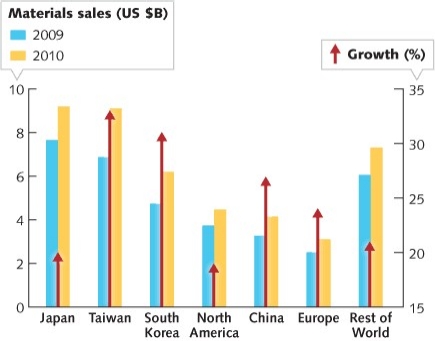
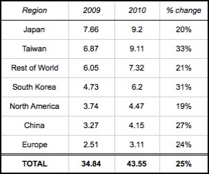
March 29, 2011 – Sales of semiconductor materials rose 25% in 2010 to a new record $43.55B thanks to surging device shipments, according to final tallies from SEMI.

Broken down, wafer fabrication materials tallied $22.93B in 2010, up 29% from 2009 ($17.75B); packaging materials grew slightly slower at ~21% ($20.63B vs. $17.09B). SEMI pointed to particularly "significant increases" in sales of silicon and advanced packaging substrates.

By region, everyone enjoyed double-digit growth. Japan is still the planet’s biggest consumer of semiconductor materials, though Taiwan’s large foundry and packaging provider base consumed 45% more materials (by value) in 2010 to narrow the gap ($9.20B vs. $9.11B). One major growth factor: rocketing gold prices (up around 27% in 2010), particularly helpful for regions with strong packaging bases.

Compared with SEMI’s initial projections at SMC in January, it looks like South Korea and China finished 2010 slightly ahead of expectations (31% vs. 29%. and 27% vs. 25%, respectively), while Japan (20% vs. 22%) came in a couple of percentage points lower.

Click to Enlarge


Click to Enlarge
Semiconductor materials market by region, in US $B and Y/Y growth. Figures may not add due to rounding. "Rest of World" aggregates Singapore, Malaysia, Philippines, other areas of Southeast Asia, and smaller global markets. (Source: SEMI)


By Debra Vogler, senior technical editor

March 29, 2011 — Xradia has unveiled its latest micro computed tomography (CT) 3D X-ray imaging system, the VersaXRM, targeting gaps in the semiconductor, materials science, geomaterials, and life sciences market segments. Kevin Fahey, PhD, VP of marketing at Xradia, told ElectroIQ that the new system is able to provide a large working distance (i.e., the distance between the source spot and rotation axis of the sample) at high resolution (non-destructive).

Click to Enlarge
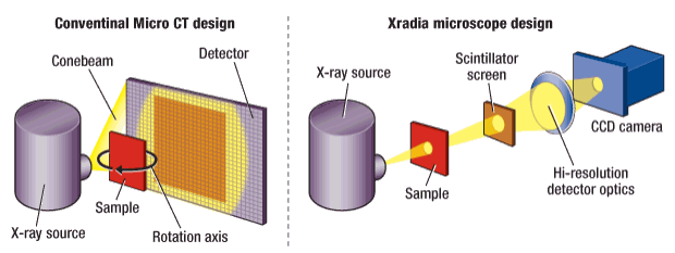
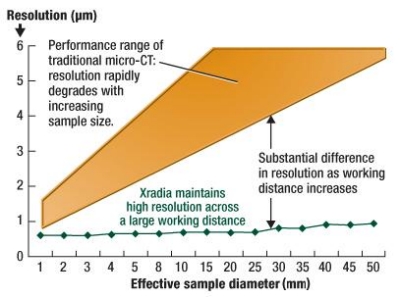
Figure 1. Maintaining resolution across a large working distance. Source: Xradia.

Xradia says that the system can handle a >10× larger sample size for imaging at the same resolution as conventional systems. Large working distances are important to these market segments as they enable in-situ study using environmental chambers or load cells as well as study under varying environmental conditions.

Complex 3D packaging has generated an additional class of defects that come about because of the new solder and dielectric materials, and geometries (e.g., sub-micron voids and cracks). These defects are difficult to detect inside an intact package.

Listen to Fahey’s interview: Download (iPod/iPhone users) or Play Now

In this podcast interview, Fahey discusses how the new platform uses geometrical magnification in tandem with an X-ray microscope. Conventional microCT systems use only geometric magnification technology. By coupling geometrical magnification and optical magnification, "the combination gives very high resolution and allows the sample to sit in an environment where it is not overly sensitive to position away from the source, so we can use larger samples, or larger source-to-sample distances while maintaining high resolution," said Fahey. Modest geometrical magnification (small cone angle) works in tandem with high optical magnification.

Click to Enlarge
Figure 2. Resolution working distance benefits of microscope design. Source: Xradia.

There are many different elements that contribute to resolution: a combination of spot size of the source, the geometry of the system, the resolution of the camera, the scintillator material, vibrations in the system, any thermal variance, and so forth. "Because it’s difficult to test and specify resolution, it’s common place to focus on one of these elements as the dominant factor," noted Fahey. Conventional geometric projection systems tend to be overly sensitive to spot size, called spot blurring (fringes around the sample), explained Fahey. In comparison, the new system is not sensitive to spot size, which means larger spot sizes can be used. In turn, this means larger sources, which are inherently more stable, can be used, improving reliability.  

Click to Enlarge

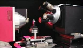
Figure 3. Xradia microscope.

Fahey concludes the interview discussing throughput of a typical 3D IC package failure analysis.

Subscribe to Solid State Technology/Advanced Packaging.

Follow Solid State Technology on Twitter.com via editors Pete Singer, twitter.com/PetesTweetsPW and Debra Vogler, twitter.com/dvogler_PV_semi.

Or join our Facebook group

March 28, 2011 — A Harvard bioengineer and an MIT aeronautical engineer have created a new device that can detect single cancer cells in a blood sample, potentially allowing doctors to quickly determine whether cancer has spread from its original site.

Click to Enlarge

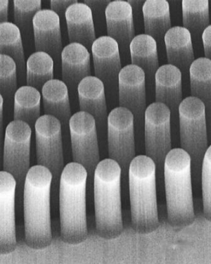
These posts, made of carbon nanotubes, can trap cancer cells and other tiny objects as they flow through a microfluidic device. Each post is 30 microns in diameter. Image: Brian Wardle.

The microfluidic device, described in the March 17 online edition of the journal Small, is about the size of a dime, and could also detect viruses such as HIV. It could eventually be developed into low-cost tests for doctors to use in developing countries where expensive diagnostic equipment is hard to come by, says Mehmet Toner, professor of biomedical engineering at Harvard Medical School and a member of the Harvard-MIT Division of Health Sciences and Technology.

Click to Enlarge

This tiny microfluidic device can separate cancer cells from normal blood cells. Image: Brian Wardle.

Toner built an earlier version of the device four years ago. In that original version, blood taken from a patient flows past tens of thousands of tiny silicon posts coated with antibodies that stick to tumor cells. Any cancer cells that touch the posts become trapped. However, some cells might never encounter the posts at all.

Toner thought if the posts were porous instead of solid, cells could flow right through them, making it more likely they would stick. To achieve that, he enlisted the help of Brian Wardle, an MIT associate professor of aeronautics and astronautics, and an expert in designing nano-engineered advanced composite materials to make stronger aircraft parts.

Out of that collaboration came the new microfluidic device, studded with carbon nanotubes (CNTs), that collects cancer cells eight times better than the original version.

When designing advanced materials, Wardle often uses hollow CNT cylinders whose walls are lattices of carbon atoms. Assemblies of the tubes are highly porous: A forest of carbon nanotubes, which contains 10 billion to 100 billion carbon nanotubes per square centimeter, is less than 1% carbon and 99% air. This leaves plenty of space for fluid to flow through.

The MIT/Harvard team placed various geometries of carbon nanotube forest into the microfluidic device. As in the original device, the surface of each CNT can be coated with antibodies specific to cancer cells. However, because the fluid can go through the forest geometries as well as around them, there is much greater opportunity for the target cells or particles to get caught.

The researchers can customize the device by attaching different antibodies to the nanotubes’ surfaces. Changing the spacing between the nanotube geometric features also allows them to capture different-sized objects: tumor cells (about a micron in diameter), viruses (40nm), etc.

Circulating tumor cells (cancer cells that have broken free from the original tumor) are normally very hard to detect, because there are so few of them — usually only several cells per 1ml sample of blood, which can contain tens of billions of normal blood cells. However, detecting these breakaway cells is an important way to determine whether a cancer has metastasized. "Of all deaths from cancer, 90% are not the result of cancer at the primary site. They’re from tumors that spread from the original site," Wardle says.

Toner’s original cancer-cell-detecting device is now being tested in several hospitals and may be commercially available within the next few years. The researchers are now beginning to work on tailoring the device for HIV diagnosis.

Read the Small abstract and access the article here: http://onlinelibrary.wiley.com/doi/10.1002/smll.201002076/abstract

Courtesy of Anne Trafton, MIT News Office

Follow Small Times on Twitter.com by clicking www.twitter.com/smalltimes. Or join our Facebook group
March 28, 2011 — Henkel Electronics released its Ablestik C100 series conductive die attach films. Available in two formulations — Ablestik C130 and Ablestik C115 supplied in 30 micron and 15 micron thicknesses, respectively — the conductive die attach films eliminate, protect thinner die during attach, and facilite greater bondline control than traditional die attach pastes, says Henkel.

Click to EnlargeAblestik C100 series film die attach materials workability has been established on die sizes ranging from 1 x 1mm up to 6 x 6mm for a variety of package types including both QFNs and QFPs. The materials’ better wetting ability with lower bonding temperature provides stable adhesion strength, allowing robust adhesion against moisture and MSL Level 2 performance on all leadframe surface finishes.

Die attach film provides process control and reliability, especially with thinner wafers, said Kevin Becker, Henkel director of product development for film die attach adhesives, adding that these advantages are now available for conductive as well as nonconductive processes.

Henkel operates worldwide with brands and technologies in three business areas: Laundry & Home Care, Cosmetics/Toiletries, and Adhesive Technologies. For more information on Henkel’s Ablestik C130 or Ablestik C115, visit www.henkel.com/electronics

Subscribe to Solid State Technology/Advanced Packaging.

Follow Advanced Packaging on Twitter.com by clicking www.twitter.com/advpackaging. Or join our Facebook group

Giles Humpston, Tessera Inc.

Modern semiconductors are manufactured with feature sizes measured in nanometers. Despite this, semiconductors are not traditionally classed as nanotechnology. A transistor made with 0.5µm technology does not behave in a manner greatly different to one at the 32nm node. To fit with the modern definition of nanotechnology, materials must exhibit properties that are different from those predicted by simple scaling of dimensions. Their properties are influenced by the laws of physics because the feature size is of the same order as the critical size for physical phenomena. Often the difference is manifest as a step change. For example, the radius of the tip of a crack is typically tens of nanometers. Conventional crack propagation and consequent mechanical failure are impossible if the material dimensions are smaller than this.

Nanotechnology is likely to manifest itself in the semiconductor industry in two forms. The first of these is semiconductor devices themselves. It is well known that we cannot go on shrinking devices ad infinitum. Once the device size approaches single atoms quantum physics comes into play — a transistor may, or may not, switch, depending on the prevailing statistics. Building traditional logic gates out of such devices is not sensible, but other decision-making architectures based on quantum devices are being developed. For solid state memories, an important metric of the material used is the ratio of change between the 1 and 0 states. In a well-designed and fabricated flash memory, the ratio will be around 10,000. By exploiting phase change in the nanomaterial graphene, it is possible to obtain ratios of conductivity over 1 million. If realized in a full-sized memory, this would result in a five-fold increase in storage capacity.

In the near term, the most likely application of nanotechnology to semiconductors is in the area of interconnects. Most recent research effort has been concentrated on carbon nanotubes (CNTs). These materials are ballistic conductors with quantum behavior and exhibit exceptionally low electrical resistance. Values around 10E-4 Ohm-cm have been measured, and they have stable current densities as high as 10E12 A/cm2. One of the major causes of power consumption and propagation delay in semiconductor circuits is the RC time constant of interconnects; reducing R by a factor of 10 will confer significant benefits to conventional semiconductors.

Nanotechnology may even replace the ubiquitous gold plating found on the connectors of virtually every plug-in card. Gold is an excellent conductor, but needs to be a minimum thickness to adequately resist corrosion and add durability. The recent spike in the price of gold is having a measurable effect on connector pricing. Nanomaterials are under development that essentially mimic the electrical and mechanical properties of gold. Because they are base metal alloys, their prices are low and remain stable.

It has been said that the twentieth century was the era of the electron, and the twenty-first century will be the era of the photon. USB3, with its optical interface, is an example of this transition. Nanotechnology, by virtue of its dimensions, is conducive to interacting with light. A well-known example is the quantum dot, one use of which is wavelength conversion. These offer the prospect of designing light-emitting semiconductors with high electro-optic efficiency, and changing the emitted light to the desired spectrum using an engineered coating.

Conclusion

Although there are few examples of commercialized semiconductor nanotechnology, there is no doubt that it offers the prospect of significant innovation by providing materials with properties outside of the current domain. The semiconductor industry, with its large and focused R&D base, is likely to be an early adopter. Research journals abound with papers on nanotechnology, offering a tantalizing glimpse of what the future may hold.

Giles Humpston received his PhD and BSc from Brunel U., U.K. and is director of Research and Development at Tessera, 3025 Orchard Parkway, San Jose, CA 95134 USA; [email protected].

March 24, 2011 – Marketwire — Vendum Batteries (OTCBB: VNDB), a US-based battery technology development company, joined the Nano Knowledge Transfer Network (NanoKTN), a Government agency leading and supporting the commercialization of nanotechnologies in the UK.

NanoKTN is about networking, establishing industry collaborations, partner brokering and accessing R&D and commercialization grant schemes from £5,000 to £250,000 ($7,500 to $390,000). Vendum expects to successfully obtain grants and begin further research and development to further improve its battery technology and immediately commence with pre-production prototypes. Through NanoKTN and working closely with universities, start-up companies like Vendum can build strong supply chains.

Fraser Cottington, CEO of Vendum batteries, believes involvement with NanoKTN is a vital component to linking with the academic community in a meaningful and focused way and allows the company to spread the investment risk, by working with in partnership to achieve common goals, in high-tech battery technology and design.

The NanoKTN aims to simplify the nanotechnology innovation landscape by providing a clear and focused vehicle for the rapid transfer of high-quality information on technologies, markets, funding and partnering opportunities. Objectives include: Improved industrial performance through adoption of nanotechnology; Drive knowledge transfer between companies and the research base; Facilitate interactions through networking and event organization; Provide thought leadership and industry input into UK policy and strategy.

Vendum Batteries has a pending patent on a non-toxic, carbon-based light-weight battery. The paper-thin battery contains none of the toxic elements used in conventional batteries and its carbon nanotube and cellulose-based technology makes it entirely biodegradable. For more information please visit www.vendumbatteries.com

Follow Small Times on Twitter.com by clicking www.twitter.com/smalltimes. Or join our Facebook group
March 23, 2011 — Researchers at Rice University have created a synthetic material that gets stronger from repeated stress, much like the body strengthens bones and muscles after repeated workouts.

Work by the Rice lab of Pulickel Ajayan, professor in mechanical engineering and materials science and of chemistry, shows the potential of stiffening polymer-based nanocomposites with carbon nanotube (CNT) fillers. The team reported its discovery this month in the journal ACS Nano (see the abstract at http://pubs.acs.org/doi/abs/10.1021/nn103104g).

The complex, dynamic interface between nanostructures and polymers in carefully engineered nanocomposite materials enable this self-enhancing quality. Brent Carey, a graduate student in Ajayan’s lab, found the interesting property while testing the high-cycle fatigue properties of a composite he made by infiltrating a forest of vertically aligned, multiwalled nanotubes (MWCNTs) with polydimethylsiloxane (PDMS), an inert, rubbery polymer. Repeatedly loading the material didn’t seem to damage it at all; the stress made it stiffer.

Carey, whose research is sponsored by a NASA fellowship, used dynamic mechanical analysis (DMA) to test their material. He found that after 3.5 million compressions (five per second) over about a week’s time, the stiffness of the composite had increased by 12% and showed the potential for even further improvement.

"It took a bit of tweaking to get the instrument to do this," Carey said. "DMA generally assumes that your material isn’t changing in any permanent way. In the early tests, the software kept telling me, ‘I’ve damaged the sample!’ as the stiffness increased. I also had to trick it with an unsolvable program loop to achieve the high number of cycles."

Materials scientists know that metals can strain-harden during repeated deformation, a result of the creation and jamming of defects — known as dislocations — in their crystalline lattice. Polymers, which are made of long, repeating chains of atoms, don’t behave the same way.

The team is not sure precisely why their synthetic material behaves as it does. "We were able to rule out further cross-linking in the polymer as an explanation," Carey said. "The data shows that there’s very little chemical interaction, if any, between the polymer and the nanotubes, and it seems that this fluid interface is evolving during stressing."

"The use of nanomaterials as a filler increases this interfacial area tremendously for the same amount of filler material added," Ajayan said. "Hence, the resulting interfacial effects are amplified as compared with conventional composites.

Simply compressing the material didn’t change its properties; only dynamic stress — deforming it again and again — made it stiffer.

Carey drew an analogy between their material and bones. "As long as you’re regularly stressing a bone in the body, it will remain strong," he said. "For example, the bones in the racket arm of a tennis player are denser. Essentially, this is an adaptive effect our body uses to withstand the loads applied to it.

"Our material is similar in the sense that a static load on our composite doesn’t cause a change. You have to dynamically stress it in order to improve it."

Cartilage may be a better comparison — and possibly even a future candidate for nanocomposite replacement. "We can envision this response being attractive for developing artificial cartilage that can respond to the forces being applied to it but remains pliable in areas that are not being stressed," Carey said. Read more about nanotech in medical sciences here.

Both researchers noted this is the kind of basic research that asks more questions than it answers. While they can easily measure the material’s bulk properties, it’s an entirely different story to understand how the polymer and nanotubes interact at the nanoscale.

"People have been trying to address the question of how the polymer layer around a nanoparticle behaves," Ajayan said. "It’s a very complicated problem. But fundamentally, it’s important if you’re an engineer of nanocomposites.

"From that perspective, I think this is a beautiful result. It tells us that it’s feasible to engineer interfaces that make the material do unconventional things."

Co-authors of the paper are former Rice postdoctoral researcher Lijie Ci; Prabir Patra, assistant professor of mechanical engineering at the University of Bridgeport; and Glaura Goulart Silva, associate professor at the Federal University of Minas Gerais, Brazil.

Rice University and the NASA Graduate Student Researchers Program funded the research.

Follow Small Times on Twitter.com by clicking www.twitter.com/smalltimes. Or join our Facebook group
March 23, 2011 — There are over 100 production semiconductor fab lines in 53 locations in Japan, say analyst groups IHS iSuppli and Semico. Over a week after the crippling earthquake and tsunami hit northeastern Japan, analysts consider the next business step, with power outages and aftershocks still disrupting production in areas not directly hit by the crisis.

Read more about the earthquake’s impact on microelectronics and photovoltaics industries:

Japan earthquake update: List of facilities impacted

Update: Japan earthquake’s impact on semiconductor community

Electronics in Japan: Earthquake impact from IHS iSuppli

MEMS producers in Japan: Facility updates after earthquake, tsunami

Japan earthquake raises questions of solar supply and replacing nuclear power

Semiconductor facilities in Japan that had suspended manufacturing activities after the earthquake cannot truly commence full production again until the aftershocks cease, notes IHS iSuppli. Earthquakes ranging from 4 to 7 on the Richter scale will make it impossible to fully restart these fabs until the earthquakes stop happening with such frequency, IHS iSuppli research indicates. Every time a quake tops 5, the equipment automatically shuts down.

The IHS iSuppli table lists the locations engaged in volume production for semiconductor manufacturing operations in Japan. It does not include R&D fabs. There are only a few semiconductor manufacturing fabs that sustained substantial damage (Texas Instruments has moved about 60% of its Japan-based production to other facilities, Seiko Epson is moving wafer production as well), says Semico, noting that power outages are more widely disrupting production than actual damage from the earthquake/tsunami. Consistent and reliable electric power supply is still a major issue in Japan’s return to normalcy. Semico believes that high tech and other key industrial facilities, as power hogs, will get high priority.

Letters from semiconductor industry members in Japan:

Live from Japan: Facilities struggling to ramp on power, supply chain disruptions

Letter from Japan: Update on infrastructure, fab status after earthquake 

News from Japan on the impact of disasters

Japan is facing rolling power outages, with frequent electricity supply interruptions in some areas, as several of the country’s nuclear power plants and storage facilities are dangerously damaged. This represents a particular hazard in the production of raw materials for semiconductor manufacturing. Japan’s electrical grid system includes ten utility companies. Semico’s research indicates that extra-high voltage transmission lines link the entire country from Hokkaido in the north to Kyushu in the south. The companies work together to exchange electricity to provide power in the most efficient manner possible in order to cope with emergency situations. These companies also take part in the cooperative development of electric power technology and the sharing of resources. Semico is promoting the use of sand, boric acid, and concrete to encase and seal off the damaged nuclear power facilities, much like Russia’s actions in the Chernobyl disaster.

Japan is the world’s leading producer of the main raw material used in semiconductor manufacturing: silicon. The Japanese earthquake has resulted in the suspension of one-quarter of the global production of silicon wafers used to make semiconductors, reports iSuppli. Manufacturing operations have stopped at Shin-Etsu Chemical Co. Ltd.’s Shirakawa facility. MEMC Electronic Materials Inc. also stopped manufacturing at its Utsunomiya plant. Together, these two facilities account for 25% of the global supply of silicon wafer used to make semiconductors.

Shin-Etsu’s Shirakawa plant is responsible for 20% of global silicon semiconductor wafer supply. The plant is located in Nishigo Village, Fukushima Prefecture Shin-Etsu reported that there has been damage to the plant’s production facilities and equipment. To compensate for the lost manufacturing, Shin-Etsu said it would set up production systems at other facilities. However, the company warned it was unclear how long it would take to restore the damaged facilities and equipment.

MEMC said it evacuated employees and suspended operations at its Utsunomiya plant after the earthquake. The Utsunomiya facility accounts for 5% of worldwide semiconductor wafer supply. MEMC said it expects that shipments from this facility will be delayed during the near term.

The country is also a major provider of chemicals for semiconductor production. Some of these chemicals are hazardous, and power interruptions could lead to dangerous events, such as explosions or the release of poisonous material. In these cases, semiconductor materials facilities facing power interruptions are likely to suspend some operations until a stable power supply can be restored, says IHS iSuppli. Shortages of these materials could cause bottlenecks in the semiconductor production cycle worldwide, adds Semico. Semico believes that in times of shortage companies will find ways to increase efficiencies and improve productivity per wafer. In addition, alternative sources of supply will be found. Also read: Japan earthquake hampering package substrate supplies

In another development for the global electronics supply chain, IHS iSuppli reports that two Japanese companies have stropped production that amounts to 70% of the worldwide supply of the main raw material used to make printed circuit boards (PCBs). The companies, Mitsubishi Gas Chemical Company Inc. and Hitachi Kasei Polymer Co. Ltd., said they will resume production within two weeks of the raw material called copper-clad laminate (CCL).

Many electronic original equipment manufacturers (OEMs) worldwide could be engaging in panic buying of semiconductors and electronic components, spurred by fears of supply disruptions from Japan, says IHS iSuppli. Electronic distributors are reporting a surge in orders from OEM customers, trying to ensure they have sufficient inventory on hand to ride out any interruption in supply.

While the semiconductor supply disruptions are bad, they could have been worse; the recent buildup in global semiconductor inventory may serve to mitigate the impact of reduced supply from Japan. IHS iSuppli in February warned global semiconductor inventory levels had risen to alarmingly high levels, surging to a two–and-a-half year high in the fourth quarter of 2010. Although not completely compensating for supply disruptions from Japan, these excessive inventories may provide some cushion for global semiconductor supply.

While Japan is a major producer of electronic systems, it is a much smaller consumer of such goods, accounting for only about 5.2% of global PC consumption and 5% of worldwide cell phone consumption in 2010, IHS iSuppli research indicates.

Locations of Japan Semiconductor Manufacturing (not including R&D). Source: IHS iSuppli
     
Company Product Technology Location
Elpida Memory Incorporated Memory Hiroshima
Freescale Logic Sendai
Fujitsu Memory, Analog, Discrete Aizu Wakamatsu
Fujitsu Logic Akiruno
Fujitsu Memory, Microcomponent Iwate
Fujitsu Microcomponent, Logic Mie
Matsushita / Panasonic Microcomponent, Logic, Analog, Discrete Arai
Matsushita / Panasonic Discrete Bizen
Matsushita / Panasonic Discrete Hioki
Matsushita / Panasonic Discrete Kyoto
Matsushita / Panasonic Analog, Discrete Nagaokakyoushi
Matsushita / Panasonic Microcomponent, Logic Tonami
Matsushita / Panasonic Logic, Analog Uozu
Matsushita / Panasonic Discrete Utsunomiya
Micron Technologies Optical Nishiwaki
Mitsubishi Analog Kumamoto
Mitsumi Analog Kita-Nihon
ON Semiconductor Logic Aizu
ON Semiconductor Logic, Discrete Gifu
ON Semiconductor Logic, Discrete Gunma
ON Semiconductor Logic, Analog Ojyia
Renesas Electronics Logic Goshogawara, Aomori
Renesas Electronics Memory, Microcomponent, Logic Hitachinaka, Ibaragi
Renesas Electronics Logic, Analog, Discrete Kansai
Renesas Electronics Microcomponents Kita-Nihon
Renesas Electronics Microcomponents Kochi
Renesas Electronics Microcomponent, Logic, Analog, Discrete Koufu
Renesas Electronics Memory, Microcomponent, Logic, Analog Kyuhu
Renesas Electronics Memory, Microcomponent, Logic Saijo
Renesas Electronics Analog, Discrete Takasaki
Renesas Electronics Logic Tsuruoka
Rohm Memory, Analog, Discrete Chikugo
Rohm Logic Hamamatsu
Rohm Memory, Logic, Discrete Kyoto
Rohm Logic, Discrete Miyagi
Rohm Discrete Miyazaki
Rohm Logic Tsukuba
Sieko-Epson Logic, Optical Yasu
Sony Semiconductor Logic, Analog Kyushu Kagoshima
Sony Semiconductor Logic Kyushu Kumamoto
Sony Semiconductor Memory, Microcomponent, Logic Kyushu Nagasaki
Sony Semiconductor Logic Shiraishi
Texas Instruments Analog Hiji
Texas Instruments Analog Inashiki
Toshiba Discrete Hyogo (Himeji)
Toshiba Discrete Ishikawa (Nomi)
Toshiba Discrete Iwate
Toshiba Memory, Analog Mie (Yokkaichi)
Toshiba Logic Nagasaki
Toshiba Logic Oita
     
Phenitec Foundry Ibara, Japan
UMCJ Foundry Tateyama, Japan

Learn more:
Semico
: http://www.mapmodel.com/index.php/2011/03/14/the-impact-of-japans-earthquake-on-the-electronics-and-semiconductor-industries/

IHS iSuppli: http://isuppli.com/Semiconductor-Value-Chain/News/Pages/IHS-iSuppli-Issues-Updates-on-Japan-Earthquake.aspx
http://isuppli.com/Semiconductor-Value-Chain/News/Pages/Japan-Earthquake-Suspends-Supply-of-Raw-Material-Used-in-25-Percent-of-Global-Chip-Production-Memory-Segment-Hit-Hard.aspx

Subscribe to Solid State Technology/Advanced Packaging.

Follow Solid State Technology on Twitter.com via editors Pete Singer, twitter.com/PetesTweetsPW and Debra Vogler, twitter.com/dvogler_PV_semi.

Or join our Facebook group