Category Archives: Materials and Equipment

February 15, 2011 Camtek Ltd. (Nasdaq:CAMT; TASE:CAMT) received an order for multiple wafer inspection systems from one of the world’s largest manufacturers of CMOS image sensors (CIS).

The order includes multiple Falcon systems for 2D inspection. The systems are expected to be installed during the first quarter of 2011.

"Camtek’s inspection systems for CMOS image sensor (CIS) devices…provide a Sub-resolution Detection feature and coverage of a range of CIS process defects, including Color Filter Array (CFA) process control, and thus enable the most reliable detection of critical defects in the image sensor array at a significantly higher throughput," commented Roy Porat, Camtek’s CEO.

The CMOS Image Sensor (CIS) sector is an important market for Camtek’s back-end inspection business. Increasing global demand for camera-embedded hand-held devices, such as mobile phones and tablets, as well as the growing use of cameras in the automotive industry, fuels this sector.

As cameras trend to using CIS with bigger arrays and higher resolutions, more inspection is needed. For example, cameras with 3 megapixels are sample inspected while cameras of 5 megapixels or greater tend to be 100% inspected. "We are expecting additional multiple orders from this strategic customer during 2011," added Mr. Porat.

Camtek Ltd provides automated solutions for semiconductors and Printed Circuit Boards (PCBs) and IC substrates. Learn more at www.camtek.co.il.

Subscribe to Solid State Technology/Advanced Packaging.

Follow Advanced Packaging on Twitter.com by clicking www.twitter.com/advpackaging. Or join our Facebook group

By Debra Vogler, senior technical editor

February 14, 2011 The SOI Industry Consortium recently announced results of an assessment and characterization of fully depleted silicon-on-insulator (FD-SOI) technology (Fig. 1). The study, which was based on the ARM Cortex processor as a prototyping vehicle, concluded that FD-SOI is able to address the increasing low-power, high-performance requirements for mobile and consumer applications. The project was a joint effort among the following consortium members: ARM, Globalfoundries, IBM, STMicroelectronics, Soitec, and CEA-Leti.

Listen to Horacio Mendez’s interview: Download (iPhone/iPod users) or Play Now

Horacio Mendez, executive director of the SOI Industry Consortium, discusses how planar FD-SOI technology enables substantial improvements in performance and power consumption, in a podcast interview with Debra Vogler, senior technical editor. In particular, Mendez describes how it improves on the key metrics for mobile markets: power, frequency, manufacturability, and cost efficiency.

Click to Enlarge

FD-SOI benefits tailored for the mobile market:

  • Simpler technology, straightforward transistor architecture
  • No floating body to worry about
  • Better for SRAM design (lower power, better stability)
  • Better process control, and manufacturability (cost efficient)
Figure 1. FD-SOI transistor. SOURCE: SOI Consortium

Mendez also explains some of the physics behind the inherent stability of FD-SOI devices. In conventional (bulk) devices, implants are used to help control leakage and hit threshold voltage requirements. Because the location of the implants is not precise enough, the device will have random fluctuations that impact these parameters. “Because of the architecture of FD-SOI, implants are not needed to control the device threshold,” said Mendez. “So that gives you a very stable and predictable way to manufacture these devices and in turn.” In turn, he points out that this provides a very good value proposition for the bit cell and further explains the details in the podcast. Early benchmarks on FD-SOI technology demonstrate the ability to reduce the SRAM operating voltage by 100-150mV, thereby reducing memory power consumption up to 40% while maintaining the stability of the SRAM. 

  LP Bulk, 
Generation N
LP Bulk, 
Generation N +1
  FDSOI, 
Generation N +1
VDD Normalized 
frequency to 1
Typical % 
performance
improvement
  Additional % 
performance 
improvement
0.7 1 +25%   +80%
0.8 1 +25%   +40%
0.9 1 +25%   +25%

Figure 2. Comparison of traditional low power manufacturing technology processes from one node to another with the use of FD-SOI. SOURCE: SOI Consortium

Traditionally, low power manufacturing technology processes from one generation node to another yield a performance gain ranging from 20-30%. According to Mendez, the new evaluation indicates that when the same transition also includes FD-SOI technology an additional 80% gain can be achieved beyond the traditional increase (Fig. 2).

Mendez further pointed out that FD-SOI processing is simpler as it eliminates a number of mask layers during transistor-forming processing. Several companies have already announced their readiness to go into high-volume production with substrates (e.g., Soitec, SEH, MEMC).

Subscribe to Solid State Technology/Advanced Packaging.

Follow Solid State Technology on Twitter.com via editors Pete Singer, twitter.com/PetesTweetsPW and Debra Vogler, twitter.com/dvogler_PV_semi.

Or join our Facebook group

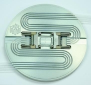
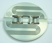
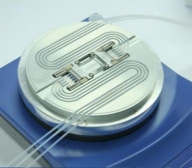
February 14, 2011 — Dolomite, microfluidic designer and manufacturer, expanded its range of temperature control systems with the Hotplate Adaptor – Chip Holder H, which allows control over internal temperatures of microfluidic chips without any disruptions to the fluid flow.

Click to Enlarge Click to Enlarge Click to Enlarge

The use of temperature control systems is vital for many applications including nanostructure generation, controlled microreactions, and droplet microfluidics where droplets can be kept at certain temperature to prevent a solidification reaction until the droplets have left the chip.

Holding a microfluidic chip securely in position, the Hotplate Adaptor enables users to pre-heat or post-heat fluids by using the integrated tube heater. Operating over a temperature range up to 100°C, the adaptor is supplied with a removable lid that can be closed to maintain the chip at constant temperatures, which is important for cell-based analytical studies to maintain cell viability. A glass viewing window (22mm in diameter) facilitates microscopic observations.

Quick and easy to use, the Hotplate Adaptor has been specifically developed for the Chip Interface H, and is compatible with Dolomite’s Linear Connector 4-way, 1.6mm tubing and microfluidic chips that have a footprint of 22.5 x 15mm.

Dolomite is pioneering the use of microfluidic devices for small-scale fluid control and analysis, enabling manufacturers to develop more compact, cost-effective and powerful instruments. By combining specialist glass, quartz and ceramic technologies with knowledge of high performance microfluidics, Dolomite is able to provide solutions for a broad range of application areas including environmental monitoring, clinical diagnostics, food and beverage, nuclear, agriculture, petrochemical, cosmetics, pharmaceuticals and chemicals. Dolomite’s in-house micro-fabrication facilities include clean rooms and precision glass processing facilities. For more information please visit www.dolomite-microfluidics.com

Follow Small Times on Twitter.com by clicking www.twitter.com/smalltimes. Or join our Facebook group

February 13, 2011 — Henkel Corporation entered into a license agreement with Hitachi Chemical Co. Ltd. for the worldwide manufacture and sales of certain dicing die attach film. 

In this agreement, Hitachi Chemical has granted Henkel a worldwide license under the technology described in Hitachi Chemical’s Taiwanese Patent No. 303454, and all related counterpart patents to manufacture and sell dicing die attach film.

Henkel operates worldwide with leading brands and technologies in three business areas: Laundry & Home Care, Cosmetics/Toiletries and Adhesive Technologies. Visit www.henkel.com/electronics for more information.

Hitachi Chemical Co., Ltd. is an innovating global chemical company. Hitachi Chemical operates in two business segments; Functional Materials Segment and Advanced Components and Systems Segment, and offers a diverse range of products.

Subscribe to Solid State Technology/Advanced Packaging.

Follow Advanced Packaging on Twitter.com by clicking www.twitter.com/advpackaging. Or join our Facebook group

February 11, 2011 – Marketwire — Palomar Technologies, precision microelectronics and optoelectronic packaging systems provider, will hold meetings at Stategies in Light to discuss its recent upgrades to high-brightness light emitting diode (HB-LED) assembly.

Strategies in Light will take place February 22-24 in Santa Clara, CA.

Worldwide account manager for Assembly Services, Steve Buerki, will be on site at the Strategies in Light conference at booth #238. Palomar is offering free admission passes to the Strategies in Light exhibitors’ show floor for attendees to speak with Buerki.

Precision Microelectronics Assembly Services (Assembly Services) is the contract assembly division of Palomar Technologies. Assembly Services provides prototyping, test, measurement and production for high accuracy and complex wire and die attach applications. Additional clean room space was recently added in the California-based laboratory, increasing production capacity by 50%. Assembly Services expertise includes development and production for applications such as HB LEDs, RF power modules, military hybrids and laser diode packages.

Palomar Technologies, a former subsidiary of Hughes Aircraft, provides die attach solutions, wire bonding equipment, optoelectronic packaging systems and contract assembly services. For more information, visit www.palomartechnologies.com.

Subscribe to Solid State Technology/Advanced Packaging.

Follow Advanced Packaging on Twitter.com by clicking www.twitter.com/advpackaging. Or join our Facebook group

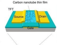
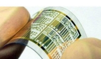
February 10, 2011 — Research teams for Professor Yutaka Ohno Nagoya University (Japan) and Prof. Esko I. Kauppinen, Aalto University (Finland), have developed a simple and rapid technique to fab carbon nanotube (CNT) thin film transistors on plastic film.

Click to Enlarge

The researchers believe they have produced the world’s first carbon nanotubes based on sequential logic integrated circuits (ICs). In the recently developed method, nanotubes are grown using gas phase filtration and thin film transfer to the crucible of plastic on top. This creates a clean and uniform film in a few seconds, researchers report. This method could further be developed into a high-speed roll-to-roll (R2R) manufacturing process.

The inventors believe that the developed carbon nanotube manufacturing process will allow for flexible electronics, such as electronic paper, made at competitive production rates. 

Click to Enlarge

Interest in lightweight and flexible devices, such as a flexible mobile phone and electronic paper, has increased recently. These devices require flexible electronics components, produced cheaply and quickly directly onto plastic substrates.

Carbon nanotubes offer good conductivity and chemical stability, but current CNT manufacturing does not result in CNT transistors with the properties expected. Nanotubes manufactured in the current synthesis process are partially destroyed, whereas the gas phase filtration process leaves them whole, say researchers.

Research results were published in the February 6, 2011 issue of Nature Nanotechnology: http://www.nature.com/nnano/index.html

The study was funded by the New Energy and Industrial Technology Development Organization (Nedo), Japan and the Aalto University Multidisciplinary Institute of Digitalization and Energy Research (MIDE).

For more information, visit http://electronics.tkk.fi/fi/ajankohtaista/uutiset/view/hiilen_nanoputket_valmistettu_muovikalvolle/

Follow Small Times on Twitter.com by clicking www.twitter.com/smalltimes. Or join our Facebook group

February 9, 2011 — Nanocarbon products include single-walled carbon nanotubes (SWCNT or MWNT) and multi-walled carbon nanotubes (MWCNT or MWNT), fullerenes, graphene, carbon nanofiber and nanodiamonds. Carbon nanotubes are microscopic, tube-shaped structures, which essentially have a composition of a graphite sheet rolled into a tube.

Carbon nanotubes have unique, interesting and potentially useful electrical and mechanical properties, and offer potential for various uses in electronic devices. Carbon nanotubes also feature extremely high electrical conductivity, very small diameters (much less than 100nm), large aspect ratios (i.e. length/diameter ratios greater than 1000), and a tip-surface area near the theoretical limit (the smaller the tip-surface area, the more concentrated the electric field, and the greater the field enhancement factor). These features make carbon nanotubes ideal for electron field emitters, white light sources, lithium secondary batteries, hydrogen storage cells, transistors, and cathode ray tubes (CRTs).

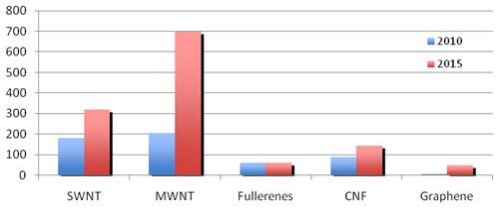
According to a recently published report from iRAP, Inc., ET-113: Production and Application of Carbon Nanotubes, Carbon Nanofibers, Fullerenes, Graphene and Nanodiamonds: A Global Technology Survey and Market Analysis, the production capacity for all products was 4,065 tons in 2010, and is expected to exceed 12,300 tons in 2015. The actual production was less than 25% of the capacity in 2010 and about 50% of the capacity in 2015. Total production value is estimated at about $435 million in 2010 and is expected reach a value of $1.3 billion in 2015.
Click to Enlarge
Share of nanocarbon production value according to types, 2010 and 2015 ($ Millions) Source: iRAP, Inc.

Production capacity far exceeds actual production. Only about 340 tons of carbon nano products were produced in 2008, about 500 tons in 2009 and about 710 tons are expected to have been produced in 2010, which represents about 17% of capacity. However, actual production is expected to reach more than 9300 tons in 2015, representing a growth rate of 67.3% annually and about 80% of production capacity.

Prices for all products are expected to fall by an average of about 12% a year for the next five years. Growth is chiefly driven by multi-walled carbon nanotubes. World production capacity for multi-wall carbon nanotubes exceeded 390 tons in 2008, reached 1,500 tons in 2009, and is estimated to exceed 3,400 tons per year (tpy) by the end of 2010. Production capacity for MWNT is projected to reach 9,400 tons by 2015. 

SWCNTs are the most expensive nano carbon product. They are much more difficult to produce than MWCNTs and are best suited for electronic applications. In 10 to 15 years, SWCNT are expected to replace silicon as the key material in computer chips. 

Despite the quickly growing capacity for CNTs, demand has not yet caught up with capacity.  However, manufacturers have been increasing capacity to be ready to capitalize on that future demand, which is expected to grow rapidly over the next five to ten years. 

For both SWCNTs and MWCNTs, Asia’s production capacity is two to three times higher than that estimated for North America and Europe combined; Japan is the prominent leader in the production of MWCNTs, but China and Korea are rapidly catching up.  Use of CNTs in lithium-ion battery electrodes is the current driving force of ton-scale MWCNT production in Japan.

Nanocarbon production value according to types, through 2015 ($ Millions) Source: iRAP Inc.
  2010 2015 AAGR % 
(2010-2015)
SWNT 180 320 12.2
MWNT  105 700 46.7
Fullerenes 61 60 -0.33
CNF  88 144 10
Graphene  0.75 48 130
Total  435 1,272 24

More details of the report are available from Innovative Research and Products (iRAP), Inc., P.O. Box 16760, Stamford, CT 06905, USA, (203) 569-7909, [email protected] or at http://www.innoresearch.net/reportlist.aspx?cid=7

Follow Small Times on Twitter.com by clicking www.twitter.com/smalltimes. Or join our Facebook group

February 9, 2011 — After a year of beta testing and product analysis, CyberOptics Semiconductor, Inc. has released the WaferSense Airborne Particle Sensor (APS) for wafer processing equipment to the semiconductor market. The sensor identifies particle sources in tools, moving through semiconductor process equipment and automation material handing systems to monitor airborne particles. It reports information in real-time on wafer contamination.

Click to EnlargeThe product has a wafer-like shape compatible with existing automation and wireless communication providing real-time data. APS reduces time locating particle sources, according to the company.

With real-time views of particle conditions, process engineers can address specific trouble spots and be better prepared to pass particle qualifications on the first attempt. The metrology device can also be used to establish a baseline and to ensure operations continue on this baseline as part of preventive maintenance.

The Airborne Particle Sensor uses a fan to pull non-corrosive gas or air through a channel as a laser illuminates the air/gas stream while particles scatter light onto the sensors photodiode. Compatible with front-ends, coater/developer tracks, deposition and etch equipment, the APS has the ability to detect particles as small as 0.1µm. The automation-friendly semiconductor sensor doesn’t require engineers to open chambers or expose ultra-clean process areas to the environment. The sensor can detect particles in real-time without opening the tool.

Using the Airborne Particle Sensor’s companion software, ParticleView and ParticleReview, fab engineers can collect and display particle data wirelessly to see the effect of adjustments in real time.  Particle data can be recorded to compare past to present operations as well as one tool to another to conduct machine-to-machine trend analysis of particle conditions and to establish process control and conduct process improvement.

The Airborne Particle Sensor is available in 200, 300, and 450mm (special order) wafer-like form factors. 

CyberOptics Semiconductor develops wireless products that seamlessly measure critical parameters in semiconductor fabrication processes and equipment. CyberOptics Semiconductor is a subsidiary of CyberOptics Corp. (Nasdaq:CYBE). For more information on the Airborne Particle Sensor, visit http://www.cyberopticssemi.com/products/wafersense/aps/

Subscribe to Solid State Technology/Advanced Packaging.

Follow Solid State Technology on Twitter.com via editors Pete Singer, twitter.com/PetesTweetsPW and Debra Vogler, twitter.com/dvogler_PV_semi.

Or join our Facebook group

February 8, 2011 Carbon nanotubes (CNTs) have many attractive properties, and their structure and areas of application can be compared with those of graphene. To exploit these properties, however, it is necessary to have full control of the manufacturing process. Scientists at the University of Gothenburg successfully defended a thesis on this subject, "In Silco Studies of Carbon Nanotubes and Metal Clusters."

"Our results show that the metal particles that form the basis of the manufacture of carbon nanotubes must have a certain minimum size, in order for growth to start and to continue. It is also probable that the particles are in liquid form at a manufacturing temperature of around 800°C, even though the metals used may have much higher melting points," says Anders Börjesson from the Department of Physics at the University of Gothenburg.

The scientists used various computer models to study in detail properties that are difficult or impossible to examine in experimental conditions. While the diameter of the nanotubes is of the order of one billionth of a metre, and they can be as thin as a single carbon layer, the length of the tubes can extend from the nanometer scale up to several decimeters. Carbon nanotubes can be regarded as thin threads of pure carbon, whose length can be a billion times greater than their thickness.

Click to EnlargeThe thesis In Silco Studies of Carbon Nanotubes and Metal Clusters has been successfully defended. Supervisor: Professor Kim Bolton. The research has been a collaboration between the University of Gothenburg and the University of Borås. Link to the thesis: http://bada.hb.se/handle/2320/6908

For more information on this research, contact Anders Börjesson, Department of Physics, University of Gothenburg, at +46(0)31 786 9143, +46(0)70 240 1145, [email protected]

Courtesy of Anita Fors

Follow Small Times on Twitter.com by clicking www.twitter.com/smalltimes. Or join our Facebook group

February 8, 2011 — The Global School for Advanced Studies (GSAS) invites post-doctorate fellows and other senior student researchers from around the world to apply for the June 20-26 session on "Graphene Fundamentals and Applications" in Grenoble, France.

Selected students, who will receive full travel and lodging support, will compete for fellowships to implement graphene-related research at CEA in Grenoble beginning in January 2012.

Hosted by the GIANT Innovation Campus in Grenoble, this program will create several research teams and challenge them to design a project based on graphene that will leverage their complementary strengths. Each team will have members from around the world and a balance of capabilities, including materials synthesis, characterization, device design and fabrication, theory and measurement.

Teams participating in the Graphene Fundamentals and Applications Session will receive project mentoring from leading global experts. These include Harry Kroto, a Nobel Prize winning professor in the Department of Chemistry and Biochemistry at Florida State University; Sumio Iijima, research fellow at NEC and a professor of materials science at Meijo University in Nagoya who is credited with discovering carbon nanotubes; and Daniel Neumaier, of AMO Research Foundry, and coordinator of the EU’s Graphene-based Nanoelectronic Devices (GRAND), 7th Framework Programme.

Founded in 2006, GSAS is designed to foster innovation in critical global challenge areas such as energy, environment, and health, while training the next generation of young researchers with global leadership capabilities.

The program, which rotates its sessions among campuses and facilities in different countries, groups selected students into interdisciplinary teams that attend lectures, receive expert mentoring and are challenged to develop detailed collaborative research plans in one of the challenge areas. The team whose research plan is chosen receives research fellowships to carry out its projects at GSAS member institutions.

The Graphene Fundamentals and Applications Session is organized by the National Science Fundation (NSF), Northwestern University and CEA-Grenoble (in the frame of GIANT).

Senior graduate students and postdocs from all related disciplines are invited to apply. Visit www.gsasprogram.org for more information.

Follow Small Times on Twitter.com by clicking www.twitter.com/smalltimes. Or join our Facebook group