Category Archives: Mentor Graphics

DENNIS JOSEPH, Mentor, a Siemens Business, Beaverton, OR

As foundries advance their process technology, integrated circuit (IC) layout designers have the ability to deliver more functionality in the same chip area. As more content goes into a layout, the file size also increases. The results? Design companies are now dealing with full-chip Graphic Database System (GDSII/GDS™) layouts that are hundreds of gigabytes, or even terabytes, in size. Although additional storage can be purchased relatively inexpensively, storage availability is becoming an ongoing and increasingly larger concern.

And storage is not the only, or even the most important, issue. File size and layout loading time become increasingly critical concerns as process technology advances. Electronic design automation (EDA) tools can struggle to effectively manage these larger layouts, resulting in longer loading times that can frustrate users and impact aggressive tape-out schedules. Layout loading happens repeatedly throughout the design process—every time designers create or modify a layout, check timing, run simulations, run physical verification, or even just view a layout—so the effect of loading time becomes cumulative throughout the design and verification flow.

Layout designers often try to address the file size problem by zipping their GDS layouts. This approach does reduce file sizes, but it can actually increase loading times, as tools must unzip the file before they can access the data. Need a better, more permanent, solution?

Switch to the Open Artwork System Interchange Standard (OASIS®) format, which can reduce both file sizes and loading times. The OASIS format has been available for almost 15 years [1] and is accepted by every major foundry. It is also supported by all industry standard EDA tools [2].

The OASIS format has several features that help reduce file size compared to the GDS format.

  • OASIS data represents numerical values with variable byte lengths, whereas the GDS format uses fixed byte lengths.
  • OASIS functionality can also recognize complex patterns within a layout and store them as repetitions, rather than as individual instances or geometry objects.
  • The OASIS CBLOCKs feature applies Gzip compression to the individual cells within a layout. Because this compression is internal to the file, tools do not need to create a temporary uncompressed file, which is often necessary with normal Gzip compression. Additionally, although unzipping a Gzip file is typically a single-threaded process, CBLOCKs can be uncompressed in parallel.
  • Strict mode OASIS layouts contain an internal lookup table that can tell a reader the location of different cells within the file. This information allows the reader to more efficiently parallelize the loading of the layout and can offer significant loading time improvement.

Although features such as CBLOCK compression and strict mode are not required, it is highly recommended that layout designers utilize both to realize the fastest loading times in their tools while maintaining small file sizes.

What’s wrong with gds.gz?

Many layout designers have resorted to zipping their GDS layouts, which in measured testcases reduced file sizes by an average of 85%. However, beyond cell placements, designs typically contain a lot of repetition that is not recognized by the GDS format. As a result, much of a GDS file is redundant information, which is why zipping a GDS layout can achieve such significant compression ratios. The OASIS format natively recognizes this repetition and stores this information more compactly. Additionally, taking advantage of CBLOCKs reduced file sizes by an additional 80% from the zipped GDS layouts and by almost 97% from the uncompressed GDS layouts. FIGURE 1 shows the file size reduction that can be achieved by using the OASIS format instead of a zipped GDS layout.

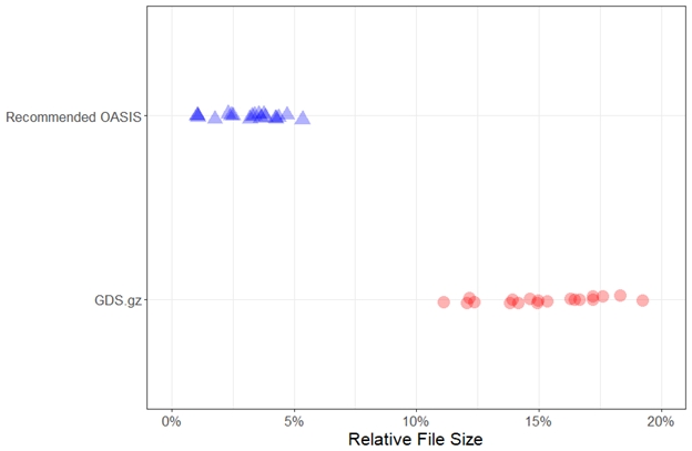
FIGURE 1. File sizes relative to the uncompressed GDS layout (smaller is better). In all measured testcases, the recommended OASIS options delivered smaller file sizes than zipping the uncompressed GDS layout.

In addition, a zipped GDS layout’s file size reductions are usually offset by longer loading times, as tools must first unzip the layout. As seen in FIGURE 2, the DRC tool took, on average, 25% longer to load the zipped GDS layout than the corresponding uncompressed GDS layout. Not only were the corresponding recommended OASIS layouts smaller, the DRC tool was able to load them faster than the uncompressed GDS layouts in all measured testcases, with improvements ranging from 65% to over 90%.

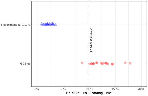
FIGURE 2. DRC loading times relative to the uncompressed GDS layout (smaller is better). In all measured testcases, the recommended OASIS options delivered faster DRC loading times than zipping the uncompressed GDS layout.

While Figs. 1 and 2 considered file sizes and loading times separately, the reality is that layout designers must deal with both together. As seen in FIGURE 3, plotting both quantities on the same chart makes it even clearer that the recommended OASIS options deliver significant benefits in terms of both file size and loading time.

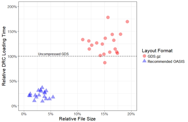
FIGURE 3. DRC loading times versus file size, both relative to the uncompressed GDS layout (smaller is better for both axes). In all measured testcases, the recommended OASIS options delivered faster DRC loading times and smaller file sizes than zipping the uncompressed GDS layout.

Loading time costs are incurred throughout the design process every time a user runs physical verification or even just views a layout. DRC tools are typically run in batch mode, where slow loading performance may not be as readily apparent. However, when viewing a layout, users must actively wait for the layout to load, which can be very frustrating. As seen in FIGURE 4, viewing a zipped GDS layout took up to 30% longer than viewing the uncompressed GDS layout. In addition to the file size reduction of almost 80% (compared to the zipped GDS layout), switching to the OASIS format with the recommended options reduced the loading time in the layout viewer by an average of over 70%.

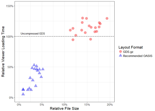
FIGURE 4. Layout viewer loading times versus file size, both relative to the uncompressed GDS layout (smaller is better for both axes). In all measured testcases, the recommended OASIS options also delivered faster loading times than zipping the uncompressed GDS layout.

What about zipping an OASIS layout?

Layout designers may think that zipping an OASIS layout can provide additional file size reductions. However, CBLOCKs and Gzip use similar compression algorithms, so using both compression methods typically provides only minimal file size reductions, while loading times actually increase because tools must uncompress the same file twice.

In a few cases, zipping an uncompressed OASIS layout may reduce file sizes more than using CBLOCKs. However, layout readers cannot load a zipped OASIS layout in parallel without first unzipping the file, which leads to increased loading times. As seen in FIGURE 5, the zipped OASIS layout had 6% smaller file sizes when compared to the recommended OASIS layout. However, DRC loading times increased by an average of over 60% to offset this benefit, and, in several cases, the loading time more than doubled.

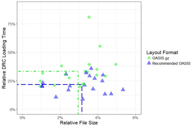
FIGURE 5. DRC loading time versus file size, both relative to the uncompressed GDS layout (smaller is better for both axes), with the means of both axes overlaid. There is a small file size reduction when zipping the uncompressed OASIS layout, but there is a significant loading time penalty.

 What should I do next?

At 16 nm and smaller nodes, block-level and full-chip layouts should be in the OASIS format, specifically with the strict mode and CBLOCKs options enabled. Moving flows to utilize these recommendations can provide dramatically smaller file sizes and faster loading times.

Maintaining data integrity is critical, so layout designers may want to first switch a previous project to the OASIS format to reduce the risk and see firsthand the benefits of switching. They can also run an XOR function to convince themselves that no data is lost by switching to the OASIS format. Additionally, every time physical verification is run on an OASIS layout, it is another check that the layout is correct.

Layout designers can convert their layouts to the OASIS format using industry-standard layout viewers and editors. For best results, designers should enable both CBLOCKs and strict mode when exporting the layout. Designers should also confirm that these features are utilized in their chip assembly flow to reduce the loading time when running full-chip physical verification using their DRC tool.

Conclusion

File size and layout loading time have become increasingly important concerns as process technology advances. While storage is relatively inexpensive, it is an unnecessary and avoidable cost. Longer layout loading times encountered throughout the design process are similarly preventable.

The OASIS format has been around for almost 15 years, is accepted by every major foundry, and is supported by all industry-standard EDA tools. Switching to the OASIS format and utilizing features such as CBLOCKs and strict mode can provide users with dramatically smaller file sizes and faster loading times, with no loss of data integrity.

DENNIS JOSEPH is a Technical Marketing Engineer supporting Calibre Interfaces in the Design-to-Silicon division of Mentor, a Siemens Business. [email protected].

Editor’s Note: This article originally appeared in the October 2018 issue of Solid State Technology. 

Mentor Graphics Corporation today announced an update to the Mentor (R) Embedded Nucleus (R) real time operating system (RTOS) targeting low power, next-generation applications for connected embedded and internet of things (IoT) devices. The Nucleus RTOS supports the development of safe and secure applications utilizing the ARM (R) TrustZone (R) in Cortex (R)-A processors. The ARM TrustZone technology provides a system approach to create processor partitioning that isolates both hardware resources and software to help create a “secure” world that is protected from software attacks.

Non-secure applications are executed in the non-isolated domain – the “normal” world- without the ability to impact the applications executing in the secure world. Devices with safety and security operating requirements can isolate and execute secure applications on the Nucleus RTOS in a trusted environment with priority execution over the non-secure applications in the normal world.  Devices requiring a safe domain with dedicated peripherals for trusted applications to support secure software updates, digital rights management, and trusted payments will benefit from the hardware partitioning technology provided by the ARM TrustZone. This release of the Nucleus RTOS also includes support for low power, resource constrained IoT devices with 6LoWPAN and 802.15.4 wireless connectivity.

The explosive growth of smart IoT connected devices with the proliferation of cloud-based services places new requirements on developers to protect assets from software attacks. The ARM TrustZone enables embedded system developers to allocate system peripherals such as secure memory, crypto blocks, wireless devices, LCD screens, and more to a secure operating domain that is isolated from the remaining system. This hardware separation allows for the development of separate, secure applications on Nucleus RTOS in a trusted environment.

“For IoT and other connected applications, the expanded security and low-power connectivity features in Mentor’s Nucleus RTOS provide many of the capabilities needed for the creation of complex heterogeneous IoT systems,” stated Markus Levy, founder and president of EEMBC and The Multicore Association. “These features complement leading-edge hardware capabilities to meet the needs of today’s advanced IoT embedded systems.”

The applications in the secure world have access to all the system resources while a secure monitor acts to ensure the priority execution over the non-secure normal world applications. The secure monitor provides complete isolation to allow for the execution of bare-metal, Linux (R) or Nucleus RTOS-based applications in the normal world without impacting the safe Nucleus RTOS-based applications in the secure world.  The Nucleus RTOS with ARM TrustZone makes it possible to selectively secure peripherals and applications for system isolation to meet safety and security requirements.

“Nucleus RTOS support for ARM TrustZone provides system developers with the ability to meet the highest levels of safety and security for critical applications for heterogeneous OS-based systems,” states Scot Morrison, general manager of runtime solutions, Mentor Graphic Embedded Systems Division, “ARM TrustZone isolates the general purpose operating system, bare metal or Nucleus RTOS in the normal world from the secure application running in Nucleus RTOS in the secure world.”

IoT wearables, portable medical devices, home automation systems, and other smart connected devices are routinely designed with limited system resources to reduce power consumption and extend battery life. Designed for low data rate IP-driven communication, IPv6 over Lower Power Wireless Personal Area Network (6LoWPAN) is an adaptation layer that can be used to connect resource-limited IoT devices to the internet using IP network links like Ethernet, WiFi, or low power wireless connections. The Nucleus RTOS enables the development of IoT devices with 6LoWPAN to allow the low power exchange of data using TCP, UDP, CoAP transport protocols with compatible application layer security protocols such as DTLS. The use of IPv6 addressing allows every IoT device to have a routable IP address to facilitate internet and cloud access using the standard IP network infrastructure. For low power devices, embedded IoT developers can use 6LoWPAN over 802.15.4 wireless communication. With the Nucleus RTOS, IoT end nodes can be connected, monitored and updated using cloud-based services.

By Ron Press, Mentor Graphics

Three-dimensional (3D) ICs, chips assembled from multiple vertically stacked die, are coming. They offer better performance, reduced power, and improved yield. Yield is typically determined using silicon area as a key factor; the larger the die, the more likely it contains a fabrication defect. One way to improve yield, then, is to segment the large and potentially low-yielding die into multiple smaller die that are individually tested before being placed together in a 3D IC.

But 3D ICs require some modification to current test methodologies. Test for 3D ICs has two goals: improve the pre-packaged test quality, and establish new tests between the stacked die. The basic requirements of a test strategy for 3D ICs are the same as for traditional ICs—portability, flexibility, and thoroughness.  A test strategy that meets these goals is based on a plug-and-play architecture that allows die, stack, and partial stack level tests to use the same test interface, and to retarget die-level tests directly to the die within the 3D stack.

A plug-and-play approach that Mentor Graphics developed uses an IEEE 1149.1 (JTAG) compliant TAP as the interface at every die and IEEE P1687 (IJTAG) networks to define and control test access. The same TAP structure is used on all die, so that when doing wafer test on individual die, even packaged die, the test interface is through the same TAP without any modifications.

When multiple die are stacked in a 3D package, only the TAP on the bottom die is visible as the test interface to the outside world, in particular to the ATE. For test purposes, any die can be used as the bottom die. From outside of the 3D package, for board-level test for example, the 3D package appears to contain only the one TAP from the bottom die.

Each die also uses IJTAG to model the TAP, the test access network, and test instruments contained within the die. IJTAG provides a powerful means for the test strategy to adjust to and adopt future test features. It is based on and integrates the IEEE 1149.1 and IEEE 1500 standards, but expands beyond their individual possibilities.

Our test methodology achieves high-quality testing of individual die through techniques like programmable memory BIST and embedded compression ATPG with logic BIST. The ATPG infrastructure also allows for newer high-quality tests such as timing-aware and cell-aware.

For testing the die IO, the test interface is based on IEEE 1149.1 boundary scan. Bidirectional boundary scan cells are located at every IO to support a contactless test technique which includes an “IO wrap” and a contactless leakage test.  This use of boundary scan logic enables thorough die-level test, partially packaged device test, and interconnect test between packaged dies.

The test methodology for 3D ICs also opens the possibilities of broader adoption of hierarchical test. Traditionally, DFT insertion and pattern generation efforts occurred only after the device design was complete. Hierarchical DFT lets the majority of DFT insertion and ATPG efforts go into individual blocks or die. Patterns for BIST and ATPG are created for an individual die and then retargeted to the larger 3D package. As a result, very little work is necessary at the 3D package-level design. Also, the DFT logic and patterns for any die can be retargeted to any package in which the die is used. Thus, if the die were used in multiple packages then only one DFT insertion and ATPG effort would be necessary, which would then be retargeted to all the platforms where it is used.

Using a common TAP structure on all die and retargeting die patterns to the 3D package are capabilities that exist today. However, there is another important new test requirement for a 3D stack— the ability to test interconnects between stacked dies. I promote a strategy based on the boundary scan bidirectional cells at all logic die IO, including the TSVs. Boundary scan logic provides a standard mechanism to support die-to-die interconnect tests, along with wafer- and die-level contactless wrap and leakage tests.

To test between the logic die and Wide I/O external memory die, the Wide I/O JEDEC boundary scan register at the memory IO is used. The addition of a special JEDEC controller placed in the logic die and controlled by the TAP lets it interface to the memory. Consequently, a boundary scan-based interconnect test is supported between the logic die and external memory. For at-speed interconnect test, IJTAG patterns can be applied to hierarchical wrapper chains in the logic die, resulting in an at-speed test similar to what is used today for hierarchical test between cores.

Finally, for 3D IC test, you need test and diagnosis of the whole 3D package. Use the embedded DFT resources to maximizes commonalities across tests and facilitate pre- and post-stacking comparisons. To validate the assembled 3D IC, you must follow an ordered test suite that starts with the simplest tests first, as basic defects are more likely to occur than complex ones. It then progressively increases in complexity, assuming the previous tests passed.

Industry-wide, 3D test standards such as P1838, test requirements, and the types of external memories that are used are still in flux. This is one reason I emphasized plug-and-play architecture and flexibility. By structuring the test architecture on IJTAG and existing IJTAG tools, you can adapt and adjust the test in response to changing requirements. I believe that test methodologies that develop for testing 3D ICs will lead to an age of more efficient and effective DFT  overall.

Figure 1. The overall architecture of our 3D IC solution. A test is managed through a TAP structure on the bottom die that can enable the TAPs of the next die in the stack and so on. A JEDEC controller is used to support interconnect test of Wide I/O memory dies.

Figure 1. The overall architecture of our 3D IC solution. A test is managed through a TAP structure on the bottom die that can enable the TAPs of the next die in the stack and so on. A JEDEC controller is used to support interconnect test of Wide I/O memory dies.

More from Mentor Graphics:

Model-based hints: GPS for LFD success

Reducing mask write-time – which strategy is best?

The advantage of a hybrid scan test solution

Ron Press is the technical marketing director of the Silicon Test Solutions products at Mentor Graphics. He has published dozens of papers in the field of test, is a member of the International Test Conference (ITC) Steering Committee, and is a Golden Core member of the IEEE Computer Society, and a Senior Member of IEEE. Press has patents on reduced-pin-count testing and glitch-free clock switching.

By Joe Kwan, Mentor Graphics

For several technology nodes now, designers have been required to run lithography-friendly design (LFD) checks prior to tape out and acceptance by the foundry. Due to resolution enhancement technology (RET) limitations at advanced nodes, we are seeing significantly more manufacturing issues [1] [2], even in DRC-clean designs. Regions in a design layout that have poor manufacturability characteristics, even with the application of RET techniques, are called lithographic (litho) hotspots, and they can only be corrected by modifying the layout polygons in the design verification flow.

A litho hotspot fix should satisfy two conditions:

  • First, implementing a fix cannot cause an internal or external DRC violation (i.e., applying a fix should not result in completely removing a polygon, making its width less than the minimum DRC width, merging two polygons, or making the distance between them less than the minimum DRC space).
  • Second, the fix must be LFD-clean, which means it should not only fix the hotspot under consideration, but also make sure that it does not produce new hotspots.

However, layout edges that should be moved to fix a litho hotspot are not necessarily the edges directly touching it. Determining which layout edges to move to fix a litho hotspot can be pretty complicated, because getting from a design layout to a printed contour involves a bunch of complex non-linear steps (such as RET) that alter the original layout shapes, and optical effects that take into account the effect of the layout features context. Since any layout modifications needed to fix litho hotspots must be made by the designer, who is generally not familiar with these post-tapeout processes, it’s pretty obvious that EDA tools need to provide the designer with some help during the fix process.

At Mentor Graphics, we call this help model-based hints (MBH). MBH can evaluate the hotspot, determine what fix options are available, run simulations to determine which fixes also comply with the required conditions, then provide the designer with appropriate fix hints (Figure 1). A fix can include single-edge movements or group-edge movement, and a litho hotspot may have more than one viable fix. Also, post-generation verification can detect any new minimum DRC width or space violations, but it will not be able to detect deleting or merging polygons, so the MBH system must incorporate this knowledge into hint generation. Being able to see all the viable fix options in one hint gives the designer both the information needed to correct the hotspot and the flexibility to implement the fix most suitable to that design.

Figure 1. Litho hotspot analysis with model-based hinting (adapted from “Model Based Hint for Litho Hotspot Fixing Beyond 20nm node,” SPIE 2013)

Figure 1. Litho hotspot analysis with model-based hinting (adapted from “Model Based Hint for Litho Hotspot Fixing Beyond 20nm node,” SPIE 2013)

Another cool thing about MBH systems—they can be expanded to support hints for litho hotspots found in layers manufactured using double or triple patterning, by using the decomposed layers along with the original target layers as an input. This enables designers to continue resolving litho hotspots at 20 nm and below. In fact, we’ve had multiple customers tape out 20 nm chips using litho simulation and MBH on a variety of designs to eliminate litho hotspots

Of course, it goes without saying that any software solutions generating such hints also need to be accurate and fast. But we said it anyway.

As designers must take on more and more responsibility for ensuring designs can be manufactured with increasingly complex production processes, EDA software must evolve to fill the knowledge gap. LFD tools with MBH capability are one example of how EDA systems can be the bridge between design and manufacturing.

Author:

Joe Kwan is the Product Marketing Manager for Calibre LFD and Calibre DFM Services at Mentor Graphics. He previously worked at VLSI Technology, COMPASS Design Automation, and Virtual Silicon. Joe received a BA in Computer Science from the University of California, Berkeley, and an MS in Electrical Engineering from Stanford University. He can be reached at [email protected].

Steffen_SchulzeSteffen Schulze is the director of Marketing, mask Data Preparation and Platform Applications at Mentor Graphics, serving customers in mask and IC manufacturing.

Who knew that mask process correction (MPC) would again become necessary for the manufacturing of deep ultraviolet (DUV) photomasks? MPC can be called a seasoned technology; it has always been an integral part of the e-beam mask writers to cope with the e-beam proximity effects, which can extend up to 15um of the exposure point. In addition, the mask house has been compensating for process-induced biases. Residual errors were always absorbed by the models created to describe the wafer process. Range and general behavior proved to be sufficient to capture the effects and secure the accuracy requirements for the wafer lithography.

At the 40nm node, more complex techniques were considered to cope with significant proximity signatures induced by the dry etch process and the realization that forward scattering in e-beam exposure, which was not accounted for in the machine-based correction, had a significant impact especially in 2D configurations. A number of commercial tools were made available at the time but a broad adoption was thwarted by the introduction of new mask substrates and the associated etch process – OMOG blanks provided for a thinner masking layer and enabled an etch process with a fairly flat signature. The MPC suppliers moved on to the EUV technology domain where a new and thicker substrate with a more complex etch process showed stronger signatures again, along with new effects of different ranges.

So what is changing now? At the 10nm node we are still dependent on the 193nm lithography. And while the wafer resolution is tackled with pitch splitting, the accuracy requirements continue to get tighter – tolerances far below 1nm are required for the wafer model. Phase shift masks are considered with a stack that is higher and displays stronger signatures again. In addition, scatter bars of varying sizes but below 100nm at the mask fall again into the size range with significant linearity effects.

So no wonder that the mask and wafer lithography communities are turning to mask process correction technology again. Wafer models have expanded to a more comprehensive description of the 3D nature of the mask (stack height and width ratio are approaching 1). A recent study presented at SPIE (Sturtevant, et al http://dx.doi.org/10.1117/12.2013748) shows that systematic errors on the mask contribute more than 0.5nm RMS to the error budget.  Figure 1 shows the process biases present in an uncorrected mask for various feature types – dense and isolated lines and spaces. Figure 2 shows how strongly the variability in mask parameters – here stack slope and corner rounding – can influence the model accuracy for a matching wafer model.

Figure 1 copy
Figure 1. Mask CD bias (actual-target) 4X for four different pattern types and both horizontal and vertical orientations. Click to view full screen.
Figure 2 copy
Figure 2 .  Impact of changing the MoSi slope (left) and corner rounding (right) on CTR RMS error at nominal condition and through focus. Click to view full screen.

The authors showed that the proper representation of the mask to a wafer model can improve the modeling accuracy significantly. For example, even an approximation of the corner rounding by a 45deg bevel can have a significant impact. Likewise considering the residual linearity and proximity errors improves the modeling accuracy. Figure 3 shows the comparison of residual errors for a variety of test structure in the uncorrected stage and when simulated with the proper mask model. The latter one can largely compensate the observed errors.

Figure 3
Figure 3. Mask CD error (4X) versus target and residual mask process simulation error. Click to view full screen.

The methods to properly account for the effects during the simulation are anchored in mask processing technology. These results have opened the discussion as to not only describing the mask but also correcting it. The above mentioned study revealed a number of additional parameters that are generally assumed to be stable but fundamentally reveal a high sensitivity of the lithomodel to any variation –specifically the material properties and the edge slope or a substrate over-etch.  From these studies and observations one can conclude that mask process characterization and correction will be of increasing importance for meeting the tolerance requirements for wafer modeling and processing – initially by proper description of its residual errors for consideration in the wafer model but subsequently also by correction. The technology is available for quite some time and ready to be used – unless the materials and the process community come through again.

Read other Mentor Graphics blog posts:

Innovations in computational lithography for 20nm

Looking for an integrated tape-out flow

Gandharv Bhatara is the product marketing manager for OPC technologies at Mentor Graphics.

The long-expected demise of optical lithography for manufacturing ICs has been delayed again, even though the technology itself has reached a plateau with a numerical aperture of 1.35 and an exposure wavelength of 193nm. Immersion lithography is planned for the 20/22nm node, and with the continued delay of EUV, is now the plan of record for 14nm.

How is it possible to use 193nm wavelength light at 14nm? How can we provide the process window to pattern such tight pitches? The secret lies in computational lithography. For 20nm, the two key innovations in computational lithography involve enabling double patterning with concurrent OPC, and in improving difficult-to-print layouts with localized in-situ optimization and by using an inverse lithography technique.

For 14nm, computational lithography offers more tools for process window enhancement with better approaches to sub-resolution assist features (SRAFs). SRAFs have been used since the 130nm node for resolution enhancement, but for 14nm, SRAF placement has evolved considerably. SRAFs placement has traditionally been based on a set of defined rules, which has given excellent coverage for line-space layouts and moderately good coverage for complex 2D layouts, along with fast runtime. However, the final SRAF coverage is highly dependent on the OPC recipe that the user is able to tune. Setting up these highly tuned recipes for 2D layouts can be time consuming, and also inadequate on very complex 2D layouts, leading to catastrophic failures in certain locations. The complexity of developing a well-tuned SRAF rules recipe since the introduction of pixelated sources and the introduction of more sophisticated contact and via layouts has driven lithographers away from rules-based solutions and towards model-based approaches.

Two distinct model-based approaches have developed: inverse lithography (ILT)-assisted and model-based. In the ILT-assisted approach, you use inverse lithography analysis to create a golden reference for a rules-based SRAF placement. ILT provides the ultimate lithography entitlement, but may not be practical to deploy in manufacturing because of increased mask cost and runtime. So, you use ILT only to find the best rules, and then let a rules-based SRAF tool do the actual placement. This gives superior process window for critical blocks like SRAM where the rules are relatively easy to develop.

The second approach is a true model-based approach, where a model is used to determine which areas on mask would benefit most from SRAFS and also to perform the initial SRAF placement. The model-based SRAF optimization reduces dependence on rules generation and improves SRAF placement. Model-based SRAFs can provide a process window that is comparable to that provided by ILT tools, but with much lower mask cost and runtime. The model-based approach is particularly useful for random logic designs, where developing rules continues to be challenging. Figure 1 shows a wafer validation done by IMEC, which shows that the process window obtained using model-based SRAFs and dense OPC was the same as obtained by using an ILT tool.

Given that both the ILT-assisted, rule-based approach and the model-based methods are good, but for different design styles, what if you could combine them easily into a hybrid approach? A hybrid approach combining the best of both solutions provides a single, unified SRAF recipe for SRAM (rules-based) and random logic designs (model-based). This is one of the secrets to 14nm computational lithography: advanced SRAF solutions that provide flexibility, control runtime, and leverage both rules-based and model-based approaches for the most challenging layouts.

Process window with model based SRAFs and ILT
Figure 1. Similar process window with model based SRAFs and ILT


SRAF placement flow high lithography
Figure 2.  A novel hybrid SRAF placement flow guarantees high lithography entitlement and resolves the SRAF development challenge.

DFM Services in the Cloud


February 27, 2013

DFM Services in the CloudJoe Kwan is the Product Marketing Manager for Calibre LFD and DFM Services at Mentor Graphics. He is also responsible for the management of Mentor’s Foundry Programs. He previously worked at VLSI Technology, COMPASS Design Automation, and Virtual Silicon. Joe received a BA in Computer Science from the University of California Berkeley and an MS in Electrical Engineering from Stanford University.

When to Farm Out Your DFM Signoff

The DFM requirements at advanced process nodes pose not only technical challenges to design teams, but also call for new business approaches. At 40nm, 28nm, and 20nm, foundries require designers to perform lithography checking and litho hotspot fixing before tapeout. In the past, DFM signoff has almost always been done in-house. But, particularly for designers who are taping out relatively few devices, the better path may be to hire a qualified external team to perform some or all of your DFM signoff as a service.

 DRC and DFM have changed pretty dramatically over the past few years. At advanced nodes, you need to be more than just “DRC-clean” to guarantee good yield. Even after passing rule-based DRC, designs can still have yield detracting issues that lead to parametric performance variability and even functional failure. At the root of the problem is the distortion of those nice rectilinear shapes on your drawn layout when you print them with photolithographic techniques. Depending on your layout patterns and their nearby structures, the actual geometries on silicon may exhibit pinching (open), bridging (short) or line-end pull-back (see Figure 1).

SEM images of pinching and bridging, 40nm, 28nm and 20nm process nodes
Figure 1: SEM images of pinching and bridging. LPC finds these problems and lets you fix them before tapeout. Litho checking is mandatory at TSMC for 40nm, 28nm and 20nm process nodes.

In the past, these problems were fixed by applying optical proximity correction (OPC) after tapeout, often at the fab. But at 40nm and below, the alterations to the layout must be done in the full design context, i.e. before tapeout, which means that the major foundries now require IC designers to find and fix all Level 1 hotspots. TSMC’s terminology for this is Litho Process Check, LPC.

Usually, design companies purchase the DFM software licenses and run litho checking in-house. This approach has the obvious benefits of software ownership. Designers have full control over when and how frequently they run the checks. The design database doesn’t leave the company’s network. There is a tight loop between updating the design database and re-running verification.

But what if you have not yet set up your own LPC checking flow and need time to plan or budget for software and CPU resources? Or, if you only have a few tapeouts a year? In these cases, you would benefit from the flexibility and convenience of outsourcing the LPC check.

A DFM analysis service is an alternative option to software purchase by performing litho checking for you. Here’s how it works: the design house delivers the encrypted design database to a secure electronic drop box. The analysis service then runs TSMC-certified signoff—for example, Calibre LFD—in a secure data center. Your DFM analysis service should demonstrate that they have an advanced security infrastructure that can isolate and secure you IP. Access should be limited to only those employees that need to handle the data. You would get the litho results back, along with potential guides for fixing the reported hotspots. A cloud-based DFM analysis service for TSMC’s 40nm, 28nm, and 20nm process nodes is available from Mentor Graphics.

A DFM service can also be useful when you already have Calibre LFD licenses, but find yourself with over-utilized computing resources. Having a DFM service option gives you flexibility in getting through a tight CPU resource situation or can ease a critical path in your tape-out schedule. The DMF service can run the LPC while you perform the remaining design and verification tasks in parallel.

Whether you use a DFM services or run LPC in-house on purchased software, it is very important to run litho checking early and often. This lets you identify problematic structures early and allows more time to make the necessary fixes. But now you have more flexibility to make the right business decision regarding how to reach DFM signoff.

Integration is a feature we all look for in our electronic devices. Information readily available on our smart phones is integrated with web-based services and with our personal data on our home computer.  This interoperability that we take for granted is thanks to common software and hardware platforms that are shared by all the elements of this system. Platforms surround us everywhere in our daily lives – the specific model of the car we drive is built on a platform, the electrical systems in our house are on a platform: 110/220V with universal plugs. Platforms?! So I got curious and looked up a more formal definition on Wikipedia:

Platform technology is a term for technology that enables the creation of products and processes that support present or future development.

Why has the concept of platforms been on my mind? Because I hear it more and more often from engineers in the trenches of the post-tapeout flow – people who develop the data preparation sequences that ready their design for manufacturing. They say it is getting increasingly complicated to accommodate all the functional requirements and still meet the TAT (turn-around-time) requirements.  The 20nm node adds additional complexity to this flow – beyond retargeting, etch correction, fill insertion, insertion of assist features and the application of optical proximity correction– now decomposition-induced steps are required and replicate some of the steps for both layers.  Industry standards like the OASIS format enable the communication between independent standalone tools, but are not enough to enable extension in new functional areas and maintain a steady overall runtime performance. Users have to be familiar with all the features and conventions for each tool – not an efficient way to scale up an operation.

The oldest and most versatile platform in computational lithography is Calibre. It started with a powerful geometry processing engine and a hierarchical data base and is accessed through an integrated scripting environment using the Tcl-based  standard verification rule format (SVRF) and the Tcl verification format (TVF). As the requirements for making a design manufacturable with available lithography tools has grown, so has the scope of functionality available to lithographers and recipe developers. APIs have expanded the programming capabilities: the Calibre API provides access to the data base, the lithography API provides access to the simulation engine, the metrology API enables advanced programming of measurement site selection and characterization, the fracture API enables custom fracture (Figure 1). All of these functions let you both build data processing flows that meet manufacturing needs and encode your very own ideas for the most efficient data processing approach. The additional benefit of a unified platform is that it also enables the seamless interaction and integration of tools in a data processing flow. If you can cover the full flow within one platform, rather than transferring giant post-tapeout files between point tools, you will realize a much faster turn-around time.

Common workflow
Figure 1: All tools in the Calibre platform are programmed using the SVRF language and tcl extensions and can be customized via a number of APIs – maintaining a common and integrated workflow.

A platform like Calibre is uniformly used in both the physical verification of the design and in manufacturing, so that innovation entering the verification space flows freely over to the manufacturing side without rework and qualification. Examples include the smart fill applications and the decomposition and compliance checks for double-patterning (DP).

The benefits to using a unified software platform in the post-tapeout flow, illustrated in Figure 2, are also leveraged by the EDA vendor—our software developers use the common software architecture in the platform for very fast and efficient development of new tools and features. This reduces the response time to customer enhancement requests. New technology, like model-based fracture and self-aligned double patterning (SADP) decomposition, were rapidly prototyped based on that.

Calibre workflow
Figure 2: Benefit and scope of a platform solution and the support level provided by Calibre.  


A platform not only provides the integration and efficient operation at the work-flow level, but it also enables efficiency at the data-center level, considering the simultaneous and sequential execution of many different designs and computational tasks. The tapeout manufacturing system is a complex infrastructure of databases, planning, and tracking mechanisms to manage the entire operation. Common interfaces into the tools used –which are guaranteed by a platform solution–let you track data and information associated with each run and manage interactions and feedback across different jobs.  This leads, for example, to an improved utilization of the computer system overall as well as better demand and delivery forecasting. Operating a manufacturing system requires a different level of support than single tool solutions and the necessary infrastructure has evolved with the development of the components.

Once you start using a unified platform in your post-tapeout flow, you will see how the platform expands and grows. For today’s sub-nanometer technologies, a powerful and flexible platform for computational lithography is part of a successful business strategy.

Author biography

Dr. Steffen Schulze is the Product Management Director for the Mentor Graphics’ Calibre Semiconductor Solutions. He can be reached at [email protected].

By Gandharv Bhatara, product marketing manager for OPC technologies, Mentor Graphics.

For nearly three decades, semiconductor density scaling has been supported by optical lithography. The ability of the exposure tools to provide shorter exposure wavelengths or higher numerical apertures have allowed optical lithography to play such an important role over such an extended time frame. However, due to technical and cost limitations, conventional optical lithography has reached a plateau with a numerical aperture of 1.35 and an exposure wavelength of 193nm.  Although intended for the 32nm technology node, it has been pushed into use for the 20nm technology node.

The continued use of 193nm optical lithography at the 20nm technology node brings with it significant lithography challenges – one of the primary challenges being the ability to provide sufficient process window to pattern the extremely tight pitches. Several innovations in computational lithography have been developed in order to squeeze every possible process margin out of the lithography/patterning process.  In this blog, I will talk about two specific advances that are currently in deployment at 20nm.

The first such innovation is in the area of double patterning. As the pitch shrinks to below 80nm, double patterning becomes a necessary processing/patterning technique. One of the impacts of double patterning on the manufacturing flow is that foundries now have to perform optical proximity correction (OPC) on two separate masks after the layout has been decomposed. There are two approaches available to do this. In the first approach, each mask undergoes a separate OPC process, independent of each other. In the second approach—developed, deployed, and recommended by Mentor Graphics—the two masks are corrected simultaneously. This approach allows critical information, like edge placement error and critical dimension, to be dynamically shared across the two masks. This concurrent double patterning approach (Figure 1) ensures the best quality optimal correction, good stitching across the two masks, and significantly reduces the risk of intra-mask bridging.


Caption: Concurrent double patterning OPC corrects the two decomposed masks at the same time, sharing information between them.

The second innovation is in the area of technical advances in OPC techniques. As the process margin gets tighter, traditional or conventional OPC may not be sufficient to process difficult-to-print layouts. These layouts are design rule compliant but require a more sophisticated approach in order to make them manufacturable. We developed two approaches to deal with this situation. The first is to perform a localized in-situ optimization. This is a computationally expensive approach, which precludes it from being a full chip technique that improves printing by enhancing the process margin for extremely difficult-to-print patterns (Figure 2).

Caption: Hotspot improvement with in-situ optimization. The simulated contour lines show an improvement in line width after optimization.

In-situ optimization is integrated within the OPC framework so it’s seamless from an integration standpoint.  The second approach is a technique for post-OPC localized printability enhancement. OPC at 20nm typically uses conventional OPC and simple SRAFs. We developed an inverse lithography technique in which the OPC and the SRAFs have greater degrees of freedom and can employ non-intuitive but manufacturable shapes. This is also a computationally expensive approach, but it allows for significant process window improvement for certain critical patterns and allows for the maximum possible lithography entitlement. In this approach, you first run OPC and identify lithography hotspots (difficult-to-print patterns), then apply the localized printability enhancement techniques on the hotspots. All the necessary tooling and the infrastructure to enable this approach for all major foundries are available.

Both these advances in computational lithography are critical enablers for the 20nm technology node. In my next blog, I will talk about extension of these techniques to the 14nm technology node.

Author biography

Gandharv Bhatara is the product marketing manager for OPC technologies at Mentor Graphics.