Category Archives: OLEDs

April 26, 2011 – BUSINESS WIRE — Universal Display Corporation (NASDAQ: PANL), enabling energy-efficient displays and lighting with its UniversalPHOLED technology and materials, announced advances in the performance of its UniversalP2OLED solution-processible, phosphorescent OLED material systems for use with solution-based manufacturing processes (such as ink-jet printing).

OLED manufacturers are evaluating manufacturing techniques, like ink-jet printing, as additional paths for the cost-effective production of large-area OLED displays and lighting panels. These developments were announced at the International Display Manufacturing Conference (IDMC 2011), held April 18-21, 2011 at the Taipei International Convention Center in Taipei, Taiwan.

Dr. Kwang Ohk Cheon, senior research scientist at Universal Display, reported in a paper titled "Progress in Solution Processible Phosphorescent Organic Light Emitting Devices (P2OLED)" that Universal Display has further enhanced the performance of its UniversalP2OLED red, green and light blue materials systems, as follows:

  • The green P2OLED system, which offers a luminous efficiency of 68 candelas per Ampere (cd/A), has now achieved 175,000 hours of operating lifetime. This represents approximately a 1.3 times improvement in lifetime over results reported last fall.
  • The red P2OLED system, with a luminous efficiency of 18 cd/A, now offers an operating lifetime of 125,000 hours for a two-times improvement in lifetime.
  • The light blue P2OLED system now offers a luminous efficiency of 29 cd/A and 8,000 hours of operating lifetime for a 1.6 times improvement in luminous efficiency and lifetime.
  • Operating voltage reductions were also achieved.

"Commercial viability is now in sight. Solution-based manufacturing techniques could become a cost-effective and attractive option for the production of OLED devices, especially at large sizes," said Steven V. Abramson, president and CEO of Universal Display. Improvements in materials, device design and fabrication techniques drive P2OLED performance closer to the levels currently obtained using vacuum-based manufacturing today. The operating lifetime data is reported as the time to 50% of the initial luminance of 1,000 nits without burn-in.

Small-area OLED displays, manufactured using conventional vacuum thermal evaporation, have already entered the mainstream consumer market in display applications for smartphones and multi-media players. Display and lighting manufacturers are evaluating other techniques for the manufacture of large-area OLEDs in an effort to further drive down costs for OLED TV panel and lighting panel production. Solution-processible techniques, such as ink jet printing, are candidates for the efficient and low-cost manufacturing of large-area OLEDs.

Universal Display Corporation (Nasdaq: PANL) is a leader in developing and delivering state-of-the-art, organic light emitting device (OLED) technologies, materials and services to the display and lighting industries. To learn more about Universal Display, please visit www.universaldisplay.com.

Subscribe to Solid State Technology/Advanced Packaging.

Follow Solid State Technology on Twitter.com via editors Pete Singer, twitter.com/PetesTweetsPW and Debra Vogler, twitter.com/dvogler_PV_semi.

Or join our Facebook group

by Michael A. Fury, Techcet Group

April 26, 2011 – The MRS Spring 2011 meeting is officially open in Moscone West in San Francisco. Fifty-one technical symposia will run concurrently, with over 5000 paid attendees from 50 countries, 3100 oral papers, 1700 posters, 122 exhibitors, and 14,600 entries in the authors’ directory. This author list is comparable to the total MRS membership of ~15,100.

Click to EnlargeThe opening day of this week-long meeting (Monday 4/25) consisted of nine tutorial sessions related to specific symposia topics, and a light load of two technical symposia that were scheduled to get an early jump on the week. Tutorial topics included phase-change materials, NV RAM, compound semiconductors for energy applications, and two sessions related to PV.

A few additional fun facts: running a symposium of this nature requires 38,000 chairs. If we were standing, we probably would not need as much coffee to stay alert — the attendees will consume about 1000 gallons of coffee over five days, for which the MRS will pay the Moscone Center ~$100,000. At $100 per gallon, it is little wonder that the Moscone staff ends the coffee breaks at the appointed time with ruthless efficiency. It also puts the price of gasoline into perspective.


(Additional presentation details can be found online on the MRS Spring 2011 abstracts page. The underscored codes at the beginning of papers reviewed below refer to the symposium, session and paper number.)

OO2.3: Michael Gwinner of the U. of Cambridge presented work on novel light-emitting FETs (LEFETs) which use a 20-30nm thick film of solution processable ZnO or InZnO to lower the electron injection barrier between the Au electrodes and the poly(9,9-dioctylfluorene-alt-benzothiadiazole) (F8BT) channel. This results in an increase in two orders of magnitude in the ambipolar current, and therefore in the light intensity. A blue emitting device was similarly shown with a poly(9,9-dioctylfluorene) (F8) channel.

OO2.4: Jana Zaumseil from U. Erlangen-Nuremberg studied the effect of selectively dispersed single-walled nanotubes (SWNT) in semiconducting polyfluorenes in collaboration with the Cambridge work cited above. Charge injection into the F8BT and F8 was significantly enhanced, even at low concentrations of SWNT. The structures proposed could lead to novel optoelectronic devices operating efficiently in the near-infrared telecommunication wavelength window.

WW2.1: Darrell Schlom of Cornell has apparently found a way around the high point defect levels associated with BaxSr1-xTiO3 films that are formulated for high tunability at microwave frequencies. Such films are desired to exploit the paraelectric-to-ferroelectric transition that occurs just below ambient temperatures. Schlom found that altering layers of SrO and TiO2, with the periodic injection of a double layer of SrO, results in planar defects rather than point defects. Further, biaxial tension induced by lattice mismatch from a judicious choice of substrate results in ferroelectric films. Layering thus provides an additional degree of freedom to tune the ferroelectric properties of materials. This approach is available only to thin films, not to bulk materials. One of his layered compositions, Sr7Ti6O19, has the highest ferroelectric figure of merit of any known material.

OO3.2: Franky So from the U. of Florida fabricated a high-efficiency white OLED device by constructing a blue OLED in a tunable microcavity and capturing the emission with a red-yellow phosphor mix, and further enhancing the efficiency with a macrolens. The net effect is to convert a 68 lm/W blue structure to a 99 lm/W device with excellent white rendering.

OO3.4: N. Erickson of the U. of Minnesota demonstrated a device with a single graded organic layer that transitioned smoothly from 100% hole transmitting material at the anode to near 100% electron transmitting material and the cathode. The resulting external quantum efficiency (16.9%) and power efficiency (61 lm/W) are comparable to figures of merit for more complex multilayer structures. It was proposed that extension of the approach to red and blue emitting devices may provide a path to simple products for white electrophosphorescence.

OO4.1: E.C. Turner of Arizona State has synthesized a series of metal complexes to enhance the phosphorescence of Pt- and Pd-based emitters with Λmax in the range of 420-450nm. These materials exhibit room temperature photoluminescence efficiencies that are several orders of magnitude greater than analogous emitters. The method can be generalized to other phosphorescent complexes for enhancing their emissive properties.

WW2.8: Pankaj Sharma from the U. of Nebraska used piezoresponse force microscopy (PFM) to investigate the 3D arrangement of polarization and switching behavior of ultrathin films of poly(80% vinylidene fluoride-20% trifluoroethylene), or PVDF-TrFE. Switching studies of PVDF-TrFE nanomesas were performed as a function of bias magnitude and duration with sub-10nm spatial resolution.

OO4.6: Hans Spaeth of U. of Cincinnati reported on the operation of biopolymer-based organic light-emitting diodes (BiOLEDs) that incorporate phosphorescent emitting layers. Significant increases in brightness and efficiency have been obtained over fluorescent BiOLEDs. Natural salmon sperm DNA is one of the materials frequently used in research for photonic applications development.


Michael A. Fury, Ph.D, is senior technology analyst at
Techcet Group, LLC, P.O. Box 29, Del Mar, CA 92014; e-mail [email protected].

April 19, 2011 – PRNewswire — TCZ, Cymer Inc. (Nasdaq: CYMI) display equipment product division, received a volume order for the TCZ-1500B, TCZ’s new Gen 5.5 crystallization system, from a leading Asian flat panel display (FPD) manufacturer. This represents TCZ’s second volume order in 2011 and fourth tool customer. The TCZ-1500B system is used for the production of advanced liquid crystal display (LCD) and next-generation organic light-emitting diode (OLED) displays for applications such as high-end smart phones and tablet computers.

Enabled by Cymer light source technology, the TCZ-1500B incorporates a high-power laser for increased throughput, and the Gen 5.5 system allows for a three-time increase in substrate size compared to Gen 4 systems.

Wider adoption of OLED displays has been challenged by the low yield and high costs of OLED technology, and this has limited the number of FPD manufacturers to enter into OLED production. TCZ has developed patented system improvements that use advanced laser beam controls to significantly improve the yield of OLED displays. The increased stability and improved yield of the TCZ-1500B is also expected to reduce the complexity of the manufacturing process, making it easier for new FPD manufacturers to enter the OLED market.

TCZ’s laser crystallization system broadens Cymer’s product offering to meet the display industry need to transition to larger substrate sizes for LCD and OLED displays, said Ed Brown, president and chief operating officer of Cymer.

Cymer Inc. develops light sources used by chipmakers worldwide as the essential light source for DUV lithography systems. Please visit www.cymer.com for additional information.

Subscribe to Solid State Technology/Advanced Packaging.

Follow Solid State Technology on Twitter.com via editors Pete Singer, twitter.com/PetesTweetsPW and Debra Vogler, twitter.com/dvogler_PV_semi.

Or join our Facebook group

April 7, 2011 – BUSINESS WIRE — CCID Consulting Co. Ltd. (HKSE: 08235), China-based ICT research and management consulting firm, released its 2010-2011 Survey on China’s OLED Industry Development at Consumer Electronics Market China 2011 this March in Suzhou.

OLED technology

The CCID survey indicates that the small-sized organic light emitting diode (OLED) technology has become mature and is entering the mobile phone market in a fast manner. OLED featuring self-luminosity, ultra thinness, fast response, wide viewing angle and low power consumption has helped the OLED-screen mobile phones gain great popularity. OLED has initially established its position as the core of the third-generation display. With technical advancement and breakthroughs in the mass production of large-sized OLED, the industry will embrace a new era of larger-sized OLED. Industry analyst firm NanoMarkets released "OLED Lighting Markets Asia-2011," which says the market opportunities in Asia for OLED lighting will generate $2.1 billion by 2016.

iPhone played a significant role in driving the popularity of large-sized smart phones and enabled the debut of OLED screens in the market. The active OLED (AMOLED), in particular, is heavily dependent on high-end mobile phones and larger-sized application consumption. The sales revenue of AMOLED has continued to grow since it beat PMOLED in 2009.

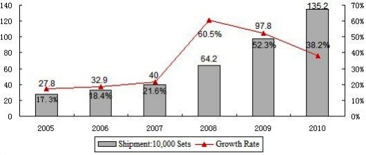
The market has been expanding with the technical advancement and application upgrades. According to CCID Consulting statistics, supported by demand for mobile phones and application products including MP3/MP4, OLED display screen market has been seeing a rapid growth since 2005. In 2010, China’s OLED shipment reached 1.352 million sets, up 38.2% year-on-year, which was attributable to both the growing market demand and the increase in the manufacturers’ capacities.

Currently, most of the OLED panel manufacturers are located in Japan, South Korea and Taiwan. NanoMarkets’ report states that Japan will dominate the OLED lighting business through 2014 despite lingering issues from the earthquake and tsunami. Japanese consumers have greeted LED lighting enthusiastically and will do the same as OLED lighting gets onto retail shelves. Meanwhile, Japanese firms are taking up key positions in every part of the worldwide OLED lighting supply chain from design and manufacture through to wholesale distribution. Sales of OLED lighting in Japan are expected to reach $1.1 billion by 2016.

Korea is early in its embrace of OLED lighting and NanoMarkets predicts sales of only reach $230 million by 2016. But, the influence of both Samsung and LG cannot be understated as both have made a strong commitment to OLED lighting and NanoMarkets notes how Samsung’s strong international brand has brought OLED displays into the mainstream. The firm sees great potential for OLED lighting from Samsung’s involvement in the technology.

With the launches of Samsung SDI’s world’s first AMOLED panel, Sony 11" AMOLED TV and LG’s 15"AMOLED TV, the manufacturers in Japan, South Korea and Taiwan have strengthened their competitiveness in OLED market and also gained a favorable position in the AMOLED market, says CCID. Besides, other manufacturers including LG Display, CMEL, TMD and Samsung Electronics have also accelerated their AMOLED technology development.

Based on its long-term research on the status and development trends of the OLED industry, CCID Consulting forecasts that in the three years to come, the demand for OLED panels will see a rapid growth as the demand for consumer electronics continues to expand.
Click to Enlarge

Figure. Shipment and growth rate of China’s OLED industry, 2005-2010 Source: CCID Consulting, February 2011

China

With the support of China’s Ministry of Industry and Information Technology (MIIT), OLED R&D in mainland China has achieved a number of breakthroughs. In October 2008, Visionox, established by Tsinghua University, completed the first OLED mass production line in Kunshan City of eastern China’s Jiangsu Province, and started the mass production of small-sized OLED display screens.

At the end of 2010, small-sized OLED manufacturers in mainland China included Visionox, Shanwei Truly, Sichuan CCO and IRICO. China’s first AMOLED medium experimental line has been commissioned in Kunshan, which acquired all the required production techniques at the end of 2010. Shanghai Tianma and IRICO, respectively, are in process of constructing G4.5 AMOLED production lines, with debut of mass production expected within 2011, while BOE and Sichuan CCO are also actively engaged in AMOLED R&D projects.

OLED requires planning to integrate resources, facilitate innovations, direct various enterprises to enter the OLED industry chain and grant financial support to achieve sustainable development of the industry in China. Although the addressable market for OLED lighting in China is limited, NanoMarkets expects the Chinese OLED lighting market to reach $420 million by 2016. OLED lighting markets and manufacturing in China are expected to benefit from current Chinese industrial policy which emphasizes the need to develop high-tech industries to serve the domestic Chinese market.

Governmental support continued in 2010 on the basis of the Planning on Adjusting and Revitalizing the Electronic Information Industry issued in 2009, including the MIIT’s special funds for the electronic information industry and industrial demonstration bases, as well as Ministry of Finance’s tax policies on new display manufacturers’ imported materials.

So far, China has not yet formed its OLED industry chain, without any domestic full-set OLED manufacturing equipment producers and with key equipment and full-set equipment technologies dominated by the Japanese, South Korean and European enterprises. It lacks raw materials including indium tin oxide (ITO) glass, photoresist, desiccant and UV curing adhesives for packaging. Meanwhile, China’s development of AMOLED techniques is facing great difficulty due to the backward TFT technologies, inferior panel techniques and inadequate management.

Other weak points of China’s OLED industry include: limited financing channels due to the immaturity of China’s capital market; inadequate basic research, industry standards, and resouces integration; and development and management talents are badly needed.

As China did not enter the CRT and LCD arena at the early stage and failed to develop its core technologies and competitiveness, the country could only join the industry’s low-profit assembling and testing sections with its advantages of cheap labor force and strong OEM capacities. However, the emergence of OLED provides a great opportunity for China’s display industry.

China is both a major producer of the world’s consumer electronics and it is the world’s largest OLED application market. In this market, more than 45% of the IT products are related with display devices; the output of mobile phones in mainland China accounts for over 50% of the global total; the output of MP3/MP4 in mainland China accounts for over 90% of the global output; and the output of other consumer electronics in mainland China accounts for over 50% of the global total. As the cost further goes down and the capacity continues to grow, the OLED panels will be more widely used in other consumer electronics. For instance, the domestic brand Lenovo’s LePhone has adopted a AMOLED screen, marking the debut of OLED on domestic mobile phones.

Driver ICs

Many companies are engaged in the design and production of OLED driver ICs worldwide. The OLED active driver panel has limitations such as high prices and poor compatibility with silicon materials and organic materials, which has become a bottleneck slowing the development of the global OLED industry. China depends on driver IC imports and lags behind other countries in large-sized and color screen technologies due to its outdated equipment and limited investment. In addition, the industry’s key patents are all held by foreign companies. For example, Kodak and Idemitsu Kosan hold the fundamental patents of small molecule OLED materials and structures; CDT and DuPont hold the fundamental patents of polymer PLED materials and structures; SANYO, Sharp, SEL and Eldis, South Korean Samsung, LG and Industrial Technology Research Institute hold certain core patents of active drivers.

CCID Consulting Co. Ltd. is a Chinese consulting firm directly affiliated to China Center for Information Industry Development (CCID Group). Learn more at
http://en.ccidconsulting.com

NanoMarkets tracks and analyzes emerging market opportunities in energy and electronics markets created by developments in advanced materials. Visit www.nanomarkets.net  

Subscribe to Solid State Technology/Advanced Packaging.

Follow Solid State Technology on Twitter.com via editors Pete Singer, twitter.com/PetesTweetsPW and Debra Vogler, twitter.com/dvogler_PV_semi.

Or join our Facebook group

April 1, 2011 – Marketwire — With escalating demand for larger fabs of Gen 8, Gen 8.5 and Gen 10, the liquid crystal display (LCD) and organic light emitting diode (OLED) manufacturing equipment market has witnessed a growth spur. The market will continue its upward growth trajectory through 2011, says analyst firm Frost & Sullivan.

The majority of demand stems from the Gen 8 and Gen 8.5 segment. Burgeoning sales of LCD TVs, smartphones, and advertising screens is triggering high uptake of LCD manufacturing equipment.

During 2010, TFT-CD fab expansions boosted LCD equipment adoption. The intensifying focus on energy efficiency and the gravitation toward environment-friendly products will accelerate demand for OLED displays over the next 3-5 years.

New analysis from Frost & Sullivan, LCD and OLED Manufacturing Equipment Market, finds that the market earned revenues of $7300.3 million and $136.7 million respectively in 2009 and estimates this to reach $18,182.5 million and $702.7 million in 2017.

"The tangible advantages of OLED technology, such as sharper images and better contrast ratios, crisp colors and faster refresh rates compared to any existing display technology will be a key driver," says Frost & Sullivan research analyst Lavanya Rammohan. "OLED also offers consumers better energy management, as the whole system functions at optimal power and is of organic substrate."

As the benefits of OLED displays become more prominent, the demand for OLED manufacturing equipment will witness a hike in the next 3-7 years. Technology innovations, better functionality, and falling prices are expected to keep up the tempo of demand for OLED displays in mobile phones. The market also expects to benefit from increasing demand for OLED displays used for signage.

Deposition and patterning of large substrates remain major impediments for LCD and OLED manufacturing equipment providers. The use of large substrates complicates the deposition process and incurs high capital costs in terms of material deposition and relevant technical issues with throughput and uniform deposition.

Greater emphasis on design and prototyping will continue to revolutionize the display manufacturing equipment markets. As the consumer industry continues to witness increasing panel sizes, deposition with high accuracy and throughput (without affecting integrity of material in the OLED market) will be a key challenge.

"LCD and OLED equipment manufacturers are constantly improving design and functionality of equipment to help overcome deposition challenges and battle bottlenecks," says Rammohan. "They are venturing into open collaboration with customers and creating product roadmaps that enable scalability for future generations of display manufacturing."

Innovative deposition techniques, testing and other processes are expected to spike customer interest and elevate purchasing levels. Going forward, there will be increased collaboration between material providers, display manufacturers, equipment providers and technology enablers to optimize material performance and lifetime. Constant manufacturing process improvement will be imperative to balance the relentless price pressures that confront display manufacturers.

LCD and OLED Manufacturing Equipment Market is part of the Surface Mount Technologies Growth Partnership Service program. All research services included in subscriptions provide detailed market opportunities and industry trends that have been evaluated following extensive interviews with market participants.

If you are interested in a virtual brochure for this study, e-mail Sarah Saatzer, Corporate Communications, at [email protected], with your full name, company name, job title, telephone number, company e-mail address, company website, city, state and country, or visit http://www.frost.com.

Subscribe to Solid State Technology/Advanced Packaging.

Follow Solid State Technology on Twitter.com via editors Pete Singer, twitter.com/PetesTweetsPW and Debra Vogler, twitter.com/dvogler_PV_semi.

Or join our Facebook group

February 3, 2011 — The New Hampshire Innovation Commercialization Center (NH-ICC) has attracted a $100,000 grant from the New Hampshire Innovation Research Center (NHIRC) to help commercialize semiconductor technology developed by Durham, NH-based startup Innovacene. Innovacene was founded last year by University of New Hampshire (UNH) professor Glen Miller to commercialize the semiconductor technology he and his research team developed at UNH’s Center for High-rate Nanomanufacturing in Durham. The company has created an extremely thin, organic, ultra-lightweight surface-emitting semiconductor coating for use in organic light-emitting diodes (OLEDs), according to a press release sent to Mass High Tech.

OLEDs are currently used in light-emitting screens for devices such as mobile phones and computers. Innovacene’s technology would allow manufacturers to apply the coating to large surfaces, such as wallpapers and ceiling tiles, to create a more natural style of lighting.

According to Miller, the company will use the grant funding to develop these ultra-high efficiency lighting products, which will be inexpensive to install and able to be manufactured at high rates.

"These products will produce the highest quality natural white light while consuming a fraction of the energy associated with conventional white lighting products," said Miller.

The company has partnered with the NH-ICC to develop a comprehensive business plan while developing prototype devices, Miller said . They will also be working to identify financing options so that Innovacene can grow quickly to meet the needs of the emerging OLED lighting market.

Mark Galvin, NH-ICC manager director, said the NH-ICC helped with Innovacene’s grant request because of the unique differentiations in the company’s early prototypes. With the correct resources over the next year or so, said Galvin, those differences should allow successful commercialization of Innovacene’s OLED technology. Galvin said he hopes that Innovacene will eventually become a resident of the NH-ICC.

Located at the Pease Tradeport in Portsmouth, the NH-ICC was launched last year by Galvin, a veteran in the telecom industry who founded Cedar Point Communications in Derry, N.H. and Whaleback Systems Corp. in Portsmouth, N.H. 

Learn more about MassHighTech’s story at www.masshightech.com/stories/2011/01/24/daily39-UNH-startup-Innovacene-receives-100K-grant-with-help-from-NH-ICC.html 

Follow Solid State Technology on Twitter.com via editors Pete Singer, twitter.com/PetesTweetsPW and Debra Vogler, twitter.com/dvogler_PV_semi. Or join our Facebook group

(August 17, 2010) — In a podcast interview, Paul Semenza, SVP of Analyst Services at DisplaySearch, explains how a maturing OLED manufacturing capability is contributing to the surge in interest, as is consumer response to products that use OLEDs. One challenge, however, is scaling up vapor deposition, and solutions are being developed. 

Still, he stresses, LCDs aren’t going away anytime soon, and discusses the “battle” between OLEDs and LCDs. The accompanying graph, courtesy of DisplaySearch, indicates continued rapid growth.

OLED revenues in Q1’10 were US$231 million, up 59% Y/Y, and Q2’10 revenues are expected to continue rapid growth. Mobile phones account for 80% of OLED revenues, with the mix moving from small, secondary displays for flip phones to large, main displays for smartphones, enabled by active matrix OLED.


  Q109 Q209 Q309 Q409 Q110 Q210
Revenue ($) 145,242 192,310 245,070 243,942 231,204 276,615
Q/Q growth (%) -7 32 27 0 -5 20
Y/Y growth (%) -13 22 84 57 59 44

Listen to the podcast:

Play Now or Download

Read more about LEDS

Return to the Semiconductors center, or go straight to articles on Wafer Processing

June 9, 2009: For car designers, secret agents in the movies and jet fighter pilots, data eyeglasses — also called head-mounted displays (HMDs) — are everyday objects. They transport the wearer into virtual worlds or provide the user with data from the real environment. At present these devices can only display information.

“We want to make the eyeglasses bidirectional and interactive so that new areas of application can be opened up,” Michael Scholles, business unit manager at the Fraunhofer Institute for Photonic Microsystems IPMS in Dresden.

A group of scientists at IPMS is working on a device which incorporates eye tracking — users can influence the content presented by moving their eyes or fixing on certain points in the image. Without having to use any other devices to enter instructions, the wearer can display new content, scroll through the menu or shift picture elements.

Scholles believes that the bidirectional data eyeglasses will yield advantages wherever people need to consult additional information but do not have their hands free to operate a keyboard or mouse.


Data eyeglasses display information and respond to commands. (Source: Fraunhofer IPMS)

The Dresden-based researchers have integrated their system’s eye tracker and image reproduction on a CMOS chip. This makes the HMDs small, light, easy to manufacture and inexpensive.

The chip, measuring 19.3mm × 17mm, is fitted on the prototype eyeglasses behind the hinge on the temple. From the temple the image on the microdisplay is projected onto the retina of the user so that it appears to be viewed from a distance of about one meter.

The image has to outshine the ambient light to ensure that it can be seen clearly against changing and highly contrasting backgrounds. For this reason the research scientists use OLEDs, organic light-emitting diodes, to produce microdisplays of particularly high luminance.

In industry and in the medical field, the interactive data eyeglasses could enable numerous tasks to be performed more simply, efficiently and precisely. Many scenarios are possible, including patients’ vital functions, MRT and x-ray images for the operating surgeon, construction drawings for erection engineers and installation instructions for service technicians.

Some users have already tried out conventional HMDs, but the results were not very impressive. In most cases they were found to be too expensive, too heavy, too bulky and not very ergonomic.

“We have now overcome these hurdles,” says Scholles. With his team and colleagues from other Fraunhofer institutes he is already working on the next development stage of the bidirectional eyeglasses.

May 22, 2009: China-based panel maker Irico Group Electronics plans to invest $74.38 million in its first OLED production fab, which broke ground in Foshan, China on May 12, 2009, according to a report in Digitimes Displays.

Organic light emitting diodes (OLEDs) are screens based on nanostructured polymer films.

Digitimes cited China media reports as saying that construction of the OLED production fab will take about 16 months, with annual capacity to reach 12 million panels.

The reports noted that Irico also plans to build module and low-temperature polysilicon (LTPS) production lines, according to Digitimes.

May 11, 2009: For more than a decade, scientists have been frustrated in their attempts to create continuously emitting light sources from individual molecules because of an optical quirk called “blinking,” but now scientists at the University of Rochester have uncovered the basic physics behind the phenomenon, and along with researchers at the Eastman Kodak Co., created a nanocrystal that constantly emits light.

The findings, detailed online in Nature, may open the door to dramatically less expensive and more versatile lasers, brighter LED lighting, and biological markers that track how a drug interact with a cell at a level never before possible.

Many molecules, as well as crystals just a billionth of a meter in size, can absorb or radiate photons. But they also experience random periods when they absorb a photon, but instead of the photon radiating away, its energy is transformed into heat. These “dark” periods alternate with periods when the molecule can radiate normally, leading to the appearance of them turning on and off, or blinking.

“A nanocrystal that has just absorbed the energy from a photon has two choices to rid itself of the excess energy — emission of light or of heat,” says Todd Krauss, professor of chemistry at the University of Rochester and lead author on the study. “If the nanocrystal emits that energy as heat, you’ve essentially lost that energy.”

Krauss worked with engineers at Kodak and researchers at the Naval Research Laboratory and Cornell University to discover the new, non-blinking nanocrystals.

Krauss, an expert in nanocrystals, and Keith Kahen, senior principal scientist of Kodak and an expert in optoelectronic materials and devices, were exploring new types of low-cost lighting similar to organic light-emitting diodes, but which might not suffer from the short lifespans and manufacturing challenges inherent in these diodes. Kahen, with help from Megan Hahn, a postdoctoral fellow in Krauss’ laboratory, synthesized nanocrystals of various compositions.


Rendition of the new nonblinking nanocrystal. (Credit: Todd Krauss, University of Rochester)

Xiaoyong Wang, another postdoctoral fellow in Krauss laboratory, inspected one of these new nanocrystals and saw no evidence of the expected blinking phenomenon. Remarkably, even after four hours of monitoring, the new nanocrystal showed no sign of a single blink — unheard of when blinks usually happen on a scale of miliseconds to minutes.

After a lengthy investigation, Krauss and Alexander Efros from the Naval Research Laboratory concluded that the reason the blinking didn’t occur was due to the unusual structure of the nanocrystal. Normally, nanocrystals have a core of one semiconductor material wrapped in a protective shell of another, with a sharp boundary dividing the two. The new nanocrystal, however, has a continuous gradient from a core of cadmium and selenium to a shell of zinc and selenium. That gradient squelches the processes that prevent photons from radiating, and the result is a stream of emitted photons as steady as the stream of absorbed photons.

With blink-free nanocrystals, Krauss believes lasers and lighting could be incredibly cheap and easy to fabricate. Currently, different color laser light is created using different materials and processes, but with the new nanocrystals a single fabrication process can create any color laser. To alter the light color, an engineer needs only to alter the size of the nanocrystal, which Krauss says is a relatively simple task.

The same is true of what could one day be OLED’s successor, says Krauss. Essentially, “painting” a grid of differently sized nanocrystals onto a flat surface could create computer displays as thin as paper, or a wall that lights a room in any desired color.