Category Archives: Packaging and Testing

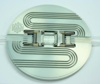
Click to EnlargeMay 24, 2011 — Sunrise Optical LLC debuted the Zebraoptical low coherence fiber optic interferometer with microscope attachment. The Zebraoptical Integrated Metrology Tool (ZIMT) provides metrology readings on micro electromechanical system (MEMS) wafers.

The tool’s standard Zebra wafer thickness and wafer topography metrology (ZebraOptical CT-IR) is paired with an optical microscope and VIS/NIR spectrometer. Users can measure substrate, membrane, and coating thicknesses and characterize coatings’ optical properties on the same tool platform.

A sample measurement service is available now. Learn more by contacting [email protected]. Lead time is currently 1 to 3 weeks ARO for the basic configuration.

Sunrise Optical LLC is an optical metrology company specializing in design and manufacturing of spectroscopic and imaging systems. www.zebraoptical.com.

Click to Enlarge
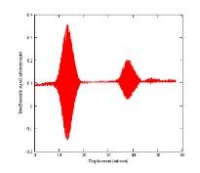
Zebraoptical Integrated Metrology Tool (ZIMT) interferometry measurement.

Follow Small Times on Twitter.com by clicking www.twitter.com/smalltimes. Or join our Facebook group

May 17, 2011 Wafer bonding is a complex process, used on 2" to 12" wafers for MEMS, CMOS image sensors, advanced packaging, LEDs, and other chips. Yole Développement published a technology study and market research report, "Permanent wafer bonding," to derive trends in the market and technology through 2016. The report aims at analyzing the market perspectives and technical trends for permanent bonding.

Yole Développement has estimated that the wafer bonding market will grow significantly for the next year. The growth will be driven small-size wafers for LEDs and 12" wafers for 3D die stacking and CIS.

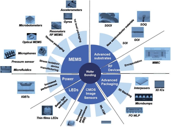
The wafer bonding market is a very complex one, crossing different wafer sizes (from 2" to 12"), different applications (MEMS, CMOS image sensors [CIS], LEDs, power devices, RF and advanced packaging), and different bonding technologies (adhesive, anodic, fusion, direct oxide, eutectic, glass frit, metal diffusion).

Click to Enlarge

Wafer bonding is usually defined as a process that temporarily or permanently joins two wafers or substrates using a suitable process. Historically developed for MEMS and then SOI wafers, wafer bonding technology has shifted to non-mainstream IC applications over the last years.

"MEMS has been the first application where wafer bonders have been massively used (the wafer bonding step is mostly used to protect the MEMS sensitive element), explained Dr Eric Mounier, project manager at Yole Développement. MEMS manufacturers are currently shifting from glass frit for eutectic/metal-based bonding, yielding smaller bond frames. Metal direct bonding also provides hermeticity and mechanical stability for many MEMS applications. For example, Nasiri uses eutectic bonding of the MEMS directly on the aluminum layer of the CMOS wafer. This leads to smaller package footprints & package heights. STMicroelectronics’ latest 3-axis accelerometer (LIS3DH) also shows a new sealing technique: gold eutectic sealing allows a dramatic die size reduction.

CMOS image sensors are also a strong wafer bonding application. Up to two different wafer bonding steps can be necessary for next-generation CMOS image sensor fab: one for back-side illumination, the second for wafer-level chipscale packaging (WLCSP). For CIS, the advent of backside illumination (BSI) technology has raised a competition between molecular bonding and adhesive bonding. Here, cost and final application will drive the final technology choice.

Besides MEMS and CIS manufacturing, wafer bonding also can be used for LED and power device fab. In a typical LED active region, spontaneous emission scatters photons in all directions. If the substrate material has a smaller band gap than the active region, approximately half of the light is absorbed in the substrate; significantly reducing device performance. So, one of the manufacturing solutions for photon loss involves bonding a wafer containing an array of devices to another wafer that provides both a reflective surface for maximum light extraction and a heatsink for thermal management.

Companies cited in the report:

Acreo, AML, APM/UMC, Avago, Ayumi, Bosch, Colibrys, Dalsa, Discera, EVGroup, FhG IMS, FLIR, IBM, Icemos, IMEC, IMT, Infineon, Infineon, Invensense, KTH, Leti, Lumileds, MEMStech, Micralyne, Mitsubishi Heavy Industries, Okmetic, Omron, Osram, Qualcomm, Raytheon, RPI, Sand9, Semefab, Sensonor, Silex, SOITEC, STM, SUSS MicroTEC, Tezzaron, TI, tMt, Tohoku University, TowerJazz, Tracit, Triquint, Tronic’s, TSMC, VTI, Xcom, Ziptronix

Over the 5 past years, much attention has been given to wafer bonding for 3D integration of memories, for example, and other die.

Although EV Group (EVG) is the market leader in permanent bonding, the growth of the bonding equipment market is attracting challengers.

Yole Développement’s report analyzes the technical & economical evolution of the permanent wafer bonding process. It gives 2010-2016 market forecasts for permanent bonding, equipment, an overview of the different bonding approaches and equipment players market shares and competitive information, This market & technology report also presents the trends for permanent bonding, wafer-to-wafer (W2W) vs. chip-to-wafer (C2W) analysis for 3D integration. It describes the applications for wafer bonding with main characteristics and challenges.
 
Report author:
Dr. Eric Mounier has a PhD in microelectronics from the INPG in Grenoble. Since 1998 he is a co-founder of Yole Développement, a market research company based in France. At Yole Développement, Dr. Eric Mounier is in charge of market analysis for MEMS, equipment & material. Yole Développement is a group of companies providing market research, technology analysis, strategy consulting, media in addition to finance services. Learn more at www.yole.fr

Subscribe to Solid State Technology/Advanced Packaging.

Follow Advanced Packaging on Twitter.com by clicking www.twitter.com/advpackaging. Or join our Facebook group

April 13, 2011 — Dolomite, microfluidic designer and manufacturer, launched a range of optical systems that capture high-quality still and moving images of microfluidic experiments.

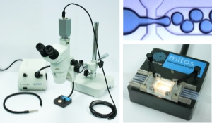
Click to EnlargeThe range of optical systems includes a high-speed camera and microscope system, providing a flexible solution for general microscopy including droplet generation and particle imaging. The system’s microscope offers zoom ratio of 7.5:1 and good working distance for a range of samples. The camera integrates with the microscope to capture images at over 1000 frames per second. The universal stand enables flexible microscope positioning.

The microscope stage is designed to accommodate all types of microfluidic chips and enables users to quickly locate and observe the area of interest. It can, for example, be used in conjunction with Dolomite’s Droplet Junction Chips for the improved visibility of droplet formation: droplet monodispersity, rate of production, and stability. The stage also features a 150W halogen cold light source with continuous dimming and no flicker effect at short exposure times.

Dolomite’s also offers a digital microscope that can be connected to a PC using a USB cable. The product is compact and low-cost for general microscopy, and Dolomite claims that it outweighs many of the USB microscopes currently available in image quality.

For further information on Dolomite’s range of Optical Systems as well as the complete portfolio of microfluidic products including chips, connectors/ interconnects, pumps, valves and custom devices, visit www.dolomitemicrofluidics.com.

Follow Small Times on Twitter.com by clicking www.twitter.com/smalltimes. Or join our Facebook group

April 7, 2011 — Agilent Technologies Inc. (NYSE: A) released Agilent NanoSuite 6.0, an enhanced-performance software package designed for use with Agilent Nano Indenter G200, G300 and T150 UTM systems. NanoSuite 6.0 promises speed, flexibility, ease of use and new application methods for nanomechanical properties measurements involving polymers, composites, thin film materials, MEMS, surface topology, stiffness mapping, and scratch testing.

NanoSuite 6.0 builds upon the intuitive interface, versatile imaging capabilities, survey scanning, and streamlined test-method development features introduced in the package’s previous iteration. The NanoSuite 6.0 software package offers several groundbreaking test methods, including an exclusive nanoindentation technique for substrate-independent measurements of thin film materials as well as test techniques for polymers.

To increase throughput and productivity, NanoSuite 6.0 facilitates the fast creation of new batches of tests for multiple samples. In addition to easily adding, editing, reviewing, or deleting samples, researchers can select a previously run batch of tests as a template for the current run. They can set up a standard batch of tests comprising 25 or more samples in five minutes or less.

NanoSuite 6.0 enables users to plot two-dimensional graphs, then export them directly to Microsoft Excel, with axis titles, scales, etc., exactly as they appeared on the monitor.

NanoSuite 6.0 also provides a new data structure that organizes sample files into projects and subprojects, Microsoft Windows 7 (32-bit) compliance for current systems, and a convenient PDF printer to replace hardware printers.

Agilent’s Nanoindentation instruments conform to the ISO 14577 standard. These state-of-the-art solutions ensure reliable, high-precision measurement of nanomechanical properties for research and industry. Agilent Technologies Inc. (NYSE: A) provides chemical analysis, life sciences, electronics and communications measurement products. Information about Agilent is available at www.agilent.com

Follow Small Times on Twitter.com by clicking www.twitter.com/smalltimes. Or join our Facebook group

March 8, 2011 – BUSINESS WIRE — IMT, wafer level packaging (WLP) company and MEMS foundry, introduced its hermetic gold-to-gold (Au-Au) thermo compression bonding. In development for nearly a year, this bond is being actively used in production, and it is said to be one of the lowest cost methods of achieving a hermetic wafer level package bond.

Low-temperate, low-cost wafer bonding could benefit MEMS packaging, as well as other applications.

In addition to the Au-Au thermo compression and the other bond technologies supported, IMT’s flagship remains its proprietary low-temperature hermetic eutectic bond. With sealing temperatures below 190°C and support for reflow temperatures of more than 500°C, this bond is ideal for temperature-sensitive sensors or electronics that require a hermetic package. The bond line width is controlled at less than 50µm.

"More than 80% of our total business makes use of wafer level packaging," said John Foster, IMT Chairman and CEO.

IMT produces and develops MEMS devices and is a pure-play MEMS foundry in the United States. IMT designs, manufactures, tests and supplies products to the RF, biotech, biomed, optical communications, infrared, navigation and general markets servicing Fortune 500 companies as well as startups. For more information, visit http://www.imtmems.com.

Subscribe to Solid State Technology/Advanced Packaging.

Follow Advanced Packaging on Twitter.com by clicking www.twitter.com/advpackaging. Or join our Facebook group

February 14, 2011 — Dolomite, microfluidic designer and manufacturer, expanded its range of temperature control systems with the Hotplate Adaptor – Chip Holder H, which allows control over internal temperatures of microfluidic chips without any disruptions to the fluid flow.

Click to Enlarge Click to Enlarge Click to Enlarge

The use of temperature control systems is vital for many applications including nanostructure generation, controlled microreactions, and droplet microfluidics where droplets can be kept at certain temperature to prevent a solidification reaction until the droplets have left the chip.

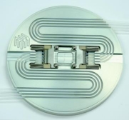
Holding a microfluidic chip securely in position, the Hotplate Adaptor enables users to pre-heat or post-heat fluids by using the integrated tube heater. Operating over a temperature range up to 100°C, the adaptor is supplied with a removable lid that can be closed to maintain the chip at constant temperatures, which is important for cell-based analytical studies to maintain cell viability. A glass viewing window (22mm in diameter) facilitates microscopic observations.

Quick and easy to use, the Hotplate Adaptor has been specifically developed for the Chip Interface H, and is compatible with Dolomite’s Linear Connector 4-way, 1.6mm tubing and microfluidic chips that have a footprint of 22.5 x 15mm.

Dolomite is pioneering the use of microfluidic devices for small-scale fluid control and analysis, enabling manufacturers to develop more compact, cost-effective and powerful instruments. By combining specialist glass, quartz and ceramic technologies with knowledge of high performance microfluidics, Dolomite is able to provide solutions for a broad range of application areas including environmental monitoring, clinical diagnostics, food and beverage, nuclear, agriculture, petrochemical, cosmetics, pharmaceuticals and chemicals. Dolomite’s in-house micro-fabrication facilities include clean rooms and precision glass processing facilities. For more information please visit www.dolomite-microfluidics.com

Follow Small Times on Twitter.com by clicking www.twitter.com/smalltimes. Or join our Facebook group

February 2, 2011 — Helios Crew Corporation (HCC) Taiwan released its LED product S35, a packaged component light-emitting diode (LED) that integrates MEMS with semiconductor processing to produce a unique silicon packaging technology.

Click to EnlargeIn conjunction with a high-brightness SemiLEDs chip, this compact size, silicon sub-mount technology delivers brightness and reliability. In addition, the S35 silicon has a thermal conductance more than 8 times higher than aluminum oxide ceramic packages, and at a considerably lower cost than aluminum nitride ceramic.

Helios Crew, Corporation is a subsidiary of SemiLEDs, Inc., a USA LED chip manufacturer traded on Nasdaq under the symbol LEDS. Learn more at www.helioscrew.com

Follow Small Times on Twitter.com by clicking www.twitter.com/smalltimes. Or join our Facebook group

January 24, 2011 — E M Optomechanical Inc. (EMOpto) developed a new low-cost version of its OPTOPro line of 3D MEMS Optical Profilers for use in testing and characterizing micro-electro-mechanical systems (MEMS) devices.

EMOpto introduced the latest in its line of dynamic 3D MEMS optical profilers, the OPTOPro Model 622-Xe, at less than $20K. It is based on exclusively licensed patented long-working distance interference microscopy technology.

"Feedback from potential customers indicates that tight budgets are preventing them from purchasing our higher priced models and that $20K would be a good price point for an entry level system," says Tom Swann, president of EMOpto. In addition to the Model 622-Xe, customers will have to provide a vibration isolation table, a structure to hold the profiler instrument and a means of holding and positioning the sample to be tested. "We have found that many prospective customers already have these capabilities available in-house," says Swann.

In addition to requiring the customer to furnish some of the system’s components, the low price was achieved by redesigning the mechanical portion of the profiler instrument and trimming the margin on software. "Even at its low price, the Model 622-Xe is a valuable and versatile research tool and it can accommodate a wide range of upgrades" says Swann.

EMOpto’s first generation line of products is intended primarily for use by micro-systems researchers for making real-time dynamic measurements of the micro- and nano-scale motions of MEMS devices and other micro-systems.

The technology behind EMOpto’s line of products was initially developed because there were no commercial optical profilers tailored specifically to the needs of micro-systems researchers. Its key feature is that it allows a long working distance without any sacrifice in measurement resolution. This allows capabilities not possible with other techniques such as allowing space for probes that are needed to attach to micro-system devices and viewing through portholes into vacuum chambers or through device cover glasses. Also read: Detecting failure modes in today’s MEMS

The profiler instrument is controlled by EMOpto’s MEMScript Software that also acquires and analyzes the data collected. This software has several unique features, such as the ability to control micro-system devices, which by nature have moving parts, and making real time measurements of performance. "MEMScriptTM" is a trademark of Sandia Corporation in the United States. Used with the permission of Sandia Corporation, and its licensee E M Optomechanical, Inc.

E M Optomechanical, Inc. was spun-off from Optomec, Inc. in 1998 to provide opto-mechanical engineering, design and fabrication services to the photonics industry. The Company has transitioned to a product oriented Company committed to commercialization of exclusively licensed patented long-working distance interference microscope technology for micro-systems research and development.

Follow Small Times on Twitter.com by clicking www.twitter.com/smalltimes. Or join our Facebook group

Executive Overview

Each year, several billion CMOS image sensors are manufactured to meet the growing demand for cameras in electronics products, notably camera phones, laptops (web cams) and now TVs. Fabricating device packages at the wafer-level provides economic advantage over discrete approaches since the materials and process costs are shared among the good die on the wafer, which can number many thousands for small die. Wafer-level packages also have the technical advantages of smaller dimensions, shorter interconnects and more consistent part-to-part performance. This article discusses the use of wafer-level packages, which satisfy the requirements.

Giles Humpston, Tessera Inc., San Jose, California, USA

Wafer-level packages for image sensors are unique on three counts. First is that the package must have an optically transparent window to permit light from the scene being imaged to reach the sensor. Second, the package has to provide environmental protection to the die in the form of stopping dust and dirt falling on the optically sensitive area. Third, image sensors can be made in two orientations, namely front-side illuminated and back-side illuminated, yet the same package is required to be compatible with both. Meeting these requirements has lead to the development of highly specialized, yet extraordinarily low cost, wafer-level packages for image sensors. It is predicted that by 2012 more than 70% of the image sensors produced annually will be housed in wafer-level packages.

Semiconductor device packaging

The traditional functions of a semiconductor device package are to protect the die from degradation by the atmosphere and fan-out the electrical interconnects to the next level. Because of the benign environment in which most modern semiconductors are used coupled with short expected life through product obsolescence, the need for the package to provide environmental protection has virtually disappeared. It is by no means uncommon to see essentially package-less chips attached to circuit boards, with just a polymer covering over the exposed bond pads. However, most semiconductor die are destined to interface to a printed circuit board (PCB) on which the pad size and pitch are fixed by standard, and hence, the package still has to provide the functions of redistribution and fan-out. For die larger than about 5mm on a side, it is also considered prudent for the package to incorporate a laterally compliant layer as part of the interconnect structure to act as a strain buffer. Because silicon has very low thermal expansivity, compared with common (PCB) materials, this layer works to confer acceptable fatigue life on the solder joints of the ball grid array that joins the package to the PCB.

Fabricating device packages at the wafer level provides economic advantage over discrete approaches since the materials and process costs are shared among the good die on the wafer. The benefit is most apparent when die are small and the wafers large so that many thousands or even tens of thousands can be processed simultaneously. Wafer-level packages also have the technical advantages of small footprint, the die and package having the same plan area; shorter interconnects, which permit faster operation/reduced power consumption; and more consistent part-to-part performance, reducing the need for test binning. Despite all of these benefits, development of wafer-level packages acceptable to industry has proved to be challenging and the majority of semiconductor devices are still housed in discrete packages.

Solid-state imagers

There are two principal types of solid-state image sensor, namely charge-coupled devices (CCD) and CMOS. CMOS imagers are able to function both optically and electronically, allowing for reduced size, lower power consumption and simplified assembly. Consequently, CMOS now dominates solid-state imager technology, except for niche applications where optical performance or imager resolution is paramount. Today, image sensor die are manufactured by many semiconductor companies. The smallest standardized area imager is the quarter common intermediate format (QCIF), with a resolution of 25,344 pixels, while the largest commercially available imager has 111 Mpixels.

Solid-state camera modules remained a relatively specialized product until 2001 when a common intermediate format (CIF) camera debuted on a mobile phone. Within eight years, the number of image sensors produced annually went from thousands to over 1 billion. It is estimated that in 2010, more than 80% of all mobile phones will have at least one camera, many having two. Other applications that use solid-state cameras include digital still cameras (DSC), camcorders, automotive driver aids, video security systems, web cams and increasingly, TVs. Together, these applications could consume an additional 1 billion camera modules per year by 2015.

The requirements of a package for a solid-state image sensor are not especially different from other semiconductor devices; the core needs remain a modicum of protection from the environment, redistribution and fan-out of the electrical interconnects, and absorption of thermal expansion mismatch. However, image sensors have one other requirement of the package, namely it must contain a transparent window to permit light to reach the optically active area of the die. The package must therefore contain a glass window − optically "transparent" polymers attenuate too much of the blue spectrum to be useful.

Early solid state imagers were housed in ceramic packages that were closed by a quartz cover slip. This solution, while perfectly functional, is wholly inadequate for high-volume manufacture and applications where the product cost and size are critical. Particular effort was therefore devoted to developing wafer-level packages for CMOS image sensors. This endeavor proved successful and it is predicted that by 2012, more than 70% of the image sensors produced annually will be housed in wafer-level packages.

Wafer-level image sensor package

A wafer-level package for an image sensor is relatively simple in concept (Fig. 1). A glass wafer is bonded to the front face of the die. Pathways are then formed to connect the die bond pads to a ball grid array interface on the underside of the package. Dicing frees individually packaged die. In reality, the structure and processes are considerably more complex.

Figure 1. Sequence of steps to manufacture a wafer level package for an image sensor. (Source: Tessera)

The first nuance is the glass wafer itself, which must be expansion-matched to silicon, extremely flat, thin, and free of even microscopic defects since it resides very close to the focal plane of the camera. It must also be available in conformance with SEMI standards. Few companies are able to make glass to the required specifications.

The second detail is that the glass wafer cannot be bonded to the surface of the silicon wafer. This is because the optically active area of the imager is covered with an array of microscopic lenses, one per pixel and typically 1-2µm high. These micro lenses are very fragile and cannot be cleaned. Any particle of dirt that lands on the micro lens array will stick, due to electrostatic attraction, blocking the incident light and causing a black spot in the image. The solution adopted is to form a picture frame around the micro lens array so that the glass wafer forms an optically transparent cover over the critical area. By attaching the glass wafer as the very first step in the packaging process, micro lenses are protected in their sealed cavity and any contamination that lands on the exterior surface of the glass can be easily removed.

While the glass cover provides protection to the micro lenses, it prohibits access to the die bond pads, which are rendered inaccessible beneath it. To contact the bond pads, some form of through-silicon via (TSV) must be employed. Despite being technically possible for over 30 years, TSVs have never been adopted in high-volume manufacturing. There are many contributory reasons for this, but they all adversely impact either cost, or reliability.

Figure 2. 300mm wafer and inset, single imager die housed in a wafer-scale package that uses a via-through-pad interconnect to join the die bond pads to the package lands and from there to the ball grid array interface. The interconnect is based on polymer technology with a single redistribution layer for the wiring trace. (Source: Tessera)

In contrast to most semiconductor die, image sensors have very low I/O counts for the die area. The die bond pads therefore tend to be large and widely spaced to aid process yield. By compromising on the complexity of the I/O redistribution carried by the package, it is possible to fabricate through-silicon vias based on polymer technology with a single metal layer for the wiring trace. This approach helps keep cost low and published reliability data show the package is suitable not just for portable electronics products, but able to surpass the far more exacting automotive reliability standard. A modern wafer-scale package for image sensors is shown in Fig. 2.

Sighting the TSVs over the bond pads means there are few restrictions on the bond pad size, pitch, or location. The dicing lanes can be as narrow as the silicon design rules allow, which helps to maximize the number of die per wafer and decrease unit cost. The total imager package imager thickness is approximately 500µm, making it imminently suitable for electronics products where the current fashion is for extreme thinness.

Back-illuminated image sensors

The vast majority of image sensors are front-side illuminated. That is, the light from the scene to be imaged falls on the processed face of the semiconductor, which is also the face on which the die bond pads are sited. Image sensors also come in another flavor, namely back-side illuminated, where the die is mounted inverted and the light falls on the unprocessed face of the semiconductor. This configuration yields superior performance in terms of quantum efficiency and reduced optical cross-talk, together with a reduction in the size of the corresponding camera module (Figs. 3a,b). The principal drawback of back-illuminated image sensors is higher manufacturing cost because additional and more complex processing is required. Hitherto, back-side illuminated image sensors tended to be reserved for scientific and aerospace applications.

Figure 3a. Schematic cross-section through a front-illuminated CMOS image sensor. For reasons based on physics the photo-detectors are buried 10-20µm deep in the silicon. The wiring trace that connects to each pixel is built on the surface of the wafer and is routed to minimize pixel obscuration. Nevertheless, the resulting aperture influences the maximum angle of captured incident light and also gives rise to a potential cross-talk mechanism. (Source: Tessera)

Recently, several companies have achieved breakthroughs in semiconductor processing that make back-illuminated image sensors possible for higher resolution imagers on mobile platforms where the attributes of high pixel count, good light sensitivity, and low camera module height are prized. However, the OEMs that integrate image sensors into their products do not want the problem and cost of a different style of package for each imager orientation. Back-illuminated imagers must therefore somehow be fit in wafer-level packages that have the same external structure as packages for front-illuminated imagers.

Figure 3b. Schematic cross-section through a back-illuminated CMOS image sensor. The die is fabricated in the conventional orientation, but the back silicon is then removed, exposing the photo detectors. Making the photo-detectors easily accessible to light trades manufacturing cost against performance and/or die size. (Source: Tessera)

Visible light is only able to penetrate a short distance into silicon. Therefore, in a back-illuminated imager, for photons to reach the photodiodes, the majority of the original wafer thickness must be removed. Clearly, there are basic handling and yield issues with 200mm or 300mm diameter silicon wafers that have been thinned to under 20µm. Mechanical support is provided by bonding a mechanical-grade silicon wafer to the original front face of the imager wafer. Back-illuminated imagers also use micro lens arrays, so a glass wafer, with closed cavities, is bonded to the light-sensitive side (the back side) of the device wafer. Thus, the bond pads are once again rendered inaccessible for wire bonding, being buried in the center of the glass-silicon-silicon sandwich.

The solution is to use TSV technology to access the bond pads. In this instance, the silicon through which the vias pass is the mechanical support wafer. Some subtle process changes are required to fabricate reliable interconnects to the bond pads on a back-illuminated die because of their inverted orientation. The net result is that the imager package can be made externally identical and the camera module manufacturer does not need to know whether it contains a front- or back-illuminated imager.

The better light sensitivity of back-illuminated image sensors can be put to a number of uses. One of these is to make the pixels, and thus the die smaller, since light-gathering ability is a function of the pixel area. Boosting the quantum efficiency from 25% to 70% permits the pixel size to be reduced from 2.6−1.5µm per side. For a VGA imager, this permits a wafer to accommodate around three times as many die−a reduction in unit cost that goes a long way toward offsetting the higher manufacturing and packaging cost of back-illuminated imagers.

Wafer-level package cost

Information on wafer-level package cost is difficult to obtain. However, one of the leading camera phone OEMs has published a target procurement cost for camera modules of $1 per megapixel. For a VGA camera, this means that only a few tens of cents are available to purchase a silicon die, two lenses, an infra-red filter, a light baffle and a housing for the optics, then assemble, test and ship the camera. The wafer-level package is also part of the bill of materials of the camera module, which implies that, to be in contention, the package cost per die must be extraordinarily low.

Biography

Giles Humpston received his PhD and BSc from Brunel U. (UK) and is Director, Applications (Europe) at Tessera, Inc., 3025 Orchard Parkway, San Jose, California, 95134, USA; ph.: 408-321-6000; email [email protected]

More Solid State Technology Current Issue Articles
More Solid State Technology Archives Issue Articles
(December 28, 2010) — The University of Michigan College of Engineering will present Packaging for MEMS March 31 to April 1, 2011, in Boston, MA. MEMS packaging is a significant part of product cost. This program highlights what to consider in developing application-specific packaging that will meet your goals for product performance, durability, and total cost.

Using the right MEMS packaging is critical for product sucess, point out the conference organizers. MEMS packaging is a significant part of product cost. This program highlights what to consider in developing application-specific packaging that will meet goals for product performance, durability, and total cost. Learn about extension of existing technology, exciting new technologies coming up, how to make MEMS packaging more specific to applications, and what’s going on in research. Examples of strengths and shortcomings of various packaging schemes are included.

The conference invites product design engineers and engineering managers of MEMS device manufacturers to attend, as well as engineers, managers, and system designers who use MEMS devices in their products.

This program is a joint presentation by U-M Electrical Engineering and Computer Science, The Center for Wireless Integrated MicroSystems (WIMS), and The Center for Professional Development.

Register online at www.InterPro.engin.umich.edu

The Center for Wireless Integrated Micro Systems (WIMS) is a world leader in developing packaging technology for a variety of MEMS systems. For more information about WIMS including education, research highlights, patents, and publications, see www.wimserc.org

Follow Small Times on Twitter.com by clicking www.twitter.com/smalltimes. Or join our Facebook group