Category Archives: Process Watch

DAVID W. PRICE, JAY RATHERT and DOUGLAS G. SUTHERLAND, KLA Corp., Milpitas, CA

The first three articles [1-3] in this series discussed methods that automotive semiconductor manufacturers can use to better meet the challenging quality requirements of their customers. The first paper addressed the impact of automotive IC reliability failures and the idea that combating them requires a “Zero Defect” mentality. The second paper discussed continuous improvement programs and strategies that automotive fabs implement to reduce the process defects that can become chip reliability problems. The third paper focused on the additional process control sensitivity requirements needed to capture potential latent (reliability) defects. This installment discusses excursion monitoring strategies across the entire automotive fab process so that non-conforming material can be quickly found and partitioned.

Semiconductor fabs that make automotive ICs typically offer automotive service packages (ASPs). These ASPs provide differentiated process flows – with elements such as more process control and process monitoring, or guaranteed use of golden process tools. The goal of ASPs is to help ensure that the chips produced meet the stringent reliability requirements of the automotive industry.

But even with the use of an automotive service package, excursions are inevitable, as they are with any controlled process. Recognizing this, automotive semiconductor fabs pay special attention to creating a comprehensive control plan for their critical process layers as part of their Process Failure Mode and Effects Analysis (PFMEA). The control plan details the process steps to be monitored and how they are monitored – specifying details such as the inspection sensitivity, sampling frequency and the exact process control systems to be used. A well-designed control plan will detect all excursions and keep “maverick” wafers from escaping the fab due to undersampling. Additionally, it will clearly indicate which wafers are affected by each excursion so that they can be quarantined and more fully dispositioned – thereby ensuring that non-conforming devices will not inadvertently ship.

To meet these objectives, the control plan of an automotive service package will invariably require much more extensive inspection and metrology coverage than the control plan for production of ICs for consumer products. An analysis of process control benchmarking data from fabs running both automotive and non-automotive products at the same design rule have shown that the fabs implement more defect inspection steps and more types of process control (inspection and metrology) for the automotive products. The data reveals that on average:

  • Automotive flows use approximately 1.5 to 2 times more defect inspection steps
  • Automotive flows employ more frequent sampling, both as a percentage of lots and number of wafers per lot
  • Automotive flows use additional sensitivity to capture the smaller defects that may affect reliability

The combined impact of these factors results in the typical automotive fab requiring 50% more process control capacity than their consumer product peers. A closer look reveals exactly how this capacity is deployed.

FIGURE 1 below shows an example of the number of lots between inspection points for both an automotive and a non-automotive process flow in the same fab. As a result of the increased number of inspection steps, if there is a defect excursion, it will be found much more quickly in the automotive flow. Finding the excursion sooner limits the lots at risk: a smaller and more clearly defined population of lots are exposed to the higher defect count, thereby helping serve the automotive traceability requirement. These excursion lots are then quarantined for high-sensitivity inspection of 100% of the wafers to disposition them for release, scrap, or when applicable, a downgrade to a non-automotive application.

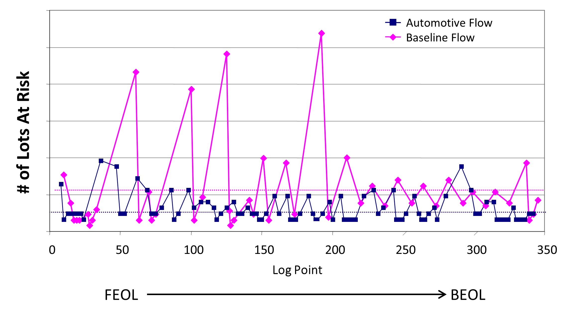
FIGURE 1. Example demonstrating the lots at risk between inspection points for an automotive process flow (blue) and a non-automotive (baseline) process blow (pink). The automotive process flow has many more inspection points in the FEOL and therefore fewer lots at risk when a defect excursion does occur.

The additional inspection points in the automotive service package have the added benefit of simplifying the search for the root cause of the excursion by reducing the range of potential sources. Fewer potential sources helps speed effective 8D investigations4 to find and fix the problem. Counterintuitively, the increased number of inspection points also tends to reduce production cycle time due to reduced variability in the line.5

While increasing inspection capacity helps monitor and contain process excursions, there remains risk to automotive IC quality. Because each wafer may take a unique path through the multitude of processing chambers available in the fab, the sum of minor variations and marginalities across hundreds of process steps can create “maverick” wafers. These wafers can easily slip through a control plan that relies heavily on sub-sampling, allowing at-risk die into the supply chain. To address this issue, many automotive fabs are adding high-speed macro defect inspection tools to their fleet to scan more wafers per lot. This significantly improves the probability of catching maverick wafers and preventing them from entering the automotive supply chain.

Newer generation macro defect inspection tools6 can combine the sensitivity and defect capture of many older generation brightfield and darkfield wafer defect inspection tools into a single platform that can operate at nearly 150 wafers per hour, keeping cost of ownership low. In larger design rule 200mm fabs, the additional capacity often reveals multiple low-level excursions that had previously gone undetected, as shown in FIGURE 2.

FIGURE 2. The legacy sample plan of 5 wafers per lot (yellow circles) would have allowed the single maverick wafer excursion (red square) to go undetected. High capacity macro defect inspection tools can stop escapes by reducing undersampling and the associated risks.

In advanced, smaller design rule fabs, macro defect inspection tools lack the needed sensitivity to replace the traditional line monitoring and patterned wafer excursion monitoring roles occupied by broadband plasma and laser scanning wafer defect inspection tools. However, their high capacity has found an important role in augmenting the existing sample plan to find wafer-level signatures that indicate a maverick wafer.

A recent development in automotive control strategies is the use of defect inspection for die-level screening. One such technique, known as Inline Defect Part Average Testing (I-PAT™), uses outlier detection techniques to further enhance the fab’s ability to recognize die that may pass electrical test but become reliability failures later due to latent defects. This method will be discussed in detail in the next installment of this series.

About the authors:

Dr. David W. Price and Jay Rathert are Senior Directors at KLA-Tencor Corp. Dr. Douglas Sutherland is a Principal Scientist at KLA-Tencor Corp.

References:

  1. Price, Sutherland and Rathert, “Process Watch: The (Automotive) Problem With Semiconductors,” Solid State Technology, January 2018.
  2. Price, Sutherland and Rathert, “Process Watch: Baseline Yield Predicts Baseline Reliability,” Solid State Technology, March 2018.
  3. Price, Sutherland, Rathert, McCormack and Saville, “Process Watch: Automotive Defect Sensitivity Requirements,” Solid State Technology, August 2018.
  4. 8D investigations involve a systematic approach to solving problems. https://en.wikipedia.org/wiki/Eight_disciplines_problem_solving
  5. Sutherland and Price, “Process Watch: Process Control and Production Cycle Time,” Solid State Technology, June 2016.
  6. For example, see: https://www.kla-tencor.com/products/chip-manufacturing/defect-inspection-review.html#product-8-series

A*STAR‘s Institute of Microelectronics (IME) and Lumerical Solutions, Inc. (Lumerical), a global provider of photonic design software, today announced they have co-developed a calibrated compact model library (CML) for IME’s silicon photonics platform and process design kit (PDK). The CML will help photonic integrated circuit (PIC) designers who use IME’s silicon photonics process to improve the accuracy and reliability of their designs.

IME’s 25G silicon photonics platform and PDK are built on validated processes and devices. They offer state-of-the-art performance and enable PIC designers to build reliable devices, system architectures and achieve prototyping and product manufacturing with ease.

PIC design is often manual and iterative, and is based on custom component libraries and workflows, which may lead to errors and multiple design revisions. Leveraging IME’s capabilities in silicon photonics process and device technology, and Lumerical’s expertise in integrated photonics device simulation and circuit design tools, the collaboration overcame these challenges by adding calibrated simulation models to IME’s silicon photonics PDK. The CML enables designers to accurately simulate and optimize the performance of complex PIC designs prior to fabrication.

The CML includes 15 active and passive elements, from waveguides to modulators and photo detectors, and forms part of IME’s silicon photonics PDK, along with process data, layer tables, cells for device layout and design rules.

“With silicon photonics emerging as a leading technology platform for high bandwidth optical communication, R&D is critical in addressing the industry’s needs for increasingly complex photonic-electronic circuits. I am confident that the combined strengths of IME’s capabilities in silicon photonics technologies for integration and manufacturing, and Lumerical’s experience in innovating design tools will enable designers to produce quality photonic integrated circuits, and accelerate the production of next generation devices”, said Prof. Dim-Lee Kwong, Executive Director, IME.

“The addition of calibrated models to IME’s photonic PDK is a compelling step forward in establishing the design and fabrication ecosystem necessary for photonic circuit designers to realise the commercial potential of integrated photonic technologies,” stated Todd Kleckner, co-founder and Chief Operating Officer, Lumerical. “We are excited to work with a renowned and innovative research institute like IME and support joint users of IME’s MPW services and our design tools to confidently scale design complexity and deliver on their next ambitious design challenge.”


When a 300mm wafer is vacuum mounted onto the chuck of a scanner, it needs to be flat to within about 16nm over a typical exposure field, for wafers intended for 28nm node devices.1 A particle as small as three microns in diameter, attached to the back side of the wafer—the dark side, if you will—can cause yield-limiting defects on the front side of the wafer during patterning of a critical layer. The impact of back side particles on front side defectivity becomes even more challenging as design rules decrease.

Studies have shown that a relatively incompressible particle three microns in diameter or an equivalent cluster of smaller particles, trapped between the chuck and the back surface of the wafer, can transmit a localized height change on the order of 50nm to the front side of the wafer.2 With the scanner’s depth-of-focus reduced to 50nm for the 28nm node, the same back side particle or cluster can move the top wafer surface outside the sweet spot for patterning. The CD of the features may broaden locally; the features may be misshapen. The result is often called a defocus defect or a hotspot (Figure 1). These defects are frequently yield-limiting because they will result in electrical shorts or opens from the defective feature to its neighbors.

A particle on the back side of the wafer may remain attached to the wafer, affecting the yield of only that wafer, or it may be transferred to the scanner chuck, where it will create similar defects on the next wafer or wafers that pass through the scanner.

At larger design nodes, back side defects were not much of an issue. The scanner’s depth of focus was sufficient to accommodate a few microns of localized change in the height of the top surface of the wafer. At larger design nodes, then, inspection of the back side of the wafer was performed only after the lithography track and only if defects were found on successive wafers, indicating that the offending particle remained on the scanner chuck, poised to continue to create yield issues for future wafers. In this case corrective measures were undertaken on the track to remove any suspected contamination. The track was re-qualified by sending another set of wafers through it and looking for defectivity at the front side locus of the suspected back side particle. This reactive approach was economically feasible for most devices throughout volume production of 32nm devices.

At the 28nm node, however, lithography process window requirements are such that controlling back side particles requires a more proactive approach. Advanced fabs now tend to inspect the wafer back side before the wafer enters the scanner, heading off any potential yield loss. Scanner manufacturers are also encouraging extensive inspection of the back side of wafers before they enter the track. As we see what lithography techniques unfold for the 16nm, 10nm nodes and beyond, it’s entirely possible that 100% wafer sampling will become the best-known method.

As with inspection of the front side of the wafer, sensitivity to defects of interest (DOI) and the ability to discriminate between DOI and nuisance events are important. Even though particles need to be two to three microns in diameter before they have an impact on front side defectivity, the inspection system ought to be able to detect sub-micron defects, since small defects can agglomerate to form clusters of critical size. Sub-micron sensitivity is beneficial for identifying process tool issues based on the spatial signature of the defects—while high-resolution back side review enables imaging of localized defects, so that appropriate corrective actions can be taken to protect yield. Sub-micron sensitivity also serves to extend the tool’s applicability for nodes beyond 28nm.

For further information on back side inspection equipment or methodologies, please consult the second author.

Rebecca Howland, Ph.D., is a senior director in the corporate group, and Marc Filzen is a product marketing manager in the SWIFT division at KLA-Tencor.

Check out other Process Watch articles: “The Dangerous Disappearing Defect,” “Skewing the Defect Pareto,” “Bigger and Better Wafers,” “Taming the Overlay Beast,” “A Clean, Well-Lighted Reticle,” “Breaking Parametric Correlation,” “Cycle Time’s Paradoxical Relationship to Yield,” and “The Gleam of Well-Polished Sapphire.”

Notes:

1.       Assuming 193nm exposure wavelength, NA = 1.35 and K2 = 0.5, then depth of field = 50nm. Normally 30% of the DOF is budgeted for wafer flatness.

2.       Internal studies at KLA-Tencor.

By Rebecca Howland, Ph.D., and Tom Pierson, KLA-Tencor.

Is it time for high-brightness LED manufacturing to get serious about process control?  If so, what lessons can be learned from traditional, silicon-based integrated circuit manufacturing?

The answer to the first question can be approached in a straight-forward manner: by weighing the benefits of process control against the costs of the necessary equipment and labor.  Contributing to the benefits of process control would be better yield and reliability, shorter manufacturing cycle time, and faster time to market for new products. If together these translate into better profitability once the costs of process control are taken into account, then increased focus on process control makes sense.

Let’s consider defectivity in the LED substrate and epi layer as a starting point for discussion. Most advanced LED devices are built on sapphire (Al2O3) substrates. Onto the polished upper surface of the sapphire substrate an epitaxial (“epi”) layer of gallium nitride (GaN) is grown using metal-organic chemical vapor deposition (MOCVD).

Epitaxy is a technique that involves growing a thin crystalline film of one material on top of another crystalline material, such that the crystal lattices match—at least approximately. If the epitaxial film has a different lattice constant from that of the underlying material, the mismatch will result in stress in the thin film. GaN and sapphire have a huge lattice mismatch (13.8%), and as a result, the GaN “epi layer” is a highly stressed film. Epitaxial film stress can increase electron/hole mobility, which can lead to higher performance in the device. On the other hand, a film under stress tends to have a large number of defects.

Common defects found after deposition of the epi layer include micro-pits, micro-cracks, hexagonal bumps, crescents, circles, showerhead droplets and localized surface roughness. Pits often appear during the MOCVD process, correlated with the temperature gradients that result as the wafer bows from center to edge. Large pits can short the p-n junction, causing device failure. Submicron pits are even more insidious, allowing the device to pass electrical test initially but resulting in a reliability issue after device burn-in. Reliability issues, which tend to show up in the field, are more costly than yield issues, which are typically captured during in-house testing. Micro-cracks from film stress represent another type of defect that can lead to a costly field failure.

Typically, high-end LED manufacturers inspect the substrates post-epi, taking note of any defects greater than about 0.5mm in size. A virtual die grid is superimposed onto the wafer, and any virtual die containing significant defects will be blocked out. These die are not expected to yield if they contain pits, and are at high risk for reliability issues if they contain cracks. In many cases nearly all edge die are scrapped. Especially with high-end LEDs intended for automotive or solid-state lighting applications, defects cannot be tolerated: reliability for these devices must be very high.

Not all defects found at the post-epi inspection originate in the MOCVD process, however. Sometimes the fault lies with the sapphire substrate. If an LED manufacturer wants to improve yield or reliability, it’s important to know the source of the problem.

The sapphire substrate itself may contain a host of defect types, including crystalline pits that originate in the sapphire boule and are exposed during slicing and polishing; scratches created during the surface polish; residues from polishing slurries or cleaning processes; and particles, which may or may not be removable by cleaning. When these defects are present on the substrate, they may be decorated or augmented during GaN epitaxy, resulting in defects in the epi layer that ultimately affect device yield or reliability (see figure).

Patterned Sapphire Substrates (PSS), specialized substrates designed to increase light extraction and efficiency in high-brightness LED devices, feature a periodic array of bumps, patterned before epi using standard lithography and etch processes. While the PSS approach may reduce dislocation defects, missing bumps or bridges between bumps can translate into hexes and crescent defects after the GaN layer is deposited. These defects generally are yield-killers.

In order to increase yield and reliability, LED manufacturers need to carefully specify the maximum defectivity of the substrate by type and size—assuming the substrates can be manufactured to those specifications without making their selling price so high that it negates the benefit of increased yield. LED manufacturers may also benefit from routine incoming quality control (IQC) defect measurements to ensure substrates meet the specifications—by defect type and size.

Substrate defectivity should be particularly thoroughly scrutinized during substrate size transitions, such as the current transition from four-inch to six-inch LED substrates. Historically, even in the silicon world, larger substrates are plagued initially by increased crystalline defects, as substrate manufacturers work out the mechanical, thermal and other process challenges associated with the larger, heavier boule.

A further consideration for effective defect control during LED substrate and epi-layer manufacturing is defect classification. Merely knowing the number of defects is not as helpful for fixing the issue as knowing whether the defect is a pit or particle. (Scratches, cracks and residues are more easily identified by their spatial signature on the substrate.) Leading-edge defect inspection systems such as KLA-Tencor’s Candela products are designed to include multiple angles of incidence (normal, oblique) and multiple detection channels (specular, “topography,” phase) to help automatically bin the defects into types. For further information on the inspection systems themselves, please consult the second author.

Rebecca Howland, Ph.D., is a senior director in the corporate group, and Tom Pierson is a senior product marketing manager in the Candela division at KLA-Tencor.

Check out other Process Watch articles: “The Dangerous Disappearing Defect,” “Skewing the Defect Pareto,” “Bigger and Better Wafers,” “Taming the Overlay Beast,” “A Clean, Well-Lighted Reticle,” “Breaking Parametric Correlation,” “Cycle Time’s Paradoxical Relationship to Yield,” and “The Gleam of Well-Polished Sapphire.”

In an IC fab, cycle time is the time interval between when a lot is started and when it is completed. The benefits of shorter cycle time during volume production are well known: reduced capital costs associated with having less work in progress (WIP); reduced number of finished goods required as safety stock; reduced number of wafers affected by engineering change notices (ECNs); reduced inventory costs in case of a drop in demand; more flexibility to accept orders, including short turnaround orders; and shorter response time to customer demands. Additionally, during development and ramp, shorter cycle times accelerate end-of-line learning and can result in faster time to market for the first lots out the door.

Given all the benefits of reducing cycle time, it’s useful to consider how wafer defect inspection contributes to the situation. To begin with, the majority of lots do not accrue any cycle time associated with the inspection, since usually less than 25 percent of lots go through any given inspection point. For those that are inspected, cycle time is accrued by sending a lot over to the inspection tool, waiting until it’s available, inspecting the lot and then dispositioning the wafers. On the other hand, defect inspection can decrease variability in the lot arrival rate—thereby reducing cycle time.

Three of the most important factors used in calculating fab cycle time are variability, availability, and utilization. Of these, variability is by far the most important. If lots arrive at process tools at a constant rate, exactly equal to the processing time, then no lot will ever have to wait and the queue time will be identically zero. Other sources of variability affect cycle time, such as maintenance schedules and variability in processing time, but variability in the lot arrival rate tends to have the biggest impact on cycle time.

In the real world lots don’t arrive at a constant rate and one of the biggest sources of variability in the lot arrival rate is the dreaded WIP bubble—a huge bulge in inventory that moves slowly through the line like an over-fed snake. In the middle of a WIP bubble every lot just sits there, accruing cycle time, waiting for the next process tool to become available. Then it moves to the next process step where the same thing happens again until eventually the bubble dissipates. Sometimes WIP bubbles are a result of the natural ebb and flow of material as it moves through the line, but often they are the result of a temporary restriction in capacity at a particular process step (e.g., a long “tool down”).

When a defect excursion is discovered at a given inspection step, a fab may put down every process tool that the offending lot encountered, from the last inspection point where the defect count was known to be in control, to the current inspection step.  Each down process tool is then re-qualified until, through a process of elimination, the offending process tool is identified.

If the inspection points are close together, then there will be relatively few process tools put down and the WIP bubble will be small.  However, if the inspection points are far apart, not only will more tools be down, but each tool will be down for a longer period of time because it will take longer to find the problem.  The resulting WIP bubble can persist for weeks, as it often acts like a wave that reverberates back and forth through the line creating abnormally high cycle times for an extended period of time. 

Consider the two situations depicted in Figure 1 (below). The chart on the top represents a fab where the cycle time is relatively constant. In this case, increasing the number of wafer inspection steps in the process flow probably won’t help.  However, in the second situation (bottom), the cycle time is highly variable. Often this type of pattern is indicative of WIP bubbles.  Having more wafer inspection steps in the process flow both reduces the number of lots at risk, and may also help reduce the cycle time by smoothing out the lot arrival rate.


Because of its rich benefits, reducing cycle time is nearly always a value-added activity. However, reducing cycle time by eliminating inspection steps may be a short-sighted approach for three important reasons. First, only a small percentage of lots actually go through inspection points, so the cycle time improvement may be minimal. Second, the potential yield loss that results from having fewer inspection points typically has a much greater financial impact than that realized by shorter cycle time. Third, reducing the number of inspection points often increases the number and size of WIP bubbles. 

For further discussions on this topic, please explore the references listed at the end of the article, or contact the first author.

Doug Sutherland, Ph.D., is a principal scientist and Rebecca Howland, Ph.D., is a senior director in the corporate group at KLA-Tencor.

Check out other Process Watch articles: “The Dangerous Disappearing Defect,” “Skewing the Defect Pareto,” “Bigger and Better Wafers,” “Taming the Overlay Beast,” “A Clean, Well-Lighted Reticle,” “Breaking Parametric Correlation,” “Cycle Time’s Paradoxical Relationship to Yield,” and “The Gleam of Well-Polished Sapphire.”

References

1.       David W. Price and Doug Sutherland, “The Impact of Wafer Inspection on Fab Cycle Time,” Future Technology and Challenges Forum, SEMICON West, 2007.

2.       Peter Gaboury, “Equipment Process Time Variability: Cycle Time Impacts,” Future Fab International. Volume 11 (6/29/2001).  

3.       Fab-Time, Inc.  “Cycle Time Management for Wafer Fabs:  Technical Library and Tutorial.”

4.       W.J. Hopp and M.L. Spearman, “Factory Physics,” McGraw-Hill, 2001, p 325.

When you’re designing a geometrically complex structure like a high-k metal gate, FinFET, or vertical DRAM, you will probably use SEM/TEM cross-sectional imaging to work out the bugs. Maybe even a touch of AFM. However, in production, optical scatterometry-based technology is used, chosen for its speed, non-destructive nature and ability to monitor the 3D shape of a feature. This group of metrology techniques is commonly called OCD (Optical Critical Dimension) or SCD (Scatterometry Critical Dimension).

SCD tools commonly employ either reflectometry, ellipsometry, or a combination of the two methods.  In both approaches, the tool focuses a beam of light onto the structure and collects the light that bounces back. By varying the wavelength, a spectrum is constructed that can be sensitive to the shape of the structure, to the optical properties of the materials that comprise the structure, and to previous-layer features buried within materials transparent at the measurement wavelength.

For a given structure and SCD measurement setup, a set of modeled spectra are generated (either on the fly, or offline and stored as a library of curves) that characterize how the spectrum would change if a parameter of interest were varied—for example, the depth of a trench in a vertical DRAM. The measured spectrum is then compared to the modeled spectra to determine which of the models fits best. The result should correspond to a precise, repeatable value for the parameter of interest.

Of course, seldom is anything that simple in real life. Sometimes more than one parametric change (e.g. trench depth and top CD) results in about the same change in the spectrum. The SCD community calls this phenomenon “parametric correlation.”

Let’s say SCD is being used to monitor the shape of a high-k metal gate structure in production

(Figure 1). Suppose the metal undercut, metal and silicon layer bottom CDs and the silicon sidewall angle are the parameters of interest; various failure analysis techniques have shown that small variations in these parameters can correspond to significant degradation in device performance or yield. Let’s also say that small variations in the undercut length are evident in the SCD spectrum—but in a way that’s indistinguishable from what happens when the metal bottom CD changes. A similar issue was reported by GLOBALFOUNDRIES and IBM, in a paper published in a recent SPIE Proceedings on Advanced Lithography.1 


How can you unravel which structural or material variation is causing the change in the spectrum in the presence of parametric correlation? It’s easy if you are certain that one of the two correlated parameters is well controlled—and therefore you can assume that the other parameter is changing. Unfortunately, this is not always the case.

A related way to reduce the variables in the problem is by carrying data forward from previous layers.  If the results for a given layer on a given wafer have already been determined, that information can be used to “fix” the values of some parameters in new layers.  This capability is available today if the wafer has been consistently measured on the same SCD tool. In the future it will be possible to extend this capability to wafers measured on different SCD tools within a fab—as long as those tools are well matched.

When it’s not possible to remove variables by fixing their values, parametric correlation can often be broken by changing the type of SCD measurement: using a different wavelength range; sending the light in at a different azimuth or altitude angle; changing the polarization; or using ellipsometry instead of reflectometry or vice versa. If you have enough different technologies to throw at the problem, you may find one setup that allows the SCD tool to respond sensitively to one of the correlated parameters and not the other.  Sometimes it’s necessary to combine spectra from multiple technologies (angles, polarizations, etc.) or from measuring multiple structures (vertical and horizontal lines, or isolated and dense lines) to come up with a unique solution.

In the example cited earlier, GLOBALFOUNDRIES and IBM found that the use of multiple azimuth angles (parallel and perpendicular to the direction of the dominant lines and spaces) allowed SCD to monitor variations in the metal undercut with high precision and repeatability—and low parametric correlation.

Rebecca Howland, Ph.D., is a senior director in the corporate group and Lanny Mihardja is a product marketing manager in the Films and Scattering Technology (FaST) Division at KLA-Tencor.

Check out other Process Watch articles: “The Dangerous Disappearing Defect,” “Skewing the Defect Pareto,” “Bigger and Better Wafers,” “Taming the Overlay Beast,” “A Clean, Well-Lighted Reticle,” “Breaking Parametric Correlation,” “Cycle Time’s Paradoxical Relationship to Yield,” and “The Gleam of Well-Polished Sapphire.”

References

1.       Matthew Sendelbach, Alok Vaid, Pedro Herrera, Ted Dziura, Michelle Zhang and Arun Srivatsa, “Use of multiple azimuthal angles to enable advanced scatterometry applications,“ Metrology, Inspection, and Process Control for Microlithography XXIV, ed. Christopher J. Raymond, Proc. of SPIE Vol. 7638, 76381G, 2010.

When something happens to a reticle, the consequences can be dire. Contamination in the wrong place on a reticle can result in a defect in every die of every wafer. Fabs have to keep their reticles clean.

On the other hand, if the reticle is cleaned too many times, the pattern can start to erode. Reticle pattern degradation eventually causes critical dimension uniformity (CDU) changes on the wafer, which can translate into issues of device performance or yield. Plus, while the reticle is going through the cleaning process, it’s not available to do its work in the scanner.  Unless reticle cleaning is carefully planned, production of that particular product may screech to a halt. Fabs need to check their reticles for contamination and pattern degradation—at a frequency that balances the cost of taking the reticle offline to inspect it and the cost of the inspection itself against the risk of printing reticle defects or CDU errors on the wafer.

Some fabs have moved their reticle cleaning facilities on site, greatly accelerating the turnaround time to get the reticle cleaned, re-inspected, and back online. New cleaning technologies have also come into favor, including wet processes like UV-ozonated water with hydrogen peroxide, and dry processes including plasma and laser shot cleaning. In general the new processes have resulted in reduced overall defectivity post-clean; however, the problem of pattern erosion remains, and the remaining defects can be more difficult to detect.

Recent studies1 have shown that contamination is more likely to occur at the edges of mask pattern features than in open areas between features. That’s bad news for the wafers, because a variation on the edge of the mask pattern will immediately affect the carefully engineered wavefronts of the light that transfers the mask pattern to the photoresist on the wafer. It’s also bad news for the reticle defect inspectors, because it’s much more difficult to detect a defect in an area of dense pattern than a defect the same size, sitting in the middle of an unused space. Also, the mask error enhancement factor (MEEF) of a defect within dense pattern is higher than that of a defect in open space—which means that the defect within the pattern is more likely to print on the wafer and more likely to affect die yield. It may be difficult to find defects on the edge of pattern, but these defects have the potential to be the most damaging. They must be found.

In the mask shop, reticle inspection is accomplished by comparing the pattern on the mask to the design information—a “die-to-database” inspection. In the IC fab, the mask database is often not available. For that reason, KLA-Tencor invented a database-free method for detecting contamination on a mask, a method called STARlightTM, named for its use of Simultaneous Transmitted And Reflected light. First introduced in 1995, the STARlight methodology2 compares the transmitted-light and reflected-light images of a reticle to determine whether or not a defect is present. Since then, STARlight has undergone many improvements, and today’s fifth-generation STARlight is optimized for detecting defects on edges of pattern features.

1. STARlight operated on the simultaneous transmitted (left) and reflected (middle) image to identify the defect (right).

STARlight addresses the issue of finding localized contaminants, even on pattern edges. It works for single-die, multi-die or shuttle masks (multi-die masks comprised of different die), inspecting any kind of random or repeating pattern—including the scribe line. Once these defects are found, the reticle can be cleaned and re-used.  But what happens when the cleaning process is modifying or removing pattern—material that’s supposed to be there—instead of contaminants?  Or what if the problem is not localized contamination, but a contaminating film that affects the reticle’s transmissivity? These issues may not create defects on the wafer, but they may affect the wafer’s CDU.

Some inspection systems now offer a mode that maps the reflectivity or transmissivity across the entire reticle. In some cases, these data are collected simultaneously with localized defect data. The reticle maps can then be processed and calibrated against a reference to extract CDU information.

2. Examples of intensity-based CDU maps from the reticle inspection system.

3. Degradation of a sub-resolution assist feature (SRAF), imaged by the reticle inspection system.

With the introduction of new cleaning processes and smaller pattern features, reticle management in the IC fab has extended beyond detection of localized defects to include detection of contaminating films and CDU changes. With thoughtful sampling strategies, regularly inspected reticles can live long, productive lives.

Rebecca Howland, Ph.D., is a senior director in the corporate group and Mark Wylie is a product marketing manager in the Reticle Products Division at KLA-Tencor.

Check out other Process Watch articles: “The Dangerous Disappearing Defect,” “Skewing the Defect Pareto,” “Bigger and Better Wafers,” “Taming the Overlay Beast,” “A Clean, Well-Lighted Reticle,” “Breaking Parametric Correlation,” “Cycle Time’s Paradoxical Relationship to Yield,” and “The Gleam of Well-Polished Sapphire.”

References

1. E. Foca, A. Tchikoulaeva, B. Sass, C. West, P. Nesladek, R. Horn, “New type of haze formation on masks fabricated with Mo-Si blanks,” Photomask Japan 2010.

2. F. Kalk, D. Mentzer, A. Vacca, “Photomask production integration of KLA STARlight 300 system,” Proc. SPIE 2621, 15th Annual BACUS Symposium on Photomask Technology and Management 112 (1995).


Overlay error is the offset in alignment between pattern at one step of a semiconductor process and pattern at the next step. Traditionally overlay error has referred to successive device layers, but in the case of double-patterning lithography, overlay error may stem from interwoven patterns at the same layer. Regardless, controlling overlay error is one of the most difficult issues that lithography engineers face in this era of shrinking design rules and complex, advanced lithography techniques. Because overlay error can affect yield, device performance and reliability, it must be measured precisely, and all sources of systematic overlay error must be discovered and addressed. These may include mask pattern placement error, deviations from wafer planarity, scanner nonlinearities and process variation.

In most cases, overlay error is measured optically by capturing an image of a specially designed alignment mark called an overlay target. Half of the overlay target is printed during the first process step, and the other half of it is printed during the second process step.


A standard overlay target is printed in two steps,  indicated in red and blue, and structured to measure the errors in x and y.

An overlay metrology tool captures the image and quantifies the alignment between the first and second parts of the target. The result is reported as a vector quantity, having a magnitude and direction corresponding to the x and y offsets. The procedure is repeated for each of the overlay targets on the wafer. Overlay error maps are comprised of a circular field of tiny vectors, representing the overlay error across the wafer. These maps are used to adjust the scanner or to uncover issues with the mask pattern, the wafer shape or the process. Overlay error maps are also used to disposition wafers.

Flexible, robust multi-layer target allows simultaneous measurement of overlay error within the same layer and between layers.

A recent development in the area of overlay measurement is extension of measurement capability to new layers and new materials (see above). When overlay error between layers is measured, the optical properties of the top layer are critical to the quality of the data. The metrology tool needs to be able to send photons through the top layer to detect the pattern underneath, and the quality of the image of the buried pattern is critical to the quality of the overall measurement. Because semiconductor processes use a variety of materials, and the optical absorption of a given material generally varies with wavelength, the well-equipped metrology system can select from a variety of wavelengths to achieve sufficient image quality for the buried pattern to enable an accurate, repeatable measurement. The alternative—introducing an extra process step to etch a “window” in the top layer before patterning it—adds significant cycle time and may degrade the underlying pattern. Cycle time pressures are ever-present and well known. Furthermore, when the entire overlay error budget is limited to a small number of nanometers, lithographers cannot afford to allot a large portion of the budget to uncertainty in the output of the overlay metrology tool.

Examples of particularly challenging classes of materials are those used to build 3D transistors, and hard mask materials used during litho-etch-litho-etch lithography. Hard mask materials are opaque to visible light, and their optical properties may fluctuate with composition and even with annealing temperature.  The latest overlay metrology systems can provide an appropriate wavelength that penetrates the top layer, making overlay metrology feasible without additional process steps.

Another new development in the field of overlay metrology is the use of multi-layer overlay targets. New target designs now allow a lithography engineer to measure within-layer overlay and between-layer overlay using one target. These innovative targets are small enough to be inserted into the die without consuming an unfeasible amount of valuable real estate. Their designs are flexible and robust, allowing adjustments for specific process and layer requirements. They are compatible with various pitch-splitting and double-patterning schemes. Most importantly, the new multi-layer targets allow lithographers to measure within- and between-layer overlay error with one image and, at the same time, reduce systematic errors that could degrade the measurement if separate targets had been used.

Overlay metrology remains one of the most challenging issues that lithographers currently face. Innovations in overlay metrology tool and target design must continue, to enable our industry to make smaller, faster, lower power, more affordable chips.

Rebecca Howland, Ph.D., is a senior director in the corporate group and Amir Widmann is a senior director in the Optical Metrology division at KLA-Tencor.

Check out other Process Watch articles: “The Dangerous Disappearing Defect,” “Skewing the Defect Pareto,” “Bigger and Better Wafers,” “Taming the Overlay Beast,” “A Clean, Well-Lighted Reticle,” “Breaking Parametric Correlation,” “Cycle Time’s Paradoxical Relationship to Yield,” and “The Gleam of Well-Polished Sapphire.”

In the third installment in a series called Process Watch, the authors discuss some of the challenges of 450mm wafers. Authored by experts at KLA-Tencor, Process Watch articles focus on novel process control solutions.

August 2, 2012 — Chip manufacturers need wafers that are both bigger and better: bigger to help achieve cost targets through gains in manufacturing efficiency, and better to help reach device performance targets through the time-honored path of the pattern shrink. Our industry leaders have announced plans for pilot lines producing devices with sub-20nm linewidths on 450mm wafers, beginning in 2014 or 2015.

In the meantime, wafer manufacturers need to figure out how to make these giant wafers. The increased time required to grow the huge silicon ingot and then to cool it down under conditions optimized for crystal quality raises the risk of defects in the silicon crystal significantly.1 Polishing the surface uniformly and without microscratches requires new equipment and consumables. New cleaning equipment and processes must be developed. Also, 450mm wafers are proportionally thinner than 300mm wafers — which means they are more likely to deform during processing or handling. Such deformation can induce slip lines — crystal lattice defects similar to geological slip lines after an earthquake — around the edge of the large wafer. Crystal-originated pits (COPs), particles, slip lines, microscratches and cleaning residues all can interfere with one or more of the tightly-controlled processes that comprise the early steps of building a semiconductor device.

Printing smaller patterns necessitates tighter specs on many aspects of the wafer — regardless of wafer size. Because 450mm wafers will be used for sub-20nm lithography, their flatness and surface roughness must be very well controlled. Gradual changes in the shape of the wafer surface can be corrected by the scanner during patterning, but the wafer must be reasonably planar across the reticle field. More abrupt changes in the shape of the wafer surface may not be correctable; this is termed higher-order shape. Uncorrectable higher-order shape can displace the pattern, resulting in misalignment (overlay error) between layers — or it can cause defocus errors that affect the critical dimension (CD) of the printed structures. Higher-order shape can also interfere with film uniformity during chemical-mechanical polish (CMP) processes. Any of these errors can result in electrical problems affecting the device’s reliability, performance or yield.

450mm wafers have a higher number of edge die — notoriously the lowest yielding die on the wafer. The shape of the edge (“Edge Roll-Off” or ERO) can affect CD during patterning of edge die. Defectivity at and near the edge of 450mm wafers is typically higher, and will need to be very carefully monitored.

In essence, substrate manufacturers need to make much larger wafers with surfaces even more perfect than they are now: truly bigger and better wafers.  The impact of the surface quality, defectivity, flatness and ERO of 450mm wafers is considerable: With more than twice the number of die as a 300mm wafer, every 450mm wafer is extremely valuable. And just to add an extra challenge, some industry pioneers have announced that they will manufacture devices on 450mm epi wafers — adding the complexity of an epitaxial silicon layer, with its slightly increased surface roughness, stress-induced warp and unique epi defects. There is also interest in validation of 450mm silicon-on-insulator (SOI) technology.

Bare-wafer metrology and defect inspection play key and early parts in enabling wafer, equipment and chip manufacturers to develop and control their sub-20nm processes on 450mm wafers. These tools need the sensitivity to meet sub-20nm node requirements, and the ability to handle 450mm wafers with reliability and speed. Sub-20nm inspection sensitivity is enabled by deep-ultraviolet (DUV) technology and high-resolution haze mapping, technology that was pioneered recently on 300mm wafers by the latest-generation surface inspection systems. The images below show examples of surface defects, polishing marks and cleaning residues revealed on 450mm wafers by the latest inspection technology. These images are visually interesting, but indicative of the early stages of the manufacturing process; images of wafers meeting chip manufacturing specs would look nearly uniform. High resolution surfaces images such as these are a quick and intuitive tool for identifying the source of the defect, so that the issue can be remedied immediately, before additional time and materials are consumed.


Rebecca Howland, Ph.D., is a senior director in the corporate group and Amir Azordegan, Ph.D., is a senior director in the Surfscan/ADE division at KLA-Tencor.

1. See for example, “Technical challenges in the development of next generation wafers.”.

Check out other Process Watch articles: “The Dangerous Disappearing Defect,” “Skewing the Defect Pareto,” “Bigger and Better Wafers,” “Taming the Overlay Beast,” “A Clean, Well-Lighted Reticle,” “Breaking Parametric Correlation,” “Cycle Time’s Paradoxical Relationship to Yield,” and “The Gleam of Well-Polished Sapphire.”

Authored by experts at KLA-Tencor, Process Watch articles focus on novel process control solutions for chip manufacturing at the leading edge.

If you want to quickly find and fix the source of a process excursion, you have to be able to capture the right defects, and review and classify them efficiently. Electron-beam review is always the rate-limiting step in this process; thus it’s worth investing effort in improving the odds of identifying defects that are going to lead to discovery of the source of the excursion. Even at the blinding speed of up to12,000 defects per hour (the state of the art for an e-beam review tool), most fabs can’t justify the time to review every defect on every wafer. How do you make sure you’re reviewing the yield killing defects and not wasting time reviewing nuisance events?

On critical layers, optical wafer inspection has to be run very “hot,” that is, with very high sensitivity settings, in order to capture the smallest, lowest-contrast defects that may affect yield. The problem is that hot inspections frequently capture not only defects of interest (DOI), but also nuisance events, such as line-edge roughness or defects on dummy pattern.  Unfortunately, nuisance events tend to strongly dominate the defect count in a hot inspection. When it comes time to review the defects to determine their source, choosing a random, unbiased sample may lead to reviewing a very small number of DOI—perhaps too small to represent the DOI population accurately.  You might not even be lucky enough to sample all DOI defect types, if nuisance defects represent a large fraction of the defects captured. The result is a misleading defect pareto—which can result in a delay in getting a new process to yield, or even a delay in getting a new chip to market.

There are two main approaches to skew the defect pareto away from nuisance events and toward DOI: (1) reduce the percent nuisance capture on the inspection system and (2) identify nuisance events after inspection and remove them from the review sample. A third approach would be to identify nuisance defects during e-beam review, but that strategy would be the least efficient. Nuisance capture on the inspection system can be reduced by selecting an appropriate combination of inspection wavelengths, apertures and polarizations that preferentially captures DOI over nuisance. Having an inspection system that offers the flexibility to manipulate defect type capture can be very effective at reducing nuisance capture during inspection. This sort of approach has been used for many device generations and over many generations of inspection systems for nuisance reduction.

What’s new is the ability to use design information to either skip “nuisance areas” of the die during inspection—or, after inspection, to remove defects residing in nuisance areas from the review sample. The former strategy is called micro-care area inspection; the latter is called design-aware nuisance filtering.

One of our technology-leading customers recently used micro-care area inspection to focus a high sensitivity inspection on patterns comprised of dense, thin lines. An automatic “care area” generator was used to search through the design file of the die, to draw hundreds of thousands of small care areas wherever dense, thin lines occurred (Figure 1). Only these care areas would be inspected. Together the care areas represented less than 5% of the die area normally inspected—but defects occurring in these areas had a high probability of being yield killers. Severely restricting the inspected areas dramatically increased capture of the yield-killing bridge defects and reduced the nuisance defect population to nominal levels.


Design-aware nuisance filtering was used to help two prominent foundries reduce nuisance defects on a silicon-germanium (SiGe) layer. SiGe is used in some high K metal gate processes to improve device performance. The problematic nuisance defect on the SiGe layer represented a small change in shape to the edge of the polygon—a variation that had no apparent effect on the device. After the defect team optimized the wavelength/aperture/polarization combination for best capture of DOI, traditional nuisance filtering, based on the attributes of the defect signal during inspection, was able to reduce the nuisance defect count by an order of magnitude. However, nuisance events still dominated the captured defect population, at a rate of 90%. At this point, design-aware nuisance filtering was used to associate the locations of the nuisance defects to a small number of pattern types. When all inspection events associated with these pattern types were eliminated, the DOI contribution to the defect pareto advanced from 10% to 85%.  Two SiGe nuisance areas are indicated in Figure 2 with solid yellow lines.


Strategically manipulating the defect sample reviewed by the e-beam review system so that it contains a high percentage of DOI has become necessary to creating a defect pareto that quickly and clearly directs defect engineers to the source of the excursion. Techniques like micro-care area inspection and design-aware nuisance filtering can be valuable tools for skewing the defect pareto toward yield-killing defects. For further information about creating an actionable defect pareto, please see last month’s Process Watch article, “The Dangerous Disappearing Defect.”

Rebecca Howland, Ph.D., is a senior director in the corporate group and Ellis Chang, Ph.D., is Nuisance Czar in the wafer inspection division at KLA-Tencor.

Authored by experts at KLA-Tencor, Process Watch articles focus on novel process control solutions for chip manufacturing at the leading edge.

Check out other Process Watch articles: “The Dangerous Disappearing Defect,” “Skewing the Defect Pareto,” “Bigger and Better Wafers,” “Taming the Overlay Beast,” “A Clean, Well-Lighted Reticle,” “Breaking Parametric Correlation,” “Cycle Time’s Paradoxical Relationship to Yield,” and “The Gleam of Well-Polished Sapphire.”