Category Archives: Semiconductors

GOURI SANKAR KAR and ARNAUD FURNEMONT, imec, Leuven, Belgium

Every day, even every second, we produce massive amounts of data. With an estimated annual data growth rate of 1.2 to 1.4x (source: IDC’s Data Age 2025 study, March 2017), the amount of digital data produced in the world will soon exceed 100 zettabyte. To grasp the meaning of this number – we would need to fill a soccer field with terabyte solid state drives (SSDs) stacked 28 meter high if we would want to store all this data. The data are partly generated through well-known applications such as Amazon, YouTube, Facebook or Netflix. But emerging IoT applications will make a significant contribution as well. Examples are the autonomous car (accounting for 4,000GB of data per day), the smart building (>275GB per day, per building) and the smart city (>1000TB per day, per city). Huge amounts of bandwidth are required to transport all this data – from the application to an edge node, then to a base station, and then to a data center – a challenge that is tackled by 5G and optical fiber technologies. Throughout this data flow, stringent requirements will be imposed on memory and storage – in terms of density, bandwidth, cost and energy.

Clever data mining, and reduced energy consumption

At some point in the flow of data transport, the generated data will need to be analyzed and converted into knowledge and wisdom by means of machine learning techniques. The exact point at which this will happen, will significantly impact the requirements on memory and storage. For example, if machine learning can be applied just after data generation, it can help relax the requirements. If, on the other hand, data is turned into wisdom later in the process, more raw data will need to be stored throughout the whole process.

The zettabyte era will also challenge the power that is consumed by the growing amount of data centers, for processing, transporting and storing all the data. If we don’t optimize the energy consumption for these operations, data centers worldwide may use almost 8000 terawatt-hours by 2030 (source: https://www.labs.hpe.com/next-next/energy). That’s about the amount of electricity consumed by Europe, Africa and part of Asia today. In recent years, several technologies have been introduced in the data centers to address power and performance issues for storage, including, for example, the wide deployment of solid state drives since 2014, and the introduction of the first emerging memory technologies in 2017. But to be prepared for the zettabyte era, we will have to introduce novel non-volatile memories with unprecedented density and speed, and improved power consumption.

The slowdown of today’s memory roadmap

Let’s have a closer look at today’s memory landscape (FIGURE 1). Close to the central processing unit (CPU), fast, volatile embedded static random access memories (SRAMs) are the dominant memories. Also on chip are the higher cache memories, mostly made in SRAM or embedded dynamic random access memory (DRAM) technologies. Off-chip, further away from the CPU, you will mainly find DRAM chips for the working memory, non-volatile Flash NAND memory chips for storage, and tapes for long-term archival applications. In general, memories located further away from the CPU are cheaper, slower, denser and less volatile.

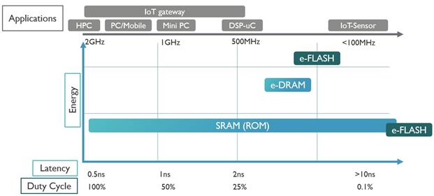
FIGURE 1. Application and performance space of the existing conventional memories (HPC = high performance computing; DSP = digital signal processing; ROM = read only memory; duty cycle = the proportion of time during which the memory device is operated).

For half a century, Moore’s Law has driven cost improvement of memory technologies, and this has translated into a continuous increase of the memory density. However, despite large improvements in memory density, only storage density (Flash NAND devices and tapes) has truly kept pace with the data growth rate. With the transition from NAND to 3D-NAND devices, density improvement for this storage class is however expected to slow down as well, and go below the data growth rate soon.

Unlike in logic development – which has always been driven by improvements in cost and device physics – improving the power/performing benefits for memory has barely been taken care of. As a result, energy reduction and speed improvement are far from following up the data growth rate, for both memory and storage devices (FIGURE 2).

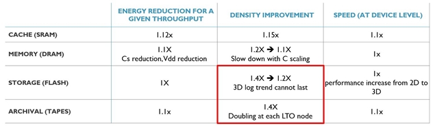
FIGURE 2. Growth rates for the main memory roadmaps; (red) only storage density has kept pace with the data growth rate.

Emerging technologies to the rescue?

To meet the memory requirements of the zettabyte era (i.e., improved density and speed, and reduced energy consumption), imec is exploring multiple emerging memory options, for standalone as well as for embedded applications (FIGURE 3). Options range from MRAM technologies for cache level applications, new ways for improving DRAM devices, emerging storage class memories to fill the gap between DRAM and NAND technologies, solutions for improving 3D-NAND storage devices, and a revolutionary solution for archival type of applications. Below, we review their status and challenges, and investigate whether these emerging memory roadmaps can cope with the zettabyte world.

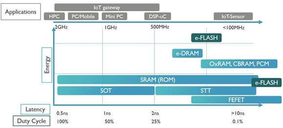
FIGURE 3. Memory research landscape at imec – application and performance space.

MRAM technologies for embedded cache level applications

Spin transfer torque MRAM (STT-MRAM) technology has emerged as a candidate technology for replacing L3 cache embedded SRAM memories. It offers non-volatility, high density, high speed and low switching current. The core element of an STT-MRAM device is a magnetic tunnel junction in which a thin dielectric layer is sandwiched between a magnetic fixed layer and a magnetic free layer. Writing of the memory cell is performed by switching the magnetization for the free magnetic layer, by means of a current that is injected perpendicular into the magnetic tunnel junction.

Because of this geometry, the read and write operations are performed through the same path, and this challenges the reliability of the device. These reliability issues in combination with increased energy at sub-ns switching speeds make STT-MRAM memories unsuitable for replacing the faster L1/L2 cache SRAM memories.

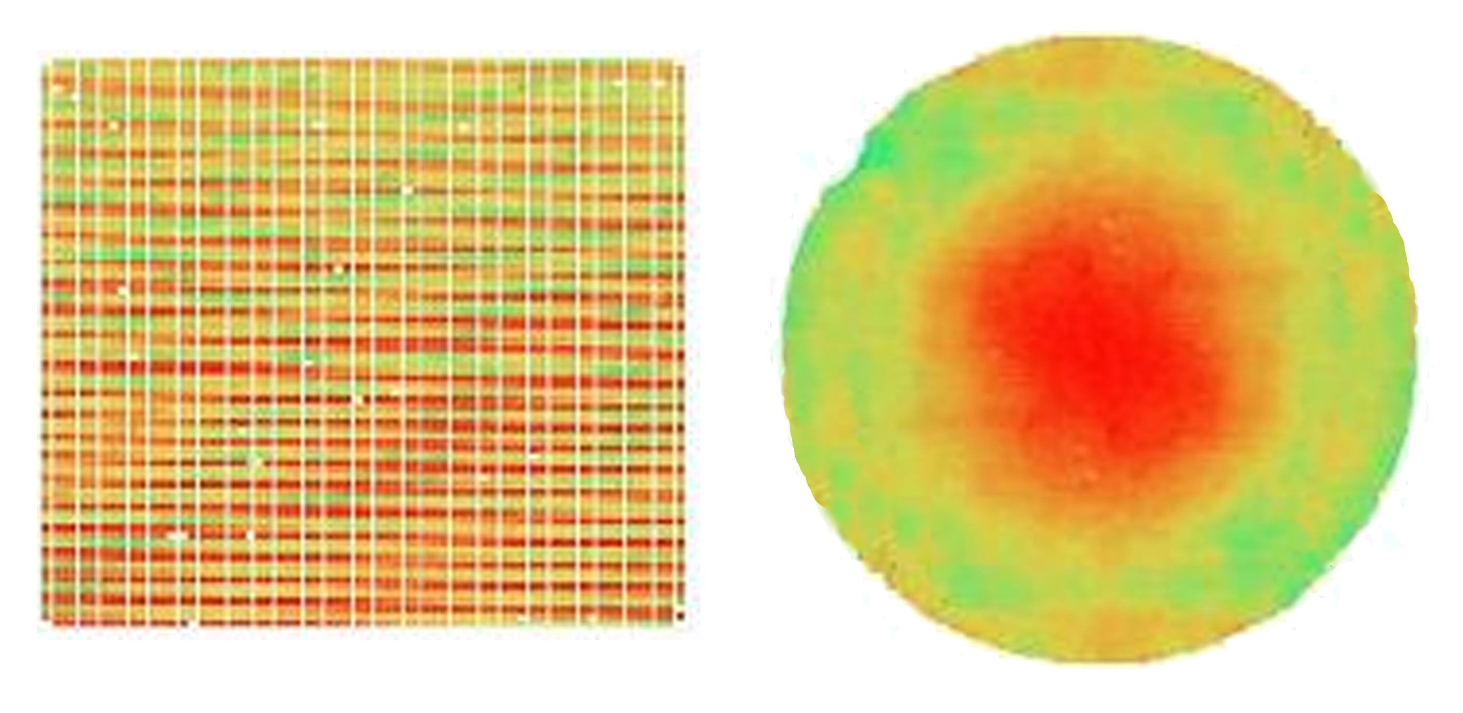
An MRAM variant, the spin orbit torque MRAM (SOT-MRAM), can overcome these issues. In these devices, switching the free magnetic layer is done by injecting an in-plane current in an adjacent SOT layer, as such de-coupling the read and write path and improving the device endurance and stability. Imec recently demonstrated the ability to fabricate state-of-the-art SOT-MRAM devices on 300mm wafers using CMOS compatible processes (FIGURE 4). The devices exhibited an unlimited endurance (>5×10¹⁰), fast switching speed (240ps), and power consumption as low as 300pJ. We also explore ways for further reducing energy consumption, by bringing down switching current and demonstrating field-free switching.

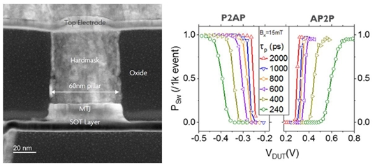
FIGURE 4. (Left) SOT-MRAM device, and (right) SOT switching distribution as a function of pulse voltage for various pulse lengths.

An imec view on DRAM scaling

DRAM is structurally a very simple type of memory. A DRAM memory cell consists of one transistor and one capacitor, that can be either charged or discharged. Traditionally, double-sided cylindrical capacitor structures have been used, with a dielectric material contained inside as well as outside the capacitor structure. However, when spacing becomes smaller, we need to increase the aspect ratio of these structures – since a certain amount of capacitor area is needed to maintain the memory’s performance. For very large aspect ratios, these DRAM structures are fabricated at the limits of mechanical stability. The industry may therefore transition to a new capacitor architecture: the high-aspect ratio one-pillar architecture, with the dielectric film now only on the outside (FIGURE 5). This change may make it possible to use thicker films of higher-k dielectrics, which in turn will allow reducing the aspect ratio of the one-pillar structure and improving leakage. A new dielectric with these specifications is currently under development at imec.

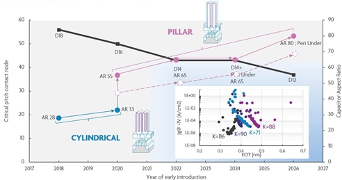
FIGURE 5. An imec view on the DRAM scaling roadmap; inset: impact of the one-pillar capacitor architecture

Further down the road, we are investigating if we can place the peripherical logic directly under the array of capacitors and transistors. This logic circuitry controls how data is moved to and from the memory chip, and typically consumes considerable area. Today, the transistor of the DRAM memory cell is however built on silicon. To be able to move the peri logic underneath the DRAM array, we need to replace this transistor with a non-Si transistor that is back-end compatible. At imec, we are moving towards a thin-film indium gallium zinc oxide (IGZO)-based transistor (FIGURE 6). This architecture is expected to give us one generation of Moore’s law scaling. In addition, it will enable ultimate 3D DRAM integration as well.

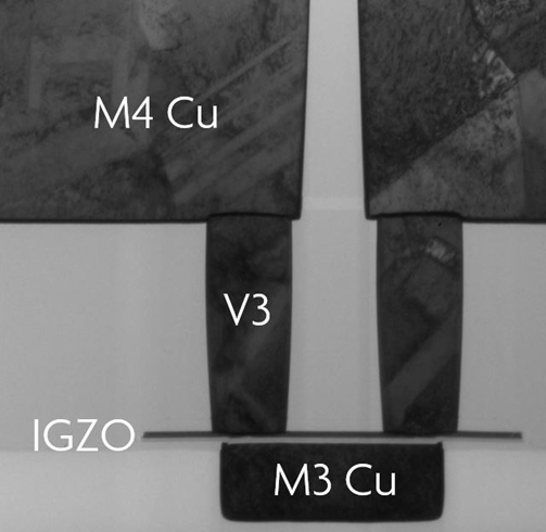
FIGURE 6. Novel oxide semiconductor based DRAM cell transistor.

Emerging memory and selector concepts for storage class memory

Storage class memory has been introduced to fill the gap between DRAM and NAND Flash memories in terms of latency, density, cost and performance. This new memory class should allow massive amounts of data to be accessed in a very short time. Most probably, more than one novel memory technology will be required to span the entire gap. The imec team explores several emerging technologies for storage class memory, including various cross-point-based architectures for the memory element, such as phase-change-RAM (PC-RAM), vacancy-modulated conductive oxide (VMCO), conductive bridging RAM (CB-RAM) and oxide RAM (OxRAM). When it comes to high-density applications, all these memory elements require two-terminal selector elements that connect serially with each of the memory elements. These selector elements suppress the sneak currents that run through the unselected cells in the cross-point array during memory operation. Imec is developing GeSe-based ovonic threshold switching (OTS) selector devices that fulfill the requirements imposed by high-density storage class memories, including high thermal and electrical stability, high current density and low off-state current.

Close to the DRAM side of the DRAM-NAND gap, high-density, high-speed MRAM offers an interesting, scalable alternative for the memory element. As this technology requires a selector as well, imec is working on a diode-based selector for this type of device. And finally, closer to the NAND Flash side, a ferroelectric memory based on hafnium-oxide (HfO) has gained interest. Compared to NAND-Flash, this emerging memory can operate at lower voltages and is much faster (with speeds down to 100ns). The easy cell structure can be fabricated with CMOS compatible processes and can be built in a 3D architecture.

3D NAND… and beyond?

Since its introduction several years ago, 3D NAND has become a mainstream storage technology because of its ability to significantly increase bit density. This is enabled by transitioning from 3 bits per cell to 4 bits per cell. And, instead of traditional x-y scaling in a horizontal plane, 3D NAND scales in the z direction by stacking multiple layers of NAND gates vertically. Today, stacking over 60 layers has become possible. However, increasing the numbers of layers challenges the deposition and etch processes. Also, the more layers that are stacked, the more stress evolves inside the layers, and this can cause a collapse of the 3D NAND pattern – a challenge that is tackled by imec. Imec also investigates alternative channel materials and processes – such as a silicon macaroni channel – that can overcome the limitations of the traditionally used poly-Si channels.

Despite all these advances, the density improvement of 3D NAND is expected to slow down and go below data growth rate soon. Therefore, the search for an emerging memory technology that is faster and cheaper than 3D NAND is ongoing. So far, there are no good candidates out there that can beat the 3D NAND density, especially because of the outstanding capability of 3D NAND Flash technology to integrate 3-4 bits per cell.

DNA storage: the holy grail of archival storage?

Imagine that we could store all data of the world in a container the size of a car, and store them for a very long time? That is exactly what DNA storage promises. DNA can be kept stable for millions of years – today, it is still possible to extract DNA from the woolly mammoth – guaranteeing long term retention. DNA as a medium for storage is also extremely dense and compact. Writing can be performed by encoding binary data onto strands of DNA through the process of DNA synthesis. The DNA strand can be built up with the base pairs representing a specific letter sequence, through a series of deprotection and protection reactions. As from the read side, there is an enormous technology push to sequence DNA faster and faster and at lower cost. Progress in DNA sequencing has been amazing, even outpacing Moore’s law. But researchers still have a long way to go before reasonable targets (1Gb/s) can be reached. To realize this, faster fluidics, faster chemical reactions and much higher parallelism are needed than what’s possible today. At imec, we work towards faster write/read operation, and towards making DNA storage a cost-effective solution for long-term storage.

Towards a sustainable zettabyte era

It has become clear that the classical memory roadmap cannot handle the zettabyte world in terms of energy, density, speed and cost. As shown above, imec is working on several emerging memory and storage technologies that can largely improve on density, system performance, and, partly, speed. However, energy consumption remains the biggest challenge towards a truly sustainable zettabyte era. And this highlights the need to continue collaborating with academia and industry on reduced energy consumption for memory technologies.

Talking about sustainability brings another aspect of the zettabyte era to mind: recycling. To be able to process and store all the data, massive amounts of devices will be produced. The advent of emerging technologies will also bring in new materials, which today are hardly recycled. To enable a truly sustainable zettabyte era, the semiconductor industry should therefore also find ways to improve the recyclability of all these materials.

GOURI SANKAR KAR is distinguished member technical staff emerging memories, and ARNAUD FURNEMONT is memory director at imec, Leuven, Belgium.

Editor’s Note: This article was originally published in the October 2018 issue of Solid State Technology. 

Tom Ho and Stewart Chalmers, BISTel, Santa Clara, CA

Traditional FDC systems collect data from production equipment, summarize it, and compare it to control limits that were previously set up by engineers. Software alarms are triggered when any of the summarized data fall outside of the control limits. While this method has been effective and widely deployed, it does create a few challenges for the engineers:

  • The use of summary data means that (1) subtle changes in the process may not be noticed and (2) the unmonitored section of the process will be overlooked by a typical FDC system. These subtle changes or the missed anomalies in unmonitored section may result in critical problems.
  • Modeling control limits for fault detection is a manual process, prone to human error and process drift. With hundreds of thousandssensors in a complex manufacturing process, the task of modeling control limits is extremely time consuming and requires a deep understanding of the particular manufacturing process on the part of the engineer. Non-optimized control limits result in misdetection: false alarms or missed alarms.
  • As equipment ages, processes change. Meticulously set control limit ranges must be adjusted, requiring engineers to constantly monitor equipment and sensor data to avoid false alarms or missed real alarm.

Full sensor trace detection

A new approach, Dynamic Fault Detection (DFD) was developed to address the shortcomings of traditional FDC systems and save both production time and engineer time. DFD takes advantage of the full trace from each and every sensor to detect any issues during a manufacturing process. By analyzing each trace in its entirety, and running them through intelligent software, the system is able to comprehensively identify potential issues and errors as they occur. As the Adaptive Intelligence behind Dynamic Fault Detection learns each unique production environment, it will be able to identify process anomalies in real time without the need for manual adjustment from engineers. Great savings can be realized by early detection, increased engineer productivity, and containment of malfunctions.

DFD’s strength is its ability to analyze full trace data. As shown in FIGURE 1, there are many subtle details on a trace, such as spikes, shifts, and ramp rate changes, which are typically ignored or go undetected by a traditional FDC systems, because they only examine a segment of the trace- summary data. By analyzing the full trace using DFD, these details can easily be identified to provide a more thorough analysis than ever before.

Dynamic referencing

Unlike traditional FDC deployments, DFD does not require control limit modeling. The novel solution adapts machine learning techniques to take advantage of neighboring traces as references, so control limits are dynamically defined in real time.  Not only does this substantially reduce set up and deployment time of a fault detection system, it also eliminates the need for an engineer to continuously maintain the model. Since the analysis is done in real time, the model evolves and adapts to any process shifts as new reference traces are added.

DFD has multiple reference configurations available for engineers to choose from to fine tune detection accuracy. For example, DFD can 1) use traces within a wafer lot as reference, 2) use traces from the last N wafers as reference, 3) use “golden” traces as reference, or 4) a combination of the above.

As more sensors are added to the Internet of Things network of a production plant, DFD can integrate their data into its decision-making process.

Optimized alarming

Thousands of process alarms inundate engineers each day, only a small percentage of which are valid. In today’s FDC systems, one of the main causes for false alarms is improperly configured Statistical Process Control (SPC) limits. Also, typical FDC may generate one alarm for each limit violation resulting in many alarms for each wafer process. DFD implementations require no control limits, greatly reducing the potential for false alarms.  In addition, DFD is designed to only issues one alarm per wafer, further streamlining the alarming system and providing better focus for the engineers.

Dynamic fault detection use cases

The following examples illustrate actual use cases to show the benefits of utilizing DFD for fault detection.

Use case #1End Point Abnormal Etching

In this example, both the upper and lower control limits in SPC were not set at the optimum levels, preventing the traditional FDC system from detecting several abnormally etched wafers (FIGURE 2).  No SPC alarms were issued to notify the engineer.

On the other hand, DFD full trace comparison easily detects the abnormality by comparing to neighboring traces (FIGURE 3).  This was accomplished without having to set up any control limits.

Use case #2 – Resist Bake Plate Temperature

The SPC chart in Figure 4 clearly shows that the Resist bake plate temperature pattern changed significantly; however, since the temperature range during the process never exceeded the control limits, SPC did not issue any alarms.

When the same parameter was analyzed using DFD, the temperature profile abnormality was easily identified, and the software notified an engineer (FIGURE 5).

Use case #3 – Full Trace Coverage

Engineers select only a segment of sensor trace data to monitor because setting up SPC limits is so arduous. In this specific case, the SPC system was set up to monitor only the He_Flow parameter in recipe step 3 and step 4.  Since no unusual events occurred during those steps in the process, no SPC alarms were triggered.

However, in that same production run, a DFD alarm was issued for one of the wafers. Upon examination of the trace summary chart shown in FIGURE 6, it is clear that while the parameter behaved normally during recipe step 3 and step 4, there was a noticeable issue from one of the wafers during recipe step 1 and step 2.  The trace in red represents the offending trace versus the rest of the (normal) population in blue. DFD full trace analysis caught the abnormality.

Use case #4 – DFD Alarm Accuracy

When setting up SPC limits in a conventional FDC system, the method of calculation taken by an engineer can yield vastly different results. In this example, the engineer used multiple SPC approaches to monitor parameter Match_LoadCap in an etcher. When the control limits were set using Standard Deviation (FIGURE 7), a large number of false alarms were triggered.   On the other hand, zero alarms were triggered using the Mean approach (FIGURE 8).

Using DFD full trace detection eliminates the discrepancy between calculation methods. In the above example, DFD was able to identify an issue with one of the wafers in recipe step 3 and trigger only one alarm.

Dynamic fault detection scope of use

DFD is designed to be used in production environments of many types, ranging from semiconductor manufacturing to automotive plants and everything in between. As long as the manufacturing equipment being monitored generates systematic and consistent trace patterns, such as gas flow, temperature, pressure, power etc., proper referencing can be established by the Adaptive Intelligence (AI) to identify abnormalities. Sensor traces from Process of Record (POR) runs may be used as starting references.

Conclusion

The DFD solution reduces risk in manufacturing by protecting against events that impact yield.  It also provides engineers with an innovative new tool that addresses several limitations of today’s traditional FDC systems.  As shown in TABLE 1, the solution greatly reduces the time required for deployment and maintenance, while providing a more thorough and accurate detection of issues.


TABLE 1
  FDC

(Per Recipe/Tool Type)

DFD

(Per Recipe/Tool Type)

FDC model creation 1 – 2 weeks < 1 day
FDC model validation and fine tuning 2 – 3 weeks < 1 week
Model Maintenance Ongoing Minimal
Typical Alarm Rate 100-500/chamber-day < 50/chamber-day
% Coverage of Number of Sensors 50-60% 100% as default
Trace Segment Coverage 20-40% 100%
Adaptive to Systematic Behavior Changes No Yes

TOM HO is President of BISTel America where he leads global product engineer and development efforts for BISTel.  [email protected].   STEWART CHALMERS is President & CEO of Hill + Kincaid, a technical marketing firm. [email protected].

Editor’s Note: This article was originally published in the October 2018 issue of Solid State Technology. 

PRASAD BACHIRAJU, Rudolph Technologies, Inc., Wilmington, Mass.

As IC manufacturers adopt advanced packaging processes and heterogeneous, multi-chip integration schemes to feed ever-greater consumer demand for more computing power in smaller and smaller spaces, their supply chains have become increasingly complex. A fab-wide view of the process, not so long ago the holy grail of yield management systems, now seems quaintly inadequate. Critical processes that affect finished product yields now occur in different facilities running diverse processes at locations spread around the world. A packaged electronics module may combine microprocessors, memory, MEMS sensors and RF communications, all from different fabs and each with its own particular history. Optimizing yields from such a complicated supply chain requires access to individual component genealogy that includes detailed knowledge of process events, equipment malfunctions and operational parameters, and much more. The latest generation of yield optimization systems consolidates this data – tool deep and supply-chain wide – in a monolithic database, providing end-to-end, die-level traceability, from bare wafer to final module test. Specialized algorithms, designed for “big data” but based on intimate knowledge of semiconductor manufacturing processes, can find hidden correlations among parameters, events and conditions that guide engineers to the root causes of yield losses and ultimately deliver increased fab productivity, higher process yields, and more reliable products.

Proactive Yield Perfection

Proactive yield perfection (PYP) is a comprehensive systems-level approach to perfecting yield through detailed surveillance and sophisticated modeling that identifies actual or potential root causes of excursions and establishes monitoring mechanisms to anticipate and proactively address problems before they result in yield loss. PYP is a logical extension of long-standing yield management practices that comprehends the dispersal and growing complexity of the manufacturing process and combines information from conventional defect detection, yield analysis, automated process control, and fault detection and classification techniques. It addresses two major obstacles identified within the industry: providing access to data across the fab and supply chain and integrating that data into device-level genealogy. PYP’s ability to correct small problems early is increasingly valuable in a complex supply chain where each step represents a considerable additional investment and a flawed finished module results in the costly loss of multiple component devices.

PYP collects data in a single database that integrates vital product parameter data from every die at each step in the process with performance and condition data from all tools, factories and providers in the supply chain. It provides unprecedented visibility of the entire manufacturing process from design, through wafer fab, test, assembly and packaging. Consolidating the data in a single, internally consistent database eliminates the considerable time often consumed in simply locating and aligning data stored in disparate databases at multiple facilities, and allows analytical routines to find correlations among widely separated observations that are otherwise invisible (FIGURE 1).

FIGURE 1. The PYP ecosystem

Genealogy incorporates traditional  device-level traceability of every die, but also provides access to all information available from sensors on the tool (temperature, pressure), process events (e.g. lot-to-lot changes and queue times), equipment events (e.g. alarms and preventive maintenance), changes in process configurations (e.g. specifications and recipes), and any other event or condition captured in the database for sophisticated analysis. Ready access to device genealogy allows analysts to trace back from failed devices to find commonalities that identify root causes, and trace forward from causes and events to find other device at risk of failure.

Mobile communications

A leading global supplier of mobile communications products has implemented the full PYP suite across their supply chain (FIGURE 2), which includes three separately located front-end fabs, a fabless design facility, oursourced manufacturing (foundries), and outsourced assembly and test (OSAT). Finished modules integrate data processing, data storage, RF communications, power management, analog sensing, and other functions using multiple die and components fabricated at various facilities around the world. The PYP suite comprises fault detection and classification, yield management, defect detection and classification, and run-to-run automated process control, including configurable dashboard displays that provide interactive drill-down reports and scheduled user-definable reports. The process flow includes front-end wafer-based processing, with singulated die then transferred to tape and subsequently to rectangular panels for back-end processing (FIGURE 3).

FIGURE 2. Numerous locations worldwide feed information into a single big-data cluster where multiple software solutions operate on the pre-aligned and internally consistent data set.

FIGURE 3. In a typical process flow, die move from wafer (front-end and back-end wafer fab), to reel, to panel, to final test and finally to the customer.

In one instance (FIGURE 4), panel mounted die were failing in back-end processing, causing yield losses valued at hundreds of thousands of dollars. The failed die were traced back to over a thousand wafers, and analysis of those wafers, using spatial pattern recognition, revealed defect clusters near the wafer edges. Further analysis of integrated MES (wafer process history) data traced the clusters to a defective tool that leaked etching solution onto wafers. Engineers are currently evaluating sensor data from the tool in an effort to identify a signal that will permit proactive intervention to prevent similar losses in the future.

FIGURE 4. A potential loss of hundreds of thousands of dollars due to final test on panel (left) was traced back to over a thousand wafers. Through yield analysis, an SPR pattern signaled wafers with edge defect clusters (center). Finally, the root cause is understood through MES analysis (right).

In another case, failed die on panels in the back-end showed a characteristic “strip” signature (FIGURE 5). Tracing the die backward revealed a front-end a process issue with the failing die all originating from locations near the center of the wafer.

FIGURE 5. The bad die (red strips) on the panel (left) were traced back the centers of the original wafers.

A final example from this manufacturer occurred in the back-end where die containing various filter technologies fabricated on a wafers of different sizes are combined on a panel substrate (FIGURE 6). In this case, the customer gained additional insights regarding the origin of the die being assembled and was able to evaluate how shifts in performance parameters impacted the final module product. This resulted in better matching of parts in the pre-assembly process and a tighter distribution of performance parameters in the outgoing modules.

FIGURE 6. A single panel contains different filter components from multiple (differently-sized) wafers. Die-level traceability allows engineers to relate final test results to inspection and metrology data collected during wafer processing. Die can be traced back to their individual location on the original wafer, permitting associations with location-specific data such as defect patterns discovered by SPR.

Automotive electronics

A leading global supplier of electronic systems to the automotive market manufactures finished modules containing multiple ICs from various suppliers and facilities. Highest reliability with component failure rates at parts-per-billion levels is an absolute requirement because the health and safety of millions of drivers may be jeopardized by a defective product. Limiting these risks, and the associated financial liability, through fast root-cause analysis of in-house test failures and field returns and rapid identification of process drift or step function changes are critical needs. Tuning the process to improve yields while preserving critical reliability is an equally important economic concern.

The final product is a multi-chip module containing microelectromechanical system (MEMS)-based sensors from one supplier and application-specific integrated circuits (ASIC) from another. These component parts are functionally tested prior to being send to an assembly facility where they are attached to a common carrier and packaged in a sealed module, which is then retested to verify functionality of the completed assembly. PYP software collects data across the entire supply chain. Devices from a single wafer lot are ultimately split and mixed among many modules. Using a commonality analysis, engineers can quickly identify die that share a similar risk and track them to their ultimate dispositions in finished modules. The tracking is not limited to wafer level. For instance, it might be used to find only those die located on the straight-line extension of a known crack or within at-risk regions identified by spatial pattern recognition (SPR). Such information is critical in issuing a recall of at-risk parts.

In this case, die that were known-good at wafer test were failing after assembly. Tracing back to wafer level the customer determined that all affected modules were assembled within a short time period of one another. Further investigation found that the packaging process was affecting peak-to-peak voltage at final test. The customer was not able to modify the assembly process, but they were able to eliminate the final test losses by tuning wafer probe specifications to eliminate die at risk for damage in the assembly operation. Die-level traceability across the supply chain, which allowed engineers to quickly and easily compare data sets on the same dies from wafer probe and final test, was key to achieving this solution.

Conclusion

Increasingly dispersed and complex supply chains require a proactive, integrated, systems-level approach to optimizing yields. PYP’s ability to integrate data – sensor-deep and supply chain-wide – in a monolithic database streamlines analysis and finds relationships that are otherwise invisible. Die-level genealogy allows engineers to trace die histories backward to find root causes of failures and forward to identify other die similarly at-risk. The value of PYP-based solutions is multiplied by the substantial investments made at each step of the process and the high cost and potential financial liability associated with failed, multi-chip modules.

PRASAD BACHIRAJU is Director, Customer Solutions, Rudolph Technologies, Inc., Wilmington, Mass.

Editor’s Note: This article was originally published in the October 2018 issue of Solid State Technology. 

By David W. Price, Douglas G. Sutherland, Jay Rathert, John McCormack and Barry Saville

Author’s Note:The Process Watch series explores key concepts about process control—defect inspection, metrology and data analytics—for the semiconductor industry. This article is the third in a series on process control strategies for automotive semiconductor devices. For this article, we are pleased to include insights from our colleagues at KLA-Tencor, John McCormack and Barry Saville. 

Semiconductors continue to grow in importance in the automotive supply chain, requiring IC manufacturers to adapt their processes to produce chips that meet automotive quality standards. The first article in this seriesfocused on the fact that the same types of IC manufacturing defects that cause yield loss also cause poor chip reliability and can lead to premature failures in the field. To achieve the high reliability required in automotive ICs, additional effort must be taken to ensure that sources of defects are eliminated in the manufacturing process. The second article in this seriesoutlined strategies, such as frequent tool monitoring and a continuous improvement program, that reduce the number of defects added at each step in the IC manufacturing process. This article explores how to drive tool monitoring to a higher level of performance in order to help automotive IC manufacturers achieve chip failure rates below the parts per billion level.

As a reminder, tool monitoring is the established best practice for isolating the source of random defectivity contributed by the fab’s process tools. During tool monitoring, a bare wafer is inspected to establish its baseline defectivity, run through a specific process tool (or chamber), and then inspected again. Any defects that were added to the wafer must have come from that specific process tool. This method can reveal the cleanest “golden” tools in the fab, as well as the “dog” tools that contribute the most defects and require corrective action. With plots of historical defect data from the process tools, goals and milestones for continuous improvement can be implemented.

When semiconductor fabs design their tool monitoring strategy, they must decide on the minimum size of defects that they want to detect and monitor. If historical test results have shown that smaller defects do not impact yield, then fabs will run their inspection tools at a lower sensitivity so that they no longer detect these smaller defects. By doing this, they can focus only on the larger yield-killer defects, avoiding distraction from the smaller “nuisance” defects. This approach works for a consumer fab that is only trying to optimize yield, but what about the automotive fab? Recall that yield and reliability issues are caused by the same defects types – yield and reliability defects differ only in their size and/or where they land on the device pattern.2 Therefore, a tool monitoring strategy that leaves the fab blind to smaller defects may be missing the very defects that will be responsible for future reliability issues.

Moreover, it’s important to understand that defects that seem small and inconsequential at one process layer may have a dramatic impact later in the process flow – their impact can be exacerbated by the subsequent process steps. The two SEM images in figure 1 were taken at exactly the same location on the same wafer, but at different steps of the manufacturing process. The image on the left shows a single, small defect that was found on the wafer after a deposition layer. This defect was previously thought to be a nuisance defect with no negative effect on the die pattern or chip performance. The image on the right shows that same deposition defect after metal 1 pattern formation. The presumed nuisance defect has altered the quality of the metal line printed several process steps later. This chip might pass electrical wafer sort, but this type of metal deformity could easily become a reliability issue in the field when activated by automotive environmental stressors.

Figure 1. The left image shows small particle created at a deposition layer. The right image shows the exact same location on the wafer after the metal 1 pattern formation. The metal line defect was caused by the small particle at the prior deposition layer. This type of deformity in the metal line could easily become a reliability issue in the field.

So how does an automotive IC fab determine the smallest defect size that will pose a reliability risk? To start, it is important to understand the impact of different defect sizes on reliability. Consider, for example, the different magnitudes of a line open defect shown in figure 2. A chip that has a pattern structure with a full line open will likely fail at electrical wafer sort and thus does not pose any reliability risk. A chip with a 50% line open – a line that is pinched or otherwise restricted to ~50% of its cross-sectional area – will likely pass electrical wafer sort but poses a significant reliability risk in the field. If this chip is used in a car, environmental conditions such as heat, humidity and vibrations, can cause degradation of this defect to a full line open, resulting in chip failure.

Figure 2. The image on the left shows a full line open, while the right image shows a ~50% line open. The chip on the left will fail at sort (assuming there is no redundancy). The chip on the right may pass electrical wafer sort but is a reliability risk in the field.

As a next step, it is important to understand how different size defects affect a chip’s pattern integrity. More specifically, what is the smallest defect that will result in a line open? What is the smallest defect that will result in a 50% line open?

Figure 3 shows the results of a Monte Carlo simulation that models the impact of different size defects introduced at a BEOL film deposition step. Minimum defect size is plotted on the vertical axis against varying metal layer pitch dimensions. This data corresponds to the metal 1 spacing for the 7nm, 10nm, 14nm and 28nm design nodes, respectively.

The green data points correspond to the smallest defects that will cause a full line open and the orange data points correspond to the smallest defects that will produce a 50% line open (i.e., a potential reliability failure). In each case the smallest defect that will cause a potential reliability failure is 50-75% of the smallest defect that will cause a full line open.

Figure 3. The green data points show the minimum defect size required to cause a full line open at the minimum metal pitch. The orange data points show the minimum defect size needed to cause a 50% line open. The x-axis is the metal 1 spacing for the 7nm (far left data point), 10nm, 14nm and 28nm (far right data point) design nodes.

These modeling results imply that to control for, and reduce, the number of reliability defects present in the process, fabs need to capture smaller defects. Therefore, they require higher sensitivity inspections than what is required for yield optimization. In general, detection of reliability defects requires an inspection sensitivity that is one node ahead of the current design node plan for yield alone. Simply put, a fab’s previous standards for reducing defectivity to optimize yield will not be sufficient to optimize reliability.

Increasing the sensitivities of the tool monitoring inspection recipes, or in some cases, using a more capable inspection system, will find smaller defects and possibly reveal previously hidden signatures of defectivity, as in Figure 4 below. While these signatures may have had a tolerable impact on yield in a consumer fab, they represent an unacceptable risk to reliability for automotive fabs pursuing continuous improvement and Zero Defect standards.

Figure 4: Hidden defect signatures that may impact reliability are often revealed with appropriate tool monitoring sensitivity. Zero Defect standards require corrective action on the process tool contributing these defects.

There are several important unpatterned wafer defect inspection factors for a fab to consider when creating a strategy to improve tool monitoring inspection sensitivity to find the small, reliability-related defects contributed by process tools. First, it is important to recognize that in a mature fab where yields are already high, there is rarely a single process layer or module that will be the “silver bullet” to reducing defectivity adequately to meet reliability improvement goals. Rather, it is sum of small gains across many layers that produce the desired gains in reliability. Because yield and the associated reliability improvements are cumulative across layers, reliability gains achieved through process tool monitoring using unpatterned wafer inspection are best demonstrated using a multi-layer regression model:

Yield = f(Ys)+f(SFS1)+f(SFS2)+ f(SFS3)+ ….. f(SFSN) + error

  • Ys = systematic yield loss (not particles related)
  • SFSx = cumulative Sursfcan unpatterned wafer inspection detected particles for many layers
  • Error = Yield loss mechanisms not detected by Surfscan

This implies that reliability improvements require a fab’s commitment to continuous improvement in defectivity levels across all processes and process modules.

Second, the fab should consider the quality of the bare wafer used for process tool monitoring. Recycling bare wafers increases the surface roughness with each cycle, an attribute known as haze. This haze level is fundamentally noise that affects the inspection system’s ability to differentiate the signal of smaller defects. Variability in haze across the population of test wafers acts as a limit to overall inspection recipe capability, requiring normalization, calibration and haze limits to reduce the impact of this noise source on defect sensitivity.

Next, the fab should ensure that the monitor step closely mimics the process that a production, patterned wafer follows. Small time-saving deviations in the monitor wafer flow to short cut the process may inadvertently skip the causal mechanism of defectivity. Furthermore, an over-reliance on mechanical handling checks alone bypasses the process completely and misses the critical contribution the process plays in particle generation.

When increasing the inspection recipe sensitivity, the fab must co-optimize both the “pre” and “post” inspection together. Often cycling the bare wafer through a process step can “decorate” small pre-existing defects on the wafer that were initially below the detection threshold. Once decorated, the defects now appear bigger and are more easily detected. In an unoptimized “post” inspection, these decorated defects can look like “adders,” leading to a false alarm and inadvertent process tool down time. Optimizing the inspections together maximizes the sensitivity and increases the confidence in the excursion alarms while avoiding time-consuming false alarms.

Lastly, it is important to review and classify the defects found during unpatterned inspection to correlate their relevance to the defects found at the equivalent patterned wafer process step. Only then can the fab be confident that the source of the defects has been isolated and appropriate corrective action has been taken.

To meet the high reliability demands of the automotive industry, IC manufacturers will need to go beyond simply monitoring and controlling the number of yield limiting defects on the wafer. They will need to improve the sensitivity of their tool monitoring inspections to one node smaller than what would historically be considered relevant. Only with this extra sensitivity can they detect and eliminate defects that would otherwise escape the fab and cause premature reliability failures. Additionally, when implementing a tool monitoring strategy, fabs need to carefully consider multiple factors, such as monitor wafer recycling, pre and post inspection sensitivity and the importance of a fab-wide continuous improvement program. With so much riding on automotive semiconductor reliability, increased sensitivity to smaller defects is an essential part of an optimal Zero Defect continuous improvement program.

About the Authors:

Dr. David W. Price and Jay Rathert are Senior Directors at KLA-Tencor Corp. Dr. Douglas Sutherland is a Principal Scientist at KLA-Tencor Corp. Over the last 15 years, they have worked directly with over 50 semiconductor IC manufacturers to help them optimize their overall process control strategy for a variety of specific markets, including implementation of strategies for automotive reliability, legacy fab cost and risk optimization, and advanced design rule time-to-market. The Process Watch series of articles attempts to summarize some of the universal lessons they have observed through these engagements.

John McCormack is a Senior Director at KLA-Tencor. Barry Saville is Consulting Engineer at KLA-Tencor. John and Barry both have over 25 years of experience in yield improvement and defectivity reduction, working with many IC manufacturers around the world.

References:

  1. Price, Sutherland and Rathert, “Process Watch: The (Automotive) Problem With Semiconductors,” Solid State Technology, January 2018.
  2. Price, Sutherland and Rathert, “Process Watch: Baseline Yield Predicts Baseline Reliability,” Solid State Technology, March 2018.

A lithographic method for TSV alignment to embedded targets was evaluated using in-line stepper self metrology, with TIS correction.

BY WARREN W. FLACK, Veeco Instruments, Plainview, NY and JOHN SLABBEKOORN, imec, Leuven, Belgium

Demand for consumer product related devices including backside illuminated image sensors, interposers and 3D memory is driving advanced packaging using through silicon via (TSV) [1]. The various process flows for TSV processing (via first, via middle and via last) affect the relative levels of integration required at the foundry and OSAT manufacturing locations. Via last provides distinct advantages for process integration, including minimizing the impact on back end of line (BEOL) processing, and does not require a TSV reveal for the wafer thinning process. Scaling the diameter of the TSV significantly improves the system performance and cost. Current via last diameters are approximately 30μm with advanced TSV designs at 5 μm [2].

Lithography is one of the critical factors affecting overall device performance and yield for via last TSV fabrication [2]. One of the unique lithography requirements for via last patterning is the need for back-to-front side wafer alignment. With smaller TSV diameters, the back-to- front overlay becomes a critical parameter because via landing pads on the first level metal must be large enough to include both TSV critical dimension (CD) and overlay variations, as shown in FIGURE 1. Reducing the size of via landing pads provide significant advantages for device design and final chip size. This study evaluates 5μm TSVs with overlay performance of ≤ 750nm.

Alignment, illumination and metrology

Lithography was performed using an advanced packaging 1X stepper with a 0.16 numerical aperture (NA) Wynne Dyson lens. This stepper has a dual side alignment (DSA) system which uses infrared (IR) illumination to view metal targets through a thinned silicon wafer [3]. For the purposes of this study and its results, the wafer device side is referred to as the “front side” and the silicon side is referred to as the “back side.” The side facing up on the lithography tool is the back side of the TSV wafer, as shown in FIGURE 2.

The top IR illumination method for viewing embedded alignment targets, shown in Fig. 2, provides practical advantages for integration with stepper lithography. Since the illumination and imaging are directed from the top, this method does not interfere with the design of the wafer chuck, and does not constrain alignment target positioning on the wafer. The top IR alignment method illuminates the alignment target from the back side using an IR wavelength capable of transmitting through silicon (shown as light green in FIGURE 2) and the process films (shown in blue). In this configuration the target (shown in orange) needs to be made from an IR reflective material such as metal for optimal contrast. The alignment sequence requires that the wafer move in the Z axis in order to shift alignment focus from the wafer surface to the embedded target.

Back-to-front side registration was measured using a metrology package on the lithography tool which uses the DSA alignment system. This stepper self metrology package (DSA-SSM) includes routines to diagnose and compensate for measurement error from having features at different heights. For each measurement site the optical metrology system needs to move the focus in Z between the resist feature and the embedded feature. Therefore angular differences between the Z axis of motion, the optical axis of the alignment camera, and the wafer normal will contribute to measurement error for the tool [3]. The quality of the wafer stage motion is also very important because a significant pitch and roll signature would result in a location dependent error for embedded feature measurement, which would complicate the analysis.

If the measurement operation is repeatable and consistent across the wafer, then a constant error coming from the measurement tool, commonly referred to as tool induced shift (TIS), can be characterized using the method of TIS calibration, which incorporates measurements at 0 and 180 degree orientations. The TIS error—or calibration—is calculated by dividing the sum of offsets for the two orientations by two [4]. While the TIS calibration is effective for many types of measurements for planar metrology, for embedded feature metrology, the quality of measurement and calibration also depend on the quality and repeatability of wafer positioning, including tilt. In previous studies, the registration data obtained from the current method were self consistent and proved to be an effective inspection method [3, 5]. However given the dependencies affecting TIS calibration for embedded feature metrology, it is desirable to confirm the registration result using an alternate metrology method [5]. In order to independently verify the DSA-SSM, overlay data dedicated electrical structures were designed and placed on the test chip.

Electrical verification of TSV alignment is performed after complete processing of the test chip and relies on the landing position of a TSV on a fork-to-fork test structure in the embedded metal 1 (damascene metal). When the TSV processing is complete the copper filled TSV will make contact with metal 1. The TSV creates a short between the two sets of metal forks, allowing measurement of two resistance values which can be translated into edge measurements. For the case of ideal TSV alignment, the two resistances are equal. The measurement resolution of the electrical structure is limited by the pitch of the fork branches. In this study resolution is enhanced by creating structures with four different fork pitches. A similar fork-to-fork structure rotated 90 degrees is used for the Y alignment. Using this approach both overlay error and size of the TSV in both X and Y can be electrically determined [6].

Experimental methods

This study scrutinizes image placement performance by examining DSA optical metrology repeatability after TSV lithography, and then comparing this optical registration data with final electrical registration data.

The TSV-last process begins with a 300mm device wafer with metal 1, temporarily bonded to a carrier for mechanical support as shown in FIGURE 3. The back side of the silicon device wafer (light green) is thinned by grinding and then polished smooth by chemical mechanical planarization (CMP). The TSV is imaged in photoresist (red) and etched through the thinned silicon layer. FIGURE 3 depicts the complete process flow including the TSV, STI and PMD etch, TSV fill, redis- tribution layer (RDL) and de-bonding from carrier. The aligned TSV structure must land completely on the metal 1 pad (dark blue).

TSV lithography is done with a stepper equipped with DSA. The photoresist is a gh-line novolac based positive- tone material requiring 1250mJ/cm2 exposure dose with a thickness of 7.5μm [5]. The TSV diameter is 5μm, and the silicon thickness is 50μm. TSV etching of the silicon is performed by Bosch etching [7]. Tight control of lithography and TSV etching is required to insure that vias land completely on metal 1 pads, as shown in FIGURE 1.

Acceptable features for DSA-SSM metrology need to fit the via process requirements for integration. Since the TSV etch process is very sensitive to pattern size and density, the TSV layer is restricted to one size of via, and the DSA-SSM measurement structure is constructed using this shape. The design of the DSA-SSM measurement structure uses a cluster of 5μm vias with unique grouping and clocked rotation to avoid confusion with adjacent TSV device patterns during alignment.

FIGURE 4 shows two different focus offsets of DSA camera images of the overlay structure. For this structure, the reference metal 1 feature (outlined by the blue ring) and the resist pattern feature (outlined by the red ring) are not in the same focal plane. For a silicon thickness of 50μm, focusing on one feature will render the other feature out of focus, requiring each feature to have its own focus offset, which is specified in the metrology measurement recipe.

Optical registration process control

This study leveraged a sampling plan of 23 lithography fields with 5 measurements per field, resulting in a total of 115 measurements per wafer. Since the full wafer layout contains 262 fields, this sampling plan provides a good statistical sample for monitoring linear grid and intrafield parameters.

In the initial run, the overlay settings were optimized using the DSA-SSM metrology feedback and then the parameters were fixed to investigate overlay stability over a nine-week period. Trend charts for mean and 3σ for seven TSV lots are shown in FIGURE 5. Each measurement lot consists of 8 wafers, with 115 measure- ments per wafer, and all data is corrected for TIS on a per lot basis using measurements of a single wafer at 0 and 180 degree orientations [3]. The lot 3σ is consistently less than 600nm over the nine-week period. There appears to be a consistent small Y mean error (blue diamond) that could be adjusted to improve subsequent overlay results. With a Y mean correction applied, the registration data shows mean plus 3σ ≤ 600nm.

Validating TSV alignment and in-line optical metrology

Two TSV last test chip wafers were completely processed to the stage that they can be electrically measured. TABLE 1 shows the registration numbers confirming a good match between the two metrology methods. It is important to note that an extra translation step is performed between the optical and the electrical measurement: the TSV etch.

In this analysis the TSV etch is assumed to be perfectly vertical. From the data we can conclude that the TSV etch is indeed vertical enough not to interfere with the overlay data. Otherwise this would show as translation or scaling effects between the two metrology methods.

Conclusions

The lithographic method for TSV alignment to embedded targets was evaluated using in-line stepper self metrology, with TIS correction. Registration data was collected over a nine-week period to characterize the stability of TSV alignment. With corrections applied, the registration data demonstrates mean plus 3σ ≤ 600nm. The in-line optical registration data was then correlated to detailed electrical measurements performed on the same wafers at the end of the process to provide independent assessment of the accuracy of the optical data. Good correlation between optical and electrical data confirms the accuracy of the in-line optical metrology method, and also confirms that the TSV etch through 50μm thick silicon is vertical.

References

1. Vardaman, J. et. al., TechSearch International: Advanced Packaging Update, July 2016.
2. Van Huylenbroeck, S. et. al., “Small Pitch High Aspect Ratio Via Last TSV Module”, The 66th Electronic Components and Technology Conference, Los Vegas, NV, May 2016.
3. Flack, W. et. al., “Optimization of Through Si Via Last Lithography for 3D Packaging”, Twelfth International Wafer- Level Packaging Conference, San Jose, CA, October 2015.
4. Preil, M. et. al, “Improving the Accuracy of Overlay Measurements through Reduction of Tool and Wafer Induced Shifts”, Metrology, Inspection, and Process Control for Microlithography Proceedings, SPIE 3050, 1997.
5. Flack, W. et. al., “Verification of Back-to-Front Side Alignment for Advanced Packaging”, Ninth Interna- tional Wafer-Level Packaging Conference, Santa Clara, CA, November. 2012.
6. Flack, W. et.al., “Overlay Performance of Through Si Via Last Lithography for 3D Packaging”, 18th Electronics Packaging Technology Conference, Singapore, December 2016
7. Slabbekoorn, J. et. al, “Bosch Process Characterization For Donut TSV’s” Eleventh International Wafer-Level Packaging Conference, Santa Clara, CA, November 2014.

Layout schema generation generates random, realistic, DRC-clean layout patterns of the new design technology for use in test vehicles.

BY WAEL ELMANHAWY and JOE KWAN, Mentor Graphics, Beaverton, OR

Predicting and improving yield in the early stages of technology development is one of the main reasons we create test macros on test masks. Identifying potential manufacturing failures during the early technology development phase lets design teams implement upstream corrective actions and/or process changes that reduce the time it takes to achieve the desired manufacturing yield in production. However, while conventional yield ramp techniques for a new technology node rely on using designs from previous technology nodes as a starting point to identify patterns for design of experiment (DoE) creation, what do you do in the case of a new design technology, such as multi- patterning, that did not exist in previous nodes? The human designer’s experience isn’t applicable, since there isn’t any knowledge about similar issues from previous designs. Neither is there any prior test data from which designers can draw feedback to create new test structures, or identify process or design style optimizations that can improve yield more quickly.

An innovative new technology, layout schema gener- ation (LSG), enables design teams to generate additional macros to add to test structures without relying on past designs for input. These macros are based on the gener- ation and random placement of unit patterns that can construct more meaningful larger patterns. Specifications governing the relationships between those unit patterns can be adjusted to generate layout clips that look like realistic designs. Those layout clips can then be used in design of experiment (DoE) trials to predict yield, and identify potential design and process optimizations that will help improve yield. By using this new LSG process, designers can significantly reduce the time it takes to achieve the desired yield for designs that include new design techniques.

Issues affecting yield

Wafer yield is typically reduced by three categories of defects. The first category comprises random defects, which occur due to the existence of contamination particles in the different process chambers. A conducting particle can short out two or more neighboring wires, or create a leakage path. A non-conducting particle or a void can open up a wire or a via, or create high resistive paths. FIGURE 1 shows scanning electron microscope (SEM) images of these two types of random defects.

The second category contains systematic defects, which occur due to an imperfect physical layout architecture, or the impact of non-optimized optical process recipes and/ or equipment. Systematic defects are typically the biggest source of yield detraction [1], but a majority of them can be eliminated through design-technology co-optimization (DTCO), in which the design and process sides commu- nicate more freely to achieve faster rates of improvement.

The third category, which we’re not addressing in this article, includes parametric defects (such as a lack of uniformity in the doping process) that may affect the reliability of devices.

Layout schema generation

To demonstrate the use and applicability of the LSG process, let’s look at designs that use the self-aligned multi-patterning (SAMP) process. Multi-patterning (MP) technology with ArF 193i lithography is currently the preferred choice over extreme ultraviolet (EUV) lithography for advanced technology nodes from 20nm on down. At 7 nm and 5 nm nodes, the SAMP process appears to be one of the most effective MP techniques in terms of achieving a small pitch of printed lines on the wafer, but its yield is in question. Of course, before being deployed in production, it must be thoroughly tested on test vehicles. However, without any previous SAMP designs, design of an appropriate test vehicle is challenging. In addition to the lack of historical test data, the unidirectional nature of the SAMP design complicates the design of the conven- tional serpentine and comb test shapes, which contain bidirectional components.

Self-aligned multi-patterning process

In the SAMP process [3], the first mask is known as the mandrel mask. Sacrificial mandrel shapes are printed with a relaxed pitch, and then used to develop sidewalls. The sidewalls are at half the mandrel’s pitch. Depending on the tone, target shapes may exist in the spaces between the sidewalls. The target shapes can be reused as sacrificial mandrel shapes to form another generation of sidewalls. Wafer shapes that don’t have corresponding mask shapes are called non-mandrel shapes. This process can be repeated to achieve SAMP layouts with a reduced pitch. The SAMP process (FIGURE 2) restricts the designs to be almost unidirectional. Generated parallel lines will be cut later by a cut mask at the desired line ends to form the correct connectivity.

Test vehicles

A test vehicle is typically a subset of the masks for a design, designed specifically to induce potential systematic failures or lithographic hotspots on the layer under test. It may also contain some test structures specially designed for the detection of random defects. The main compo- nents in a test vehicle for any new node are serpentine and comb shapes (to capture random defects), and preliminary standard cell designs (with many variations, to assess their quality). Other structures are typically added based on experience derived from production chips of previous nodes.

In a new node, all test structures on the test vehicle are vital for process training and characterization. Feedback from the test process is used for design style optimization. For example, when “bad” layout geometries are discovered after manufacturing, they can be captured as patterns, assigned low scores, and stored in a design for manufacturing (DFM) pattern library [2]. The designer can then use DFM analysis to find the worst patterns in a given layout, and modify or eliminate them. Such early DTCO provides a faster yield ramp for new nodes. Even in mature nodes, test structures are used on production wafers to identify additional opportunities for process refinement and optimization, which will have a positive impact on future yield.

One of the obstacles in test vehicle design is that it depends mainly on human designer’s experience and memory. Although experienced designers have seen multiple design styles in older nodes, the design shapes they are familiar with are limited to those styles. It typically takes a long time to design new test structures that cover new shapes, especially for a new process. The LSG solution adds more macros (generated in a random fashion) to the standard test structures strategy to speed up new shape yield analysis.

Random test pattern generation

The key component of the LSG solution is a method for the random generation of realistic design-like layouts, without design rule violations. The LSG process uses a Monte Carlo method to apply randomness in the generation of layout clips by inserting basic unit patterns in a grid. These unit patterns represent simple rectangular and square polygons, as well as a unit pattern for inserting spaces in the design. Unit pattern sizes depend on the technology pitch value. During the generation of the layouts, known design rules are applied as constraints for unit pattern insertion. Once the rules are configured, an arbitrary size of layout clips can be generated (FIGURE 3).

To begin, the SAMP design rules are converted to a format readable by an automated LSG tool like the Calibre® LSG tool from Mentor, a Siemens Business. Once the rules are configured, the Calibre LSG process can automatically generate an arbitrarily wide area of realistic DRC-clean SAMP patterns. The area is only limited by the floorplan of the designated macro of SAMP test structures. Test patterns can be also generated with power rails to mimic the layouts of standard cells. FIGURE 4 shows a sample clip of the generated output layout. To be ready for the experiments, the SAMP design is decomposed into the appropriate mandrel and cut masks, according to the decomposition rules. This operation also distinguishes between mandrel and non-mandrel shapes.

Design of Experiment

In the design phase of the test vehicle, the generated SAMP patterns are added to the typical contents of regular test patterns. The random SAMP patterns are electrically meaningless, unless they are connected to other layers to set up the required experiment. The DoE determines the way the connections are made from the patterns up to the testing pads, to detect different fail modes. Fail modes include short circuits due to lithographic bridging or conducting particles, and open circuits due to lithographic pinching, non-conducting particles, voids, or open vias.

A via chain can be constructed to connect the random DoE of SAMP structures through a routing layer to external pads for electrical measurement. These clips are decomposed according to the decomposition rules of the technology into the appropriate mandrel and cut masks. The decomposed clips can be tested through simulations, or electrically on silicon to discover hotspots. The discovered hotspots can be analyzed to determine root cause, which can be used to modify design layouts and/or optimize the fabrication process and models to eliminate these hotspots in future production. They can also be used as learning patterns for DFM rule deck devel- opment. By expanding the size of the randomly generated test structures, more hotspots can be detected, which can provide an even faster way to enhance the yield of a new technology node.

To demonstrate the effectiveness of the LSG process, we performed two experiments on a set of SAMP patterns similar to those shown in FIGURE 4.

Detecting random conducting particles

The first experiment collected data about random defects caused by conducting particles. In this experiment, all mandrel shapes are connected through the upper (or lower) via and metal layers, up to a testing pad. All non-mandrel shapes are connected in the same way to another testing pad. The upper routing layer forms two interdigitated comb shapes. FIGURE 5 shows a layout snippet of the connections. All via placements and upper metal routings were made with a custom script, without the intervention of a human designer. Ideally the two testing pads should be disconnected, as no mandrel shape can touch a non-mandrel shape. If the testing probes are found to be connected, this likely indicates a random conducting particle defect, or a lithographic bridge. The localization and analysis of such defects [4] can help with yield estimation and enhancement.

Detecting systematic cut mask resolution problems

One example of a systematic lithographic defect found in SAMP designs is when the cut mask is not resolved correctly. This causes two shapes on the same track to be shorted out through the unresolved cut shape. The testing of such a case requires connecting every other polygon on the same track. This was done with a generating script, without the intervention of human designers. FIGURE 6 shows a snippet of the generated layout with the connections. If the test probes are found to be connected while the two pads (ideally) are disconnected, this may indicate an unresolved cut shape. The analysis of the defect location and data from multiple wafers can prove the root cause of the defect.

Results

The two experiments described above were placed on a test vehicle of an advanced node. The test macro containing the first experiment setup successfully detected several conducting particle defects. A sample SEM image of the discovered defect is shown in FIGURE 7. Statistical data from multiple wafers were used to model the defect density and estimate the yield target.

Repetitive fail data from the test macro of the second experiment indicated systematic failures at particular locations. The analysis showed that the root cause of the failure was a poorly resolving cut shape in some process corners, as was predicted in the DoE. FIGURE 8 shows a snippet of the generated layout and its contour simulation.

To test the effectiveness of the random approach in capturing defects, 20 SAMP design clips were generated with linearly increasing sizes, such that the 20th clip was 20X bigger than the first clip. Lithography simulations were executed on the cut mask to inspect potential failures. The contours were checked, and potential failures were identified and categorized. FIGURE 9 shows the number of the unique hotspots found in each clip. The graph shows that the number of identified hotspots tends to saturate with the chip size. The second clip has 2X the number of unique hotspots found in the first clip, while the 20th clip only sees around a 6X increase. This result is expected, as many hotspots in the larger clips are just replicas of those found in the small clips. Assuming that the LSG tool is configured correctly, this result means most of the potential hotspots can be covered in a reasonable size test vehicle.

Conclusion

Test vehicles are vital for yield ramp up in new technologies and yield enhancement in mature nodes, but it can be difficult to design accurate test structures for new design styles and technologies that have no relevant history. Innovative techniques are needed to achieve comprehensive coverage of potential manufacturing failures created by new design styles, while ensuring full compliance with known design rule checks. A new solution using layout schema generation generates random, realistic, DRC-clean layout patterns of the new design technology for use in test vehicles. Experiments with this technology show it can provide high coverage of new design styles for an arbitrarily-wide design area. Circuitry can be added to the generated clips to make them electrically measurable for the detection of potential failures. The ability to discover lithographic hotspots and systematic failures early in the technology development process is significantly improved, at the expense of additional testing area. This design/technology co-optimization speeds up the yield optimization for new technology nodes, improving a critical success factor for market success.

References

1. Lee, J.H., Lee, J.W., Lee, N.I., Shen, X., Matsuhashi, H., Nehrer, W., “Proactive BEOL yield improvement methodology for a successful mobile product,” Proc. IEEE ISCDG, 93-95 (2012).
2. Park, J., Kim, N., Kang, J.-H., Paek, S.W., Kwon, S., Shafee, M., Madkour, K., Elmanhawy, W., Kwan, J., et al., “High coverage of litho hotspot detection by weak pattern scoring,” Proc. SPIE 9427, 942703 (2015)
3. Bencher, C., Chen, Y., Dai, H., Montgomery, W., Huli, L., “22nm half-pitch patterning by CVD spacer self alignment double patterning (SADP),” Proc. SPIE 6924, 69244E (2008)
4. Schmidt, M., Kang, H., Dworkin, L., Harris, K., Lee, S., “New methodology for ultra-fast detection and reduction of non-visual defects at the 90nm node and below using comprehensive e-test structure infrastructure and in-line DualBeamTM FIB,” IEEE/ SEMI ASMC, 12-16 (2006).

TechInsights (Ottawa, Canada), announced its new Power Semiconductor subscription, a technical intelligence service that provides regular, succinct analysis of emerging power semiconductor products as they enter mass production in high-volume applications. In addition, the company is offering custom analysis services for power semiconductor products.

“The semiconductor industry is developing smaller, more efficient power process technologies, using Silicon Carbide and Gallium Nitride,” said Mike McLean, SVP of Technology at TechInsights. “Our new Power Semiconductor subscription service is ideal for market leaders seeking to design roadmaps based on hard facts about cutting-edge Gallium Nitride, Silicon Carbide, and Silicon devices.”

The Power Semiconductor Subscription service includes:

  • 10 summary reports and hundreds of high-resolution supporting images
  • Analysis coverage including device metrics, package x-rays, die photos, SEM plan-view images and cross-sectional SEM images, cross-sectional TEM images and material analysis
  • TechInsights tri-annual analyst briefing
  • An annual patent landscape summary
  • Annual analyst workshop
  • Real time updates provide access to work in progress as well as exploratory work on more than 30 devices

TechInsights’ primary focus for the 2019 Power Semiconductor subscription is consumer applications of Gallium Nitride technology, specifically where it has the potential to replace super junction MOSFET devices in low form factor applications. Additionally, the company plans to monitor Silicon Carbide technologies as they compete with IGBT, and innovations in the mature Silicon technology that allow it to compete with Gallium Nitride and Silicon Carbide. The analysis will include technology and products from more than 20 major companies driving innovation using these technologies.

Source Photonics, a global provider of optical transceivers, today announced it recently closed more than $100M in equity to support its growing data center and 5G business.

The funding will be used to further increase the scale of Source Photonics’ operations, as LightCounting reported that the sales of optical components and modules to Cloud Companies grew by 63% in 2016 and 64% in 2017. The growth rate will average roughly 20% per year through 2023. Higher growth rates in 2020-2022 will be driven by first volume deployments of 400GbE. This is a result of the rise of 5G and the cloud.

Planned developments include the creation of a new laser fab, upgrades to existing production facilities and increased investment in the research and development of next-generation technologies, ensuring Source Photonics continues its position as a leading innovator.

“Exciting new applications such as the Internet of Things (IoT), Virtual Reality, and cloud services are growing in popularity every day,” said Doug Wright, CEO at Source Photonics. “These applications all depend on the next standard of connectivity, and 5G depends on the backing of a world-class optical network. We are extremely proud that our investors have shown this confidence in us and are confident that the investment will support our ongoing work to enable the next era of connectivity.”

Upgrades to Source Photonics’ fab in Taiwan have already been completed and production operations have begun for a new fab in Jintan, China, using the latest funding. The funding will also be used towards technology investments for advanced coating technologies to enable next-generation lasers and transceivers for the fast-growing 5G and data center markets.

Source Photonics’ latest range of cutting-edge technology will be exhibited at OFC 2019 at booth 4021. Products on display will include its new 400G-LR8 and DR4 QSFP-DD solutions, which are the latest addition to its PAM4-based optical transceivers portfolio. Other products which will be showcased at OFC, in San Diego, on March 4-7, 2019, include several QSFP28 solutions such as the 100G-DR/FR, 100G-SR4, 100G CWDM4, and 100G-LR4. The company will also demonstrate some of its solutions for the 5G market such as the 50G-ER QSFP28 and 25G LAN DWM SFP28.

Researchers at Tokyo Institute of Technology (Tokyo Tech) report a unipolar n-type transistor with a world-leading electron mobility performance of up to 7.16 cm2 V-1 s-1. This achievement heralds an exciting future for organic electronics, including the development of innovative flexible displays and wearable technologies.

Researchers worldwide are on the hunt for novel materials that can improve the performance of basic components required to develop organic electronics.

Now, a research team at Tokyo Tech’s Department of Materials Science and Engineering including Tsuyoshi Michinobu and Yang Wang report a way of increasing the electron mobility of semiconducting polymers, which have previously proven difficult to optimize. Their high-performance material achieves an electron mobility of 7.16 cm2 V-1 s-1, representing more than a 40 percent increase over previous comparable results.

In their study published in the Journal of the American Chemical Society, they focused on enhancing the performance of materials known as n-type semiconducting polymers. These n-type (negative) materials are electron dominant, in contrast to p-type (positive) materials that are hole dominant. “As negatively-charged radicals are intrinsically unstable compared to those that are positively charged, producing stable n-type semiconducting polymers has been a major challenge in organic electronics,” Michinobu explains.

The research therefore addresses both a fundamental challenge and a practical need. Wang notes that many organic solar cells, for example, are made from p-type semiconducting polymers and n-type fullerene derivatives. The drawback is that the latter are costly, difficult to synthesize and incompatible with flexible devices. “To overcome these disadvantages,” he says, “high-performance n-type semiconducting polymers are highly desired to advance research on all-polymer solar cells.”

The team’s method involved using a series of new poly(benzothiadiazole-naphthalenediimide) derivatives and fine-tuning the material’s backbone conformation. This was made possible by the introduction of vinylene bridges[1] capable of forming hydrogen bonds with neighboring fluorine and oxygen atoms. Introducing these vinylene bridges required a technical feat so as to optimize the reaction conditions.

Overall, the resultant material had an improved molecular packaging order and greater strength, which contributed to the increased electron mobility.

Using techniques such as grazing-incidence wide-angle X-ray scattering (GIWAXS), the researchers confirmed that they achieved an extremely short π-π stacking distance[2] of only 3.40 angstrom. “This value is among the shortest for high mobility organic semiconducting polymers,” says Michinobu.

There are several remaining challenges. “We need to further optimize the backbone structure,” he continues. “At the same time, side chain groups also play a significant role in determining the crystallinity and packing orientation of semiconducting polymers. We still have room for improvement.”

Wang points out that the lowest unoccupied molecular orbital (LUMO) levels were located at -3.8 to -3.9 eV for the reported polymers. “As deeper LUMO levels lead to faster and more stable electron transport, further designs that introduce sp2-N, fluorine and chlorine atoms, for example, could help achieve even deeper LUMO levels,” he says.

In future, the researchers will also aim to improve the air stability of n-channel transistors — a crucial issue for realizing practical applications that would include complementary metal-oxide-semiconductor (CMOS)-like logic circuits, all-polymer solar cells, organic photodetectors and organic thermoelectrics.

Zips on the nanoscale


February 28, 2019

Nanostructures based on carbon are promising materials for nanoelectronics. However, to be suitable, they would often need to be formed on non-metallic surfaces, which has been a challenge – up to now. Researchers at Friedrich-Alexander-Universität Erlangen-Nürnberg (FAU) have found a method of forming nanographenes on metal oxide surfaces. Their research, conducted within the framework of collaborative research centre 953 – Synthetic Carbon Allotropes funded by the German Research Foundation (DFG), has now been published in the journal Science.

Two-dimensional, flexible, tear-resistant, lightweight, and versatile are all properties that apply to graphene, which is often described as a miracle material. In addition, this carbon-based nanostructure has unique electrical properties that make it attractive for nanoelectronic applications. Depending on its size and shape, nanographene can be conductive or semi-conductive – properties that are essential for use in nanotransistors. Thanks to its good electrical and thermal conductivity, it could also replace copper (which is conductive) and silicon (which is semi-conductive) in future nanoprocessors.

New: Nanographene on metal oxides

The problem: In order to create an electronic circuit, the molecules of nanographene must be synthesised and assembled directly on an insulating or semi-conductive surface. Although metal oxides are the best materials for this purpose, in contrast to metal surfaces, direct synthesis of nanographenes on metal oxide surfaces is not possible as they are considerably less chemically reactive. The researchers would have to carry out the process at high temperatures, which would lead to several uncontrollable secondary reactions. A team of scientists led by Dr. Konstantin Amsharov from the Chair of Organic Chemistry II have now developed a method of synthesising nanographenes on non-metallic surfaces, that is insulating surfaces or semi-conductors.

It’s all about the bond

The researchers’ method involves using a carbon fluorine bond, which is the strongest carbon bond. It is used to trigger a multilevel process. The desired nanographenes form like dominoes via cyclodehydrofluorination on the titanium oxide surface. All ‘missing’ carbon-carbon bonds are thus formed after each other in a formation that resembles a zip being closed. This enables the researchers to create nanographenes on titanium oxide, a semi-conductor. This method also allows them to define the shape of the nanographene by modifying the arrangement of the preliminary molecules. New carbon-carbon bonds and, ultimately, nanographenes form where the researchers place the fluourine atoms. For the first time, these research results demonstrate how carbon-based nanostructures can be manufactured by direct synthesis on the surfaces of technically-relevant semi-conducting or insulating surfaces. ‘This groundbreaking innovation offers effective and simple access to electronic nanocircuits that really work, which could scale down existing microelectronics to the nanometre scale,’ explains Dr. Amsharov.