Category Archives: Wafer Level Packaging

(September 21, 2010) — The U.S. Securities and Exchange Commission (SEC) is drafting new reporting requirements on the use of conflict minerals. "These new reporting requirements could have a significant impact on the entire electronics industry supply chain, much like the lead-free requirements of RoHS," according to Mikel Williams, chairman of the IPC Government Relations Committee and president and CEO of DDi Corp.

Within the Dodd-Frank Wall Street Reform and Consumer Protection Act, signed into law by President Obama on July 21, 2010, are new requirements for manufacturers of products containing tin (Sn), tantalum (Ta), gold (Au), tungsten (W), or any other "conflict metals." Specifically, section 1502 of the new law imposes direct SEC reporting requirements on any publicly traded companies whose products contain metals derived from conflict minerals. Conflict minerals are mined in areas such as the Democratic Republic of Congo (DRC), which provide revenue to groups committing violence in the DRC. Companies will be required to submit a due diligence plan with their annual SEC report. The SEC has 270 days to finalize the regulations and implement the requirements.

"If the electronics industry thinks that the SEC regulations will only impact publicly traded companies, they need to think again," said Williams. The regulations, Williams explained, will flow down from the publicly traded companies through the entire supply chain from the OEMs to the solder manufacturers and everyone in between. Ultimately, while this is targeted to reporting, it will undoubtedly impact supplier selection throughout the chain, as public companies now will be responsible for detailed knowledge about the location of source materials affected by the new regulations. Today, companies have no mechanism through which to comply with this requirement.

"These are serious requirements with significant repercussions," said Fern Abrams, IPC director of government relations and environmental policy. She explained that the association is gathering comments from industry leadership to submit to the SEC. In addition, IPC is working to modify the IPC-1752A, "Materials Declaration Management," standard to address the supply chain’s need to exchange data on metals derived from conflict minerals.

Finally, IPC Solder Products Value Council (SPVC) has issued a position statement which “supports governments, non-governmental organizations (NGO) and industry groups in their efforts to eliminate trade of ‘conflict metals,’ especially mined tin from the Democratic Republic of the Congo. The IPC SPVC believes that based on solder manufacturers’ position in the value chain, smelters and mines are in the best position to develop and implement a system to ensure mineral traceability from the exporter back to the mine site and to develop chain of custody data. Furthermore, the IPC SPVC supports ITRI’s (formerly known as the International Tin Research Institute) efforts to achieve that goal.”

For more information, visit www.ipc.org/conflict-metals-activities. In addition, IPC will host a webinar, “Future Regulations on Conflict Metals: It Can and Will Impact the Electronics Industry,” on Friday, October 8, 2010, 10 to 11 am Central time. To register, visit www.ipc.org/conflict-metals. To provide input or to be kept up-to-date on regulatory developments, contact Abrams at [email protected] or +1 703-522-0225.

Subscribe to Solid State Technology/Advanced Packaging.

Follow Advanced Packaging on Twitter.com by clicking www.twitter.com/advpackaging. Or join our Facebook group

(September 21, 2010) — Laird Technologies Inc. released its new Tflex XS400 Series thermal gap filler. The product is a compliant elastomer gap filler for moderate thermal performance with a thermal conductivity of 2.0W/mK. This soft interface pad conforms with minimal pressure, resulting in minimal thermal resistance even at low pressure with little or no stress on mating parts.

Available in thicknesses from 0.020 through 0.200 inch in 0.010 inch increments, the Tflex XS400 thermal material is naturally tacky for easy assembly and no adhesive coating is required. Due to its TG (Tgard) liner on the other side, it is electrically insulating, stable from -40 to +160°C, and is certified to UL 94V0 flammability rating; complying with the limits of RoHS Directive 2002/95/EC and its subsequent amendments.

The Tflex XS400 gap filler is an easy-to-handle thermal pad that possesses low outgassing properties, suiting telecom, IT, consumer, automotive, LED, and power supply applications that require a gap pad between heat-generating components and heatsinks.

Laird Technologies provides high-performance and cost-effective thermal management solutions for applications in the medical, analytical, telecom, industrial, and consumer markets. For more information, visit www.lairdtech.com.

Subscribe to Solid State Technology/Advanced Packaging.

Follow Advanced Packaging on Twitter.com by clicking www.twitter.com/advpackaging. Or join our Facebook group

(September 20, 2010) — Some challenging process conditions encountered in volume package production require die-attach coatings as thin as 38µm to be applied to wafers that have been mechanically thinned to as little as 150µm. With such thin wafers, and the requirement for low coating thickness, the wafer-support tooling surface metrology should have an appreciable impact on coating thickness control. Thinner wafers may more easily translate deviations through their more flexible structure. Jeff Schake, Mark Whitmore, Dave Foggie, Michael Brown, DEK Printing Machines Ltd., discuss the flatness characteristics of available wafer pallets, and describe an experiment to measure and compare the process performance achieved when depositing a B-stage adhesive onto a total sample of 45 150µm-thick, 200mm wafers, using six pallet types.

Applications for wafer print coating include protective coating and die attach adhesive applied on the backside, and non-capillary active component protection on the front side. Standard metal stencils are often preferred, to achieve a smooth coating surface finish and ensure compatibility across a wider range of material rheologies than is typically possible using emulsion screens.

Highly uniform coating is always required; established processes are able to achieve nominal coating thickness of 50µm, with less than ±12.5µm total variation, on 200mm wafers of standard thickness (725µm). However, some of the more challenging process conditions now being encountered in volume production require die-attach coatings as thin as 38µm to be applied to wafers that have been mechanically thinned to as little as 150µm.

With such thin wafers, and the requirement for low coating thickness, the wafer-support tooling surface metrology is expected to have an appreciable impact on coating thickness control. The greater stiffness characteristic of thicker wafers may more effectively mask imperfections in the pallet surface caused by roughness, warpage, or debris on the pallet surface. Thinner wafers, on the other hand, may more easily translate these deviations through their more flexible structure.

Wafer pallet flatness

A key component to facilitate wafer stencil printing is the support tooling design. Support tooling secures and protects the silicon while holding the wafer in position for optimal balanced contact against the bottom of the stencil during processing.

Vacuum capability is an integral part to chuck functionality. A vacuum source inside the printer is linked to connection ports on the underside of the pallet, which allow suction to be delivered to the topside surface and distributed across machined V-groove channels or through porous cores. Vacuum pulls the wafer down flat against the pallet surface and also holds in place the stainless steel shim. This shim has thickness matching that of the wafer, and surrounds the wafer to provide stencil and squeegee support.

The manufacturing tolerances associated with base pallet construction will inevitably produce a surface that is undulating, not perfectly flat. A measure of the pallet flatness is usually obtained by recording the difference between highest and lowest “Z,” or vertical, measurement points.

Thin wafers may easily conform to such non-flat surfaces, upsetting print coating thickness uniformity. Elevation peaks occurring on the vacuum pallet surface will raise the thin silicon wafer in those areas, which reduces the space between the passing squeegee blade and wafer. Printed coatings in these local regions tend to be thinner as a result. This effect is reversed for areas on the pallet exhibiting depressions where the vacuumed wafer is pulled lower, increasing the space available to print coating material between wafer and squeegee. 

Table 1. Stencil topside view during print coating process.

Pallet

Flatness (µm)

Mass (kg)

Size (mm)

Description

A

35 (200mm dia) 
72 (300mm dia)

1.5

400 x 400 x 12

Weight-reduced Al with non-optimized reinforcement, circumferential, V-groove vacuum.

B

5 (200mm dia)
10 (300mm dia)

8

400 x 400 x 20

Solid Al, circumferential V-groove vacuum.

C

4 (200mm dia)  
7 (300mm dia)

8

400 x 370 x 23

Solid Al, sintered stainless steel porous vacuum inserts.

D

17 (200mm dia)  
33 (300mm dia)    

3

400 x 400 x 20

Weight-reduced Al with optimized reinforcement, circumferential, V-groove vacuum.

E

8 (200mm dia)
10 (300mm dia)

4.5

400 x 400 x 12

Weight-reduced steel, circumferential V-groove vacuum.

F* 

4 (200mm dia)
8 (300mm dia)

10

400 x 400 x 20

Solid stainless steel, ceramic porous vacuum insert.

* Flatness values are predicted, not measured.

A number of suppliers offer wafer chucks for use in coating processes. Table 1 compares the construction, vacuum design, and surface flatness characteristics of a variety of pallets available from commercial producers. The pallets assessed span a range from low-cost and lightweight units to high-precision solid-stainless-steel pallets, with various vacuum mechanisms.

Generally, a lightweight pallet is considered more suitable for automatic transport on a standard printing machine. However, heavier pallets tend to have better flatness control.

Wafer coating experiment

Using each of the pallets described in Table 1 to coat wafers of 200mm diameter and 150µm thickness with a commercial B-stage die-attach adhesive, using a 38µm stencil, the effect of pallet performance on coating thickness variation can be quantified. The results aid selection of suitable wafer-support tooling, and inform process optimization and maintenance for high-volume wafer-coating processes at leading-edge wafer-level package geometries. An additional 12 wafers of standard 725µm thickness were also included as a benchmark to compare coating thickness uniformity trends against thinner wafers. These were printed using pallet A only. The material used for stencil print coating was a nonconductive wafer-applied die-attach adhesive. Some of the key adhesive characteristics are listed in Table 2.

Table 2. Print material properties.
Function  WL die attach
Viscosity   42,000cps
Specific gravity  1.5g/cc
Color    Yellow
Conductive   No
B-stage capable Yes
Snap cure capable Yes

In a production wafer-coating process (Fig. 1), the pallet (with wafer) is conveyed into the printing machine and clamped in place under the stencil. A moving camera then locates fiducials on the shim and under the stencil. Automatic stencil position correction then aligns the aperture opening with the wafer. The pallet is lifted the minimum distance required to make firm contact against the stencil, without displacing it, and then squeegee pressure is applied down against the stencil. The squeegee is moved across the aperture to print the material.

Figure 1. Stencil topside view during print coating process.

At this stage, it is worth noting that high-performance pallets are typically too heavy for automatic transport on a standard printing machine. With this in mind, heavy pallets were used with a standard printing machine by loading the pallets into and out of the machine manually. In addition, a machine with a specialized heavy-duty conveyer rail transport system, termed heavy pallet rail (HPR), was used to test print results when automatically shuttling and printing heavy pallets.

The coated wafers were subsequently exposed to a B-stage cure profile to drive out the contained solvents without fully curing the material. Coating thickness measurements were then taken by removing small slices of printed material to expose the underlying silicon in a number of locations across the wafer surface.

Coating thickness measurement

To accurately measure coating thickness in each location, the uncovered silicon is used as a reference surface for a white-light interferometer. The instrument is then programmed to automatically step upwards to capture the profile of the coating surface. Figure 2 shows an example measurement; in this case the coating thickness reported is 25.0µm.

Figure 2. Measuring coating thickness with an interferometer.

Coating thickness was inspected at a minimum of 28 locations for each wafer, split across horizontal and vertical axes aligned through the center of the wafer (Fig. 3). Green labels represent wafer locations that avoid vacuum channels, while the red labels measure coating thickness at positions corresponding to vacuum channels (applies to pallets A, B, D, and E only). Pallet C is unique in that red labels represent measurements over porous/non-porous transition points. All pallet F measurements correspond to porous wafer support areas.

Figure 3. Measurement locations for coating thickness on printed silicon wafers. Wafer notch position is down.

Results

All wafer coating thickness measurements from the six pallets are compiled together and plotted in Fig. 4. The average thickness achieved is similar between pallets and processes, which was expected by design.

Figure 4. Scatterplot of individual coating thickness measurements.

Note that a thicker 50µm stencil was used with the standard-thickness wafers, and that the average coating thickness reported is quite similar to the results with the 38µm stencil. The average coating thickness can be adjusted by changing stencil thickness and print process settings. However, coating thickness uniformity is the more important metric when evaluating process performance.

Taking this into account, it is quite clear that test A3 is the worst overall result having the widest coating thickness distribution. Tests A1, A2, and A3 all use the same pallet design, which happens to measure the poorest in flatness control. It is interesting to compare the coating thickness trends between these three tests as A3 is the only one using thinner wafers with results giving a much larger thickness scatter in this data set. This supports the theory that thin wafers require flatter support pallets to produce uniform print coatings.

Pallet F data also shows some coating thickness distribution discrepancy, which has been highlighted in the graph by using two types of dark-blue diamond symbols; some are fully colored and others are only outlined. After completion of the experiment it was found that the wider thickness distribution indicated by the outlined diamonds correlates with a small amount of post-cleaning debris (a single strand of fiber) found on the pallet surface. The outlined diamonds show measurements believed to have been distorted by this debris. For the other four pallets (B, C, D, and E), the coating thickness uniformity appears fairly equal, making it more challenging to grade them in order of performance.

Another method of comparing thickness control is applied, to more easily identify performance ranking by presenting the data in the form of a capability ratio, or Cp. Mathematically, this is the process tolerance divided by six sigma. For this testing, the customary process tolerance of ±12.5µm was used, leading to the following equation for calculating Cp: Cp = 25µm/6 × standard deviation

It should be noted that there is some debate and confusion surrounding the use of the process capability index (Cpk), instead of Cp, to characterize the process performance. To clarify, the use of Cp in this analysis is based on measurement of print uniformity without concern to the actual thickness values measured. In other words, this testing is not designed to measure how accurate the print thickness can be relative to a specified target value, which is fundamental to a Cpk analysis.

 
Figure 5. Print coating thickness Capability Ratio (Cp) comparisons.

Figure 5 is generated by using the data from the subsequent thickness distribution scatter plot to calculate Cp values for each wafer. Higher Cp values indicate improved coating thickness control (i.e., lower standard deviation, less data scatter, more uniform distribution). A Cp value of at least 2.0 is required to establish 6-sigma process capability. As expected, test A3 produces the lowest Cp values, clearly demonstrating that pallet A is not suitable for printing 150µm-thick wafers. However, for the thicker 725µm wafers (tests A1, A2), pallet A is marginally acceptable since average Cp is close to 2.0.

Pallet F data is broken down into two components shown as both solid blue and outlined blue diamonds. Those measurements assumed to have been distorted by the fiber discovered on the pallet surface have been filtered out of the Cp calculations in the solid dark-blue diamond points. The difference between filtered and unfiltered Cp data confirms that the suspicious data contributes to the decline of process control. Pallet E is next worst in thickness control performance. This is somewhat surprising since measurement of the base pallet indicates good flatness.

Pallets B, C, D, and filtered F show good coating thickness control above the 2.0 Cp level. Of these, pallet C shows the highest average capability ratio and tightest Cp distribution. For this reason, pallets similar to type C, in terms of architecture and flatness, are recommended for supporting thin wafers in a stencil printing process.

Figure 5 also compares the standard machine’s performance with that of the HPR machine for both pallets C and F, designated by presence or absence of an asterisk in the x-axis label. It is difficult to be certain from this data that one type of machine is better performing, as pallet C prefers the HPR and pallet F favors the standard system. Therefore, it is reasonable to conclude at this point that the upgraded transport rails on the HPR machine do not impact print thickness control performance relative to the baseline printer.

Conclusion

To achieve proper wafer coating thickness control on thinner wafers, stricter tolerances on stencil printing variables are required. One such key variable has been identified as wafer support flatness. The pallet measuring the least amount of surface flatness variation in this experiment — pallet C — was shown to produce the most uniform printed wafer coatings. For 150µm-thick wafers, pallet flatness of 10µm or better is recommended. Thinner wafers may require even stricter flatness and/or vacuum design criteria.

One shortcoming of using ultra-flat pallets tends to be their excessive weight, which can limit automatic transportability on standard production tools. To address this, a new conveyer system for high-mass pallets has been developed and adapted to a standard stencil printing machine. This has successfully hosted a fully automatic wafer coating process delivering 6-sigma print thickness repeatability.

Although not a primary variable of interest in this study, the importance of cleanliness to the success of a stencil print coating process cannot be overemphasized. Contamination of the pallet F surface with a visible fiber did have a measurable negative impact on print coating thickness distribution. Although stencil printing at the wafer level can be successful in non clean-room environments, it is strongly advised to keep particle counts as low as possible since airborne elements can become trapped between the wafer and pallet, or under the stencil, or in the material itself. This noise variable, if unchecked, can contribute significantly to the decline of coating thickness uniformity.

Jeff Schake received his Masters in industrial engineering and dual Bachelor degrees in mechanical engineering and physics from Binghamton U. and is Senior Advanced Techonlogy Specialist at DEK USA Inc., 1785 Winnetka Circle, Rolling Meadows, IL, USA; ph.: +1 847 368 1155; [email protected].

Mark Whitmore has over 30 years experience in the electronics industry and is currently the Future Technologies Manager at DEK Printing Machines Ltd., Dorset, UK.

David Foggie has over 20 years experience in the electronics industry and is currently the Semiconductor Packaging Technologies Group Manager at DEK Printing Machines Ltd., Dorset, UK.

Michael Brown has HNC in mechatronics with over 14 years experience at DEK and is the SPT & AA Project Manager at DEK Printing Machines Ltd., Dorset, UK.

(September 20, 2010) — Integra Technologies LLC, IC test and evaluation services provider, was selected by Proteus Biomedical Inc. for development and production test of their new integrated circuit (IC) designs.

Proteus’ products address therapeutic areas where disease management complexity, patient monitoring requirements, therapeutic efficacy, and poor patient adherence create large clinical and commercial opportunities. The company currently has two product platforms in development for application in immunology, diabetes, tuberculosis, HIV, cardiac disease and CNS disorders. Visit the medical and life sciences center on ElectroIQ.com here.

Commenting on the new partnership, Ben Costello, VP of product engineering of Proteus Biomedical, cited Integra’s experience, engineering expertise, certifications, quality record and manufacturing capability as reasons for the contract. 

"Proteus has exciting products coming to market and we look forward to utilizing our substantial engineering and manufacturing expertise and capacity to support their successful introduction and volume ramp," added Joe Holt, president of business development for Integra. Watch a video interview with Andrew Thompson, Proteus Biomedical, about medical electronics here.

Proteus Biomedical’s body-powered and implantable technologies are the foundation for the development of the company’s intelligent medical products. More information about Proteus Biomedical can be found at www.proteusbiomed.com

Integra Technologies is an independent test lab in the U.S and Europe and is a full service test supplier. Services include: Test Development, Final Test, Characterization, Wafer Probe, ESD, Latch-Up, Qualification services (HTOL, HAST, Temp Cycle, etc.) and assembly (outsourced to qualified partners). Additional information about Integra Technologies can be found at www.Integra-Tech.com.  

Subscribe to Solid State Technology/Advanced Packaging.

Follow Advanced Packaging on Twitter.com by clicking www.twitter.com/advpackaging. Or join our Facebook group

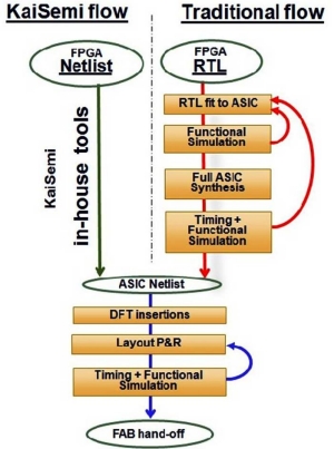
(September 17, 2010) — A breakthrough in automated FPGA-to-ASIC conversion allows fabless semiconductor company KaiSemi to provide customers with a seamless full turnkey ASIC solution, selling fully compatible replacement chips. KaiSemi’s process uses an in-house tool, which performs an automated conversion directly from the original FPGA netlist into a functionally identical ASIC gate-level netlist.

Click to EnlargeBacked by a tier-one fab vendor, KaiSemi’s automated conversion utilizes a database of multiple standard-cell fab process libraries. The wide range of libraries enables the conversion of any type and size of FPGA from any FPGA vendor to ASIC. This approach is accompanied by deep cost optimization during the automated conversion and allows the use of 3rd party standard hard cores (such as DDR interface, PCIe Phy, etc). The resulting ASICs — which are pin-compatible, timing-compatible, and functionally identical to the original FPGAs — consume less power and cost up to 70% less than their FPGA counterparts. Also read: Avoiding FPGA packaging problems, by John Rankin, AMI Semiconductor
KaiSemi’s automated conversion and flow eliminates the need for customer involvement and resources, NRE costs, long lead times, and the risks that are part of traditional FPGA-to-ASIC conversion flows. KaiSemi manages the whole FPGA-to-ASIC process for the customer, from the purchase order through conversion, the ASIC flow, manufacturing, all the way through to the shipment of the ASIC chips. This seamless conversion process – combined with the Zero NRE model – lets the customer order an ASIC chip as if it were an off-the-shelf second-source replacement chip with a relatively short lead-time.

"KaiSemi is focused on automating the process of converting any FPGA into an ASIC replacement chip while achieving the best cost solution in terms of price, power, area optimization, and the most appropriate fab process," said Gal Gilat, KaiSemi CEO.

KaiSemi’s team members originate in Flextronics-Semi’s conversion division, where they specialized in VLSI, EDA and FPGA-to-ASIC gate array conversions. The company’s conversions portfolio includes FPGA-to-ASIC, Multichip-to-ASIC, ASIC-to-ASIC, and DSP algorithm-to-ASIC.The company can convert multiple FPGAs into a single ASIC die. KaiSemi can also add peripheral die (such as memory) stacked with the FPGA replacement die in a single package. KaiSemi also handles ASIC-to-ASIC conversions, mainly for End-of-Life purposes. Additional offerings include migrating DSP algorithms to ASIC implementations via FPGA evaluations and prototypes.

KaiSemi is a fabless semiconductor vendor that specializes in selling replacement chips based on automated conversions. KaiSemi is a daughter company of the Kai-Tek Group.

Subscribe to Solid State Technology/Advanced Packaging.

Follow Advanced Packaging on Twitter.com by clicking www.twitter.com/advpackaging. Or join our Facebook group

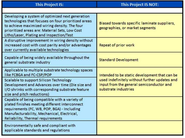
(September 16, 2010) — A pre-competitive iNEMI R&D project plan, currently under development, will identify approaches capable of meeting wiring density needs for future generations of organic semiconductor packaging substrates. Meeting these future needs will require radical improvements and innovations in all aspects of organic packaging substrate technology. A piecemeal approach will not be sufficient.

The iNEMI team has developed a preliminary Statement of Work and would like to present the current project plan to gather input and comments from a larger industry group and to assess the level of interest in participating in the project. The iNEMI organization held a preliminary workshop on organic substrates in 2009.

Click to Enlarge

A Webinar has been scheduled for Wednesday, September 22, 2010, starting at 5:00 PM Pacific Time (Thursday, September 23, 2010 at 8:00 AM in Asia). This meeting is open to anyone interested in reviewing and contributing to the plans. Copies of the draft Statement of Work will be distributed to everyone attending the webinar.

Use the following information to access the Webinar:

Topic: Wiring Density Program
Date:  Wednesday, 22 September 2010
Time: 5:00 pm, PDT (San Francisco, GMT-07:00))
Meeting Number: 739 591 924
Meeting Password: (This meeting does not require a password.)

To join the online meeting
1. Go to https://inemi.webex.com/inemi/j.php?ED=131958442&UID=0&RT=MiM0
2. Enter your name and email address.
3. Enter the meeting password: (This meeting does not require a password.)
4. Click "Join Now".

For assistance, contact Jim Arnold at:
[email protected]
Mobile: +1-480-703-0133
Tel: +1-480-854-0906

Please send a note to Jim Arnold if the time slot for the review is inconvenient. If there are enough people interested, additional review sessions will be scheduled. 

Follow Advanced Packaging on Twitter.com by clicking www.twitter.com/advpackaging. Or join our Facebook group

(Marketwire – September 15, 2010) — STATS ChipPAC Ltd. (SGX-ST: STATSChP) celebrated the grand opening of its new 300mm embedded Wafer-Level Ball Grid Array (eWLB) manufacturing facility. The official inauguration was held at STATS ChipPAC’s Yishun facility in Singapore with more than 150 local dignitaries, customer representatives, business partners and management participating.

In April 2010, STATS ChipPAC implemented 300mm eWLB wafer manufacturing capabilities. STATS ChipPAC’s robust, automated eWLB manufacturing process includes wafer reconstitution, wafer level molding, redistribution using thin film technology, solder ball mount, package singulation and testing. STATSChP has over 35 million eWLB units shipped to date.

The transition from 200mm to 300mm eWLB wafer manufacturing provides STATS ChipPAC cost and productivity benefits such as higher efficiency and economies of scale as compared to the existing 200mm eWLB reconstituted wafer format. STATS ChipPAC’s initial investment in eWLB technology totals more than US$100 million. The transition to 300mm eWLB manufacturing coincides with the company’s focus on increasing productivity per worker by more than two fold.

Earlier this week, Freescale announced a 300mm technology partnership for its wafer-level packaging (WLP) technology, RCP.

"We believe eWLB technology is quickly becoming the new advanced packaging solution that more customers are choosing to satisfy the relentless consumer market demand for complex and power efficient semiconductor devices in mobile phones and other handheld electronic products. Our goal is to deliver innovative, cost effective manufacturing technology to customers and help them rapidly ramp to volume production," said Tan Lay Koon, president and CEO, STATS ChipPAC.

STATS ChipPAC expects to continue to invest to further expand its eWLB capacity and capabilities over the next three years as the market demand continues to grow for small form factor, small footprint solutions with an increasing number of interconnects. Advanced fab technology nodes drive smaller silicon die sizes with finer interconnect pitches. The eWLB design advantage is that the package size is larger than the silicon die in order to provide sufficient area for the interconnection of the package to the application board. As a result, eWLB has the potential to realize a higher number of interconnects with standard pitches at multiple wafer technology nodes, according to the company’s statement.

STATS ChipPAC Ltd. is a leading service provider of semiconductor packaging design, assembly, test and distribution solutions in diverse end market applications including communications, digital consumer and computing. Further information is available at www.statschippac.com.

Follow Advanced Packaging on Twitter.com by clicking www.twitter.com/advpackaging. Or join our Facebook group

(September 13, 2010) — Package-on-package (POP) devices present some unique challenges with respect to the rework process: one of these is how to rework an underfilled package; also, these packages are prone to warpage. Lastly, the challenge of inspecting the area array devices can be overcome with highly trained personnel with experience in the BGA rework area. Bob Wettermann, BEST Inc., discusses rework solutions.

Stacking semiconductor packages suits various applications requiring smaller footprints, greater functional density, and higher performance. Consumer products using flexible package design include digital cameras, portable game players, GPS products, and smartphones. When these devices need to be repaired or upgraded or reworked, PoP packages require a robust, cost-effective, reliable rework process. This article discusses rework solutions.

PoP packages present some unique challenges with respect to the rework process: one of these is how to rework an underfilled package; also, these packages are prone to warpage. Lastly, the challenge of inspecting the area array devices can be overcome with highly trained personnel with experience in the BGA rework area.

Underfill

The rework of underfilled POPs is a major challenge as most of the underfill materials are epoxy-based. These epoxies need to be heated above their softening temperature (above 150°C) and along with this heat a mechanical force needs to remove this previously cured material. The material removal can be accomplished through high temperature vacuum extraction or hand tools, depending on the modulus of elasticity and underfill’s softening temperature.

The most commonly used underfill rework process begins with even substrate heating to a temperature above the underfill’s softening point. The package is mechanically gripped or pried with enough torque to break the fillet’s adhesions to the PCB. The chip undergoing rework is then heated above the solder reflow temperature to melt the solder connections and break the softened underfill. The device is removed from the PCB and residual solder and underfill cleaned off the substrate. Cleanup after chip removal removes any underfill, as well as excess solder on the substrate. This part of the process must be done with extreme care so as not damage the pads and adjacent components on the substrate. The site is then cleaned prior to inspection. Once substrate cleanup is complete, a new chip can be aligned, reflowed, and underfilled. The manual nature of this process — both heat and mechanical forces being used — results in less than a 50% yield in the best of cases.

Click to Enlarge
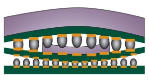
Figure 1. Warped package-on-package (POP).

Warpage

POP packages, due to their thin construction, are subject to warpage during initial assembly as well as rework. During the package-to-board placement process, if the lower package substrate flexes downward at its edges the solder ball contacts mating with the PCB can collapse to the point of collapsing together and creating a shorting condition (Fig. 1). Similarly, if the second-level package substrate warps in the opposite direction of the lower package, the solder will elongate and possibly separate.

Inspection and X-ray

Most contract rework houses or assembly houses have 2D X-ray as part of their normal non-destructive process control measures. By reviewing the ball diameters for consistency, problems in the rework process can be discovered. The trick is to make sure that the actual images being reviewed are all at the same layer. This can be difficult with a transmissive X-ray as the exact location of where the ball images show up in the Z-axis is difficult to confirm. All of the device layers are seen at the same time in the same X-ray image, so lower layers can be obscured by upper layers.

In some X-ray systems, oblique angle views (tilting the part or tilting the X-ray source) may be useful, but only to a limited extent. Layers placed further away from the X-ray tube will be seen as smaller than the closer layer; this phenomenon (known as geometric magnification) coupled with the different ball diameters of the different layers makes for very confusing X-ray images. Even when using a laminographic method (i.e., “slicing” of different x-ray image layers), there is not the resolution required to determine which ball sizes are to specification and which are not.

The challenges of inspection, part warpage and underfill removal without part all complicate the rework of POP devices. There are a few different methods being used to the rework process.

Click to Enlarge
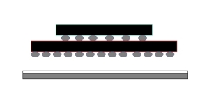
Figure 2. Stacking one layer at a time method of POP rework.

Different rework methods

There are two basics processes being used in the rework of POPs, namely: a “stack” of the multiple layers is pre-made and the device is then placed like a standard area array device (Fig. 2 “Stack one layer at a time”); or the first layer of the stack is placed onto the board and then the subsequent layer(s) of the stack are placed on top of the first. In either case, accurate and repeatable placement accuracy, the right materials, and tight process controls, are required to generate first pass yields over 95%.

Stack rework method. In the stack method, the devices are first assembled together and then placed as a single entity on the board location to be reworked. Starting with the package that is closest to the base package (the one that will be soldered to the PCB), solder paste is dipped into a reservoir to a depth of 40-50% of the ball diameter. The solder paste volume is controlled by ensuring that the reservoir is filled prior to each “dip” and that the depth to which the package is submerged is tightly controlled. Many rework stations can control this depth by having it “bottom out” in the reservoir. The nozzle then places the package on top of the base device. Finally, the stack is reflowed, cleaned and inspected. These steps are repeated for any subsequent packages that need to be placed onto the stack. Once the stack has been completed, the last step is attaching this “stack” to the PCB. Paste printing with either a removable stencil, or, for greater paste volume and prevention of shorts, a stay-in-place polymide stencil may be used to attach the stack to the PCB.

Layer rework technique. In this rework technique, each layer of the stack is individually placed one after the other beginning with the device being attached to the PCB, stacking the layers until all of the PoP elements have been placed. For the base layer, the PCB is paste-printed using either a peel-and-release type of stencil, or a stay-in-place polyimide stencil. Subsequent packages can have either paste flux or dipping solder paste applied, be aligned to the next layer in the stack, and then placed. Once all of the layers have been placed, the entire stack is reflowed. The benefit of this approach is that the die are only exposed to a single reflow and intermetallic growth in other layers is limited, increasing the probability of good device reliability.

Rework materials

There are several types of soldering materials that are recommended for use in the rework of POPs: solder paste, newly developed “dipping” pastes or fluxes, or paste flux.

Solder dipping paste used in the dipping process has different rheological properties than paste used for standard surface mount assembly. The dipping paste is lower in viscosity than that designed for printing or dispensing. Pastes with 75-80% metal content and type IV particles (20-38µms in diameter) work best for dipping.

Fluxes used in POP rework also have modified properties when compared to the standard BGA rework paste fluxes. The typical POP flux is a water-soluble, no-clean formulation containing a mild- to medium-active organic acid. When formulating tacky flux, suppliers must balance viscosity and elasticity so the material can be spread in a flat, even film for dipping. If the material is too thick, the film will have streaks or voids. If it’s too thin, the film won’t hold its shape or maintain an even thickness over time.

Click to Enlarge
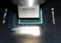
Figure 3. Dipping paste used to attach one layer on to next.

Dipping process for POPs

When “dipping” style fluxes and pastes are used in the rework of PoPs the rule of thumb is to dip transfer 40% of the ball diameter (Fig. 3). Compared to the printing process, dip transfer techniques transfer less solder paste volume. The dip method has a smaller process window compared to the printing process, and is therefore more susceptible to yield detractors, including poor dipping volume control for heavier parts and incorrect paste flux tack properties. The data implies that you are only likely to see an issue with the pick up PoP components from a dipping PoP flux tray if components are too heavy, if the vacuum nozzle is too small, or the flux has high tack properties.

In cases where underfills need to be applied underneath the device package, flux will not work. Since the lack of cleaning under the package prevents the underfill material from spreading completely there, flux is not recommended.

PoP rework recommendations

To overcome the numerous POP rework challenges, proper process techniques using good process control methods must accompany these materials.

There are several precautions you can take during POP rework to overcome warpage effects. One of the recommendations is to use a solder paste when placing the entire “stack” onto the board, or even in between the various layers. On the board location, this paste printing is recommended for maximum solder volume application. In between stacks, a “dippable” Fig. 3 solder paste can be used to increase the solder volume in the solder joint and therefore insure a greater process window. Finally, one can use a polyimide stay-in-place stencil that allows both a greater, more consistent volume of solder paste to be printed, and prevents the shorting of balls as a dielectric barrier is formed around each of the balls. These rework methods can be used to help overcome the negative impacts of POP package warpage during the rework process.

When attempting to rework a POP that has been underfilled, this very labor-intensive, low-yielding process many times makes the rework process undesireable. The epoxy and other material underfills require the use of both heat and mechanical force to remove. This combination ultimately either damages the part or the board, creating either more repair, or causing the board to be scrapped. Therefore, extreme dexterity of the rework operator is required to overcome this challenge.

There are challenges in inspecting a POP device after the rework process has been completed. For instance, some balls are “hidden” behind others in the x-ray image, or the inspector may be confused on which ball is on which layer. This problem can be somewhat mitigated by oblique angle views on the x-ray system. While not seeing all of the layers completely clearly, oblique angle viewing will have the propensity to show defects such as head in pillow (HIP) failures, and clearer indication of any opens.

Click to Enlarge
Figure 4. POP post-rework.

Conclusion

There are numerous rework challenges associated with POP devices. The problems of part warpage, proper inspection post-rework, as well as the rework of underfilled devices, are certainly challenging. They can be overcome to a great degree by using the proper materials; methods; and highly trained, skilled rework technicians.

References
[1] R. Boulanger, “Assembly Challenges of Package-on-Package,” Proc. of SMTA International Conf., 2006, pp.338-341.
[2] P. Wood, “Reworking Package on Package Components,” Proc. of SMTA International Conf. 2007, pp.363-367.
[3] L. Smith, M. Dreiza, A. Yoshida, “Package on Package (PoP) Stacking and Board Level Reliability Results,” Proc. of SMTA International Conf. 2006, pp.306-312.
[4] H McCormick, I. Sterian, J. Chow, M. Berry, J. Trudell, R. Cortero, “PoP: An EMS Persepctive on Assembly, Rework and Reliability,” Proc. of SMTA International Conf. 2008, pp.102-113.

Bob Wettermann received his BSEE University of Illinois, MBA DePaul University and is QC Manager at BEST, 3603 Edison Place, Rolling Meadows IL 60008; ph.: 1-847-797-9250; [email protected]

Follow Advanced Packaging on Twitter.com by clicking www.twitter.com/advpackaging. Or join our Facebook group

(September 13, 2010 – BUSINESS WIRE) — Freescale Semiconductor will license its redistributed chip packaging (RCP) technology to Nepes Corporation, a Korean semiconductor parts and materials specialist. Nepes and Freescale will also collaborate on RCP development.

Nepes installed the 300mm equipment set and manufacturing process capable of multiple-layer single-die and multi-die system-in-package (SiP) solutions at its facility in Singapore (Nepes Pte) earlier this year. The technology start-up at Nepes is in progress with a volume ramp forecast for the first quarter of 2011. Using RCP on 300mm wafers is expected to lower costs for the advanced packaging technology.

Freescale and Nepes are also collaborating in a joint development effort to further enhance the capabilities of the RCP technology. Development activities are expected to continue at both Freescale’s US RCP development facility in Tempe, AZ and at Nepes’ facility in Singapore. Advanced Packaging blogger Dr. Phil Garrou notes that, "During the recent hard economic times, Freescale scaled back their process work and eventually licensed their process to Nepes." (Read Insights from the Leading Edge, Dr. Garrou’s blog, here)

The collaboration will enable single die, 2D, and 3D systems-in-package targeted at a broad range of industries and applications.

Freescale, which developed and introduced the now widely deployed ball grid array (BGA) packaging technology, announced the RCP technology in 2006. Fan-out RCP integrates semiconductor packaging as a functional part of the die and system solution. RCP is a substrate-less embedded chip package that offers a low-cost, high performance, integrated alternative to current wire bond BGA and flip chip BGA packaging. Semiconductor devices are encapsulated into panels while routing of signals, power and ground is built directly on the panel. The RCP panel and signal buildup lower the cost of the package by eliminating wafer bumping and substrates, thereby enabling large scale assembly in panel form. The buildup provides better routing and integration capabilities than traditional printed circuit boards (PCB) or high density interconnect PCBs. By eliminating chip to package bumping, the package is inherently lead-free and the stress of the package is reduced enabling ultra-low-k device compatibility.

It addresses some of the significant limitations associated with previous generations of packaging technologies by eliminating higher cost wire bonds, package substrates and flip chip bumps. In addition, RCP does not utilize blind vias or require thinned die to achieve thin profiles. These advancements simplify assembly, lower costs and provide compatibility with advanced wafer manufacturing processes utilizing low-k interlayer dielectrics.

The RCP fan-out package provides solutions for both highly sensitive analog devices and digital platforms. The technology is compatible with small and larger package sizes. RCP accommodates single and multiple routing layers to optimize package size, performance, die size range of I/O and cost.

Research and Markets recently published a report on embedded and fan-out wafer-level packaging (WLP)

Key advantages of RCP include:

  • Improved electrical performance resulting from shortened routing distances and reduced contact resistance.
  • Reduced cost due to elimination of wirebonds, large batch processing and simplified assembly process.
  • Reduced assembly stress suitable for packaging low-k dielectrics increasingly common on modern semiconductor die.
  • RCP results in a “green” product, halogen and lead-free and RoHS compliant.
  • Enables the reduction of die size due to an improvement in package performance.
  • RCP technology can be highly integrated allowing for single-die, multi-die SiP, stacked packages and other 3D integrated packaging solutions.

Nepes is a major back-end supplier in the system LSI semiconductor market, providing technology ranging from display driver ICs to wafer level packages on 8" and 12" wafers. Nepes, based in South Korea and Singapore, performs 300mm flip-chip bumping (lead-free and eutectic solder), wafer level BGA (WLBGA), Au redistributed layer, 40um pitch micro bumping, and copper pillar. For more information, visit www.nepes.co.kr and www.nepes.com.sg.

Freescale Semiconductor designs and manufactures embedded semiconductors for the automotive, consumer, industrial and networking markets. Learn more at www.freescale.com

Also read:

Convergence of 3D integrated packaging and 3D TSV ICs by Navjot Chhabra, Freescale Semiconductor

Follow Advanced Packaging on Twitter.com by clicking www.twitter.com/advpackaging. Or join our Facebook group

(September 10, 2010) — Speaking at the MEPTEC Forecast Luncheon (Santa Clara, CA 9/8/10), Gartner VP of semiconductor manufacturing research, Jim Walker, noted that equipment spending is mostly on technology, foundry and memory. And for the first time, 2 SATS companies (ASE and SPIL) joined the top 20 capital spenders in 2010. He also predicts solid growth for advanced packaging tooling with memory ATE and copper wire bonders being the top performers. Walker told attendees that the conversion to copper wire from gold is a wise move for the industry — with even some high-end packaging joining the conversion.

Podcast: Download or Play Now

Overall, Gartner sees a 31.5% semiconductor growth in 2010, with PCs, cell phones, and LEDs being the key drivers. (Also listen to an interview with Bob Johnson, Gartner, here)

Hear additional comments on the forecast and the overall economic outlook in the podcast interview with Walker, including his thoughts on how the memory cycle will impact capex.