Category Archives: Wafer Level Packaging

May 10, 2011 – Marketwire — RFaxis, a fabless semiconductor company focused on RF for wireless connectivity and cellular/mobility markets, released its patent-pending On-Die Coexistence Filter technology. When combined with RFaxis’ on-die transmit circuitry, the on-die coexistence filter helps reduce circuit board area, lower current consumption, and simplify bill of materials (BOM).

The packaging technology targets multifunction WLAN/Bluetooth/WCDMA cellular devices such as smartphones, tablets and other mobile internet devices.

"Conventional coexistence filters are bulky and expensive standalone components, and have always been a challenge for multifunction cellular device OEMs and ODMs in terms of lowering BOM costs, optimizing wireless performance and accelerating design cycles," stated Mike Neshat, chairman and CEO of RFaxis, who adds that On-Die Coexistence Filters eliminate an external companion component for the cellular RF front-end.

Dr. Oleksandr Gorbachov, RFaxis CTO, adds, "By integrating our new Coexistence Filter technology into our CMOS RFeIC single-die circuits for multifunctional cellular devices, RFaxis is able to reduce transmit power loss by at least 1.5dB at the antenna, significantly improve receive sensitivity, and substantially reduce current consumption by tens of milliamps. This translates into extended battery life and robust performance while saving PCB real estate."

RFaxis Inc. specializes in the design and development of RF semiconductor and embedded antenna solutions. More information can be found at www.rfaxis.com.

Subscribe to Solid State Technology/Advanced Packaging.

Follow Advanced Packaging on Twitter.com by clicking www.twitter.com/advpackaging. Or join our Facebook group

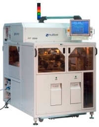
May 6, 2011 — Multitest, a designer and manufacturer of final test handlers, contactors and load boards used by integrated device manufacturers (IDMs) and final test subcontractors, provides extended temperature control with its extended temperature calibration (XTX) on the MT9510 test handler.

Click to EnlargeActive thermal control systems are often not appropriate for medium range power dissipation control for devices under test (DUT). Some semiconductor manufacturers develop proprietary solutions, but Multitest is offering a turnkey solution.

Multitest’s extended temperature calibration (XTC) offers for medium range power dissipation of up to 50W. The die temperature inside the DUT is stabilized at a set temperature and a temperature drift after contacting is avoided.

The XTC is integrated into the conversion kit. Besides cost efficiency, this also ensures the full availability for any MT9510 pick-and-place handler in the market.

For more information about Multitest’s XTC capability on its MT9510, visit www.multitest.com/MT9510.

Also read: Multitest ECON contactor exceeds 4.5M insertions

Subscribe to Solid State Technology/Advanced Packaging.

Follow Advanced Packaging on Twitter.com by clicking www.twitter.com/advpackaging. Or join our Facebook group

May 6, 2011 – Marketwire — Cascade Microtech, Inc. (NASDAQ: CSCD), wafer-level test & measurement provider, launched the Viper probe card series. Viper probe cards will be used for test of high-volume production wafer-level chip-scale packages (WLCSP). Viper’s probe pin is integrated into Cascade Microtech’s proprietary laminated housing for consistently good electrical results.

Users can easily scale from x1 to x8 and beyond on a per-die basis as production ramps, without changes to the layout of the multi-site probe card. Unlike traditional spring pin solutions, the Viper architecture features patented housing that ensures the pin is retained, maintaining tip position accuracy for consistent contact resistance and low inductance. The patented non-rotating pin reduces PCB pad wear, delivering a longer probe card lifetime.

Individual contact engines are replaceable on a per-DUT basis, requiring no special tools or microscopes. The Viper probe head can also be configured with the ‘Accel’ option, which allows for individual die testing, shortening test program development and enabling re-test of individual die. Also read: Accel-RF debuts reconfigurable RF test fixture

In smart phones, combo chips provide Bluetooth, WLAN, near-field communication and digital TV functionality. Combo chips predominantly use chip-scale and WLCSP packaging techniques, which demand high-performance known good die (KGD) testing.

WLCSP is the fastest-growing package style, and demand is outpacing the available market capacity. According to Yole Developpement, WLCSP accounts for more than 6% of all IC packages worldwide, and growth is expected to reach 15-20% within the next decade. The WLCSP market is dominated by optical, analog, and RF wafer-level package applications. IC manufacturers need cost-effective production strategies that ensure the highest quality, and to keep pace with demand to reduce the total test cost of ownership.

Cascade Microtech, Inc. (NASDAQ: CSCD) makes tools for precise electrical and mechanical measurement and test of integrated circuits (ICs) and other small structures. Cascade Microtech’s semiconductor production test products include unique probe cards and test sockets that reduce manufacturing costs of high-speed and high-density semiconductor chips. For more information visit www.cascademicrotech.com.

Subscribe to Solid State Technology/Advanced Packaging.

Follow Advanced Packaging on Twitter.com by clicking www.twitter.com/advpackaging. Or join our Facebook group

May 5, 2011 — Semiconductor Research Corporation (SRC), university-research consortium for semiconductors and related technologies, is leading an effort to address key roadblocks for wide-scale adoption of the emerging 3D integration of integrated circuits (IC) and systems. These new initiatives will address critical reliability and design tool issues and leverage a partnership formed by researchers from universities and the semiconductor industry at large.

3D technologies can offer disruptive benefits and breakthroughs on the same level as the integrated circuit itself, said Jon Candelaria, director of Interconnect and Packaging Sciences at SRC.

Reliability issues for these emerging 3D integration platforms are not merely extensions of conventional 2D IC technology issues, but also bring many unique and complex challenges that require innovative solutions.

In addition, the sophisticated software tools created and developed over the years to design more complex 2D integrated circuits systems will not extend easily to 3D. The challenges include the optimization of each layer of circuitry that could be stacked together, the partitioning and placement of each of billions of individual devices and the routing and timing of signals to all of these.

"SRC’s support and management of an extensive research portfolio in these and many other related areas uniquely qualify us to lead these new initiatives working with our university and industry colleagues, and we expect this effort to play a key role in the short term while having an even greater long-term impact," Candelaria said.

SRC is driving these initiatives as a part of the 3D Enablement Center program in partnership with SEMATECH and the Semiconductor Industry Association (SIA). The program aims to establish the infrastructure, including industry standards and specifications, necessary for the industry to leverage 3D packaging technology for innovative new applications, as well as for enabling smaller, faster and lower-power ICs for existing product families.

SRC defines industry needs, invests in and manages the research that gives its members a competitive advantage in the dynamic global marketplace. Awarded the National Medal of Technology, America’s highest recognition for contributions to technology, SRC expands the industry knowledge base and attracts premier students to help innovate and transfer semiconductor technology to the commercial industry. For more information, visit www.src.org.

Also see: If wide I/O DRAM and other 3D technologies can go HVM, standards are needed

Subscribe to Solid State Technology/Advanced Packaging.

Follow Advanced Packaging on Twitter.com by clicking www.twitter.com/advpackaging. Or join our Facebook group

May 5, 2011 – Marketwire — Tektronix Service Solutions, single-source provider of instrument calibration, repair and related services, was chosen by NXP (NQ:NXPI) to provide calibration and repair services for all test and measurement instruments at NXP’s production and development sites in the Netherlands.

The contract will be managed by the Fluke Service operation in Eindhoven on behalf of the Service Solutions Organization and will allow NXP to focus on its core business, leaving the calibration of its test and measurement instruments to the experts.

"Metrology plays a crucial role in the development and production of our products, and it is therefore vitally important to ensure that our test instruments are well-maintained and calibrated," said Leon Sintnicolaas, GM of the European Quality Labs at NXP Semiconductors. "When we decided to outsource the maintenance and calibration of our equipment…we chose Tektronix Service Solutions to take over this contract because we felt that they were able to offer the expertise and reliability we were looking for."

Tektronix Service Solutions provides asset management, calibration, repair, product and compliance testing, and quality certification. The company combines the service capabilities of Tektronix, Fluke and multi-vendor service teams of Davis Calibration and Sypris Test & Measurement into a single, service-focused organization. Learn more at http://service-solutions.tektronix.com/.

Subscribe to Solid State Technology/Advanced Packaging.

Follow Advanced Packaging on Twitter.com by clicking www.twitter.com/advpackaging. Or join our Facebook group

May 4, 2011 — CAD Design Software Inc., mechanical and electrical design tool maker, combined its Electronics Packaging Designer (EPD) and Cadence Design Systems’ Allegro IC Package design and analysis environment to create a "Silicon Realization" flow for ICs in leadframe packages.

Newer low-cost leadframes can be used to package ICs with higher IO counts. Lead frame designs with IO counts in the hundreds require Silicon Realization tools that enable chip/package/board co-design, complex wirebonding with 3D design rule checks, and characterization and modeling tools. CAD Design Software integrates mechanical design packages, where a typical leadframe package is initially designed, with the Cadence Allegro IC Packaging tools where constraint-driven organic and ceramic substrate packages have typically been designed.

Freescale Semiconductor is an early adopter of the converged solution and helped refine the flow. "The collaboration between CAD Design Software and Cadence has greatly reduced the difficulty in designing complex Lead Frame packages. This integration has significantly reduced our design cycle time," reported Neil Tracht, Freescale design manager.

CAD Design Software’s Electronics Packaging Designer (EPD) AutoCAD-based software suites are tailored to applications such as PCB, Flex, Lead Frame, Ceramic (Hybrid/MCM/ LTCC/Thick Film/Thin Film), RF/Microwave, IC Packaging, IC Test, CAM and other design technologies. CAD Design Software is a subsidiary of CAD Design Services Inc. More information about the company, its products, and services is available at www.CAD-Design.com.

Subscribe to Solid State Technology/Advanced Packaging.

Follow Advanced Packaging on Twitter.com by clicking www.twitter.com/advpackaging. Or join our Facebook group

May 4, 2011 – MarketwireSTATS ChipPAC Ltd. (SGX-ST: STATSChP), semiconductor test and advanced packaging service provider, has shipped over 300 million semiconductor packages with copper wire-bond interconnects. The SATS provider is investing in Cu wire bonding for finer silicon nodes (45/40nm) and low-k/extra low-k (ELK).

STATS ChipPAC is investing in equipment and resources to support copper wire technology in wafer nodes down to 45/40nm with low-k and ELK dielectric materials. Development work is focused on finer bond pad pitches, thinner wire diameters, stacked die packaging and die-to-die bonding, each of which represents a greater set of challenges in the application of copper wire.

The transition from gold to copper wire interconnect in semiconductor packages offers a significant savings in material costs while meeting electrical and thermal performance characteristics with quality and reliability standards that are comparable to gold wire, the company states. STATS ChipPAC has copper wirebond capabilities in all five of its manufacturing facilities in Asia, each with class 1000 cleanroom environments.

Production volume has been rapidly increasing in both leadframe and laminate packages. "We are in high-volume manufacturing for a large number of devices across multiple factories and have built significant momentum on the engineering front to introduce copper wire into a wider range of applications in the communication, computing and consumer markets," said Hal Lasky, EVP and chief sales officer, STATS ChipPAC.

"We are successfully addressing many of the technical challenges that are associated with using copper wire interconnect in more complex package structures. We have been aggressively developing copper wire capabilities in all our factories and rapidly expanding into a broader range of fine pitch devices and advanced silicon nodes. Our dedicated resources, especially our strong global copper wire engineering organization, ensure a consistent and successful transition to copper wirebond for our customers," said Dr. Han Byung Joon, EVP and chief technology officer, STATS ChipPAC.

STATS ChipPAC Ltd. is a leading service provider of semiconductor packaging design, assembly, test and distribution solutions in diverse end market applications including communications, digital consumer and computing. With global headquarters in Singapore, STATS ChipPAC has design, research and development, manufacturing or customer support offices in 10 different countries. STATS ChipPAC is listed on the SGX-ST. Further information is available at www.statschippac.com

Also read: Cu wire bonding joins MagnaChip Semiconductor offerings

K&S: Enabling high-volume fine-pitch Cu wire bonding

Subscribe to Solid State Technology/Advanced Packaging.

Follow Advanced Packaging on Twitter.com by clicking www.twitter.com/advpackaging. Or join our Facebook group

May 3, 2011 – Marketwire — GN ReSound, a technology leader in hearing aid solutions, has contracted with eSilicon Corporation, independent semiconductor Value Chain Producer (VCP), for the production of the AD4.0 ASIC. This ASIC is a key component in next-generation hearing instruments from GN ReSound.

Exceeding sales projections for the Alera hearing instruments prompted GN ReSound to seek an experienced ASIC partner that could manage the ASIC manufacturing and back-end production, optimize current costs, uphold high quality standards, and deliver product on time, said Peter Vuust, director of corporate purchase at GN ReSound. "The big bonus was access to work in progress through the eSilicon Access production management system that allows 24/7 visibility into the status of the products as they move through the production phase."

A Value Chain Producer (VCP) is a company that collaborates with foundries, IP and service providers, EDA suppliers, package, assembly and test operations in designing and producing chips for fabless IC, IDM and OEM companies.

eSilicon,independent semiconductor Value Chain Producer (VCP), delivers ASICs to OEM and fabless semiconductor companies through a flexible, lower-risk path to volume production by deploying its comprehensive suite of design through manufacturing services. For more information, visit www.esilicon.com.

GN ReSound is a industry technology leader in hearing solutions. Learn more at http://www.gnresound.com

Subscribe to Solid State Technology/Advanced Packaging.

Follow Advanced Packaging on Twitter.com by clicking www.twitter.com/advpackaging. Or join our Facebook group

May 2, 2011 – BUSINESS WIRE — Flexpoint Sensor Systems Inc. (OTCBB: FLXT) received a development order from the National Aeronautics and Space Administration (NASA) to supply their patented Bend Sensors.

Flexpoint was unable to reveal the application in which NASA is using Bend Sensors, though Clark Mower, president of Flexpoint, called the project a "new and expansive area of potential use of our technology."

This product will be delivered to NASA during the current quarter.

Traditional sensor (left) and Bend Sensor (right).

The single-layer flexible Bend Sensor product allows for measurement of mechanical movement, air flow, water flow, or even vibration. In addition, it has been tested to over 35 million cycles without failure. It can be used as a range of motion sensor, or as a switch in most harsh environments.

The Bend Sensor comprises a coated substrate, such as plastic, that changes in electrical conductivity as it is bent. Electronic systems connect to the sensor and measure bending or movement. The single-layer design eliminates problems associated with conventional sensors such as dust, dirt, liquids, and heat and pressure effects. Over-laminates or over-molding may also be applied to the sensors for added environmental protection.

Flexpoint Sensor Systems (FLXT) is a leading supplier of thin film sensing technology to many industries, including automotive, medical, industrial controls, and consumer products. Learn more at http://www.flexpoint.com

Subscribe to Solid State Technology/Advanced Packaging.

Follow Advanced Packaging on Twitter.com by clicking www.twitter.com/advpackaging. Or join our Facebook group

Executive Overview

Redistribution technology was developed out of necessity to allow fan-in area array packaging (bumping) to take hold when very few chips were being designed for area array. In the intervening years it has been instrumental in developing many of the newer packaging technologies such as wafer-level packaging (WLP), fan-out packaging, and TSV-based interposers and chip stacks.

Philip Garrou, Microelectronic Consultants of North Carolina, Research Triangle Park, NC USA; Alan Huffman, RTI Int., Research Triangle Park, NC USA

The concept of flip-chip (FC) can be traced back to what IBM called "controlled collapse chip connection" (C-4) in the late 1960s. It has always been clear that FC is a superior interconnect based on size, I/O density, electrical and thermal performance. However, during the 1960s-1980s, the technology was mainly confined to high end main frame computer companies because the CTE mismatch between Si and PWB laminate required that FC use expensive ceramic packaging.

For FC to find widespread acceptance by those interested in miniaturized portable products such as lap tops, cell phones, pagers, camcorders etc., reliable lower cost FC processes were needed. In the early 1990s, IBM Japan reported that FC chips could be reliably attached directly to PWB laminate if the chips were underfilled. Unitive and Flip Chip Technologies (FTC) subsequently developed lower cost UBMs, lower cost solder deposition technologies (FCT – stencil printing; Unitive – plating) and redistribution (RDL). The FCT and Unitive technologies were licensed by all the key assembly houses including ASE, Amkor, STATSChipPAC and SPIL, as they initiated production in the early 2000s. This brought flip-chip technology to the masses.

RDL

The lack of area array designed chips was a major impediment to the early use of FC. RDL addressed this issue (Fig. 1) − defined by the addition of metal and dielectric layers onto the surface of the wafer to re-route the I/O layout into a new, looser pitch footprint. Such redistribution requires thin film polymers (BCB, PI or newer polymers such as Asahi Glass ALX) and metallization (Al or Cu) to reroute the peripheral pads to an area array configuration.
Click to Enlarge

Figure 1. Bumping RDL.

The redistribution trace can be fabricated directly on the primary passivation (SiN or SiON) or can be routed over a second layer of polymer to add additional compliancy.

It was widely assumed at the time that RDL was a stopgap measure and its use would quickly diminish as chip designs migrated to area array. Indeed, RDL is used very little for bumped chips today (estimated at <5% of bumped chips by Amkor and FCI) but as we shall see, it has found a home in other advanced packaging technologies.

To incorporate high I/O FC devices onto a standard PWB, one was still required to use a package, such as a BGA, to serve as an interposer, matching the chip I/O pitch with the pitch on the PWB.

It was discovered, however, that in low I/O devices, RDL could relax the I/O pitch on the chip and allow direct attachment to the PWB. To mitigate CTE stresses and avoid the use of underfill (slows throughput), larger diameter solder balls (250µm+ diameter) were used for this packaging. This low cost solution proved to be reliable for up to 5mm chips. This concept was first proposed by Sandia Labs in 1994 and called the mini BGA. The first commercialization of such a product was the FCT Ultra CSP, which was introduced in 1998. Soon afterward, Unitive came out with its Xtreme CSP. Over time, the nomenclature for such structures changed from mini-BGA, to wafer-level chip scale package "WL-CSP," to the simpler, wafer-level package "WLP" [1,2].

Fan-out packaging

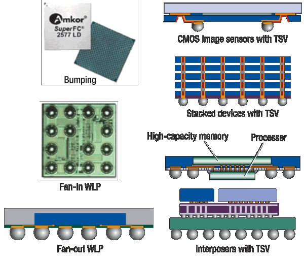
In the early 2000s the question became how to use the WLP concept when larger numbers of I/O were required or how to maintain the same I/O and pitch during a die shrink. So called "fan-out" packaging (vs. traditional WLP, which is now called fan-in since all the I/O have to fit within the dimensions of the die) was developed to deal with this issue.

Infineon’s embedded wafer-level BGA (eWLB) and Freescale’s redistribution chip package (RCP) are two examples of fan-out WLP that have received significant industry attention. Infineon has licensed eWLB to STMicro, STATSChipPAC, and ASE. Freescale has licensed the RCP process to Nepes.

Click to Enlarge

Figure 2. Examples of advanced packaging technologies using RDL.

In the eWLB process a carrier wafer is laminated to dicing tape and known good die (KGD) are placed face down to create a "reconfigured wafer." This wafer is then compression molded to encapsulate it and the wafer carrier and tape are removed. The molding compound is used to carry the fan-out area and to protect the chip backside. An RDL (Fig. 2) is created on the now exposed die faces, the I/O are rerouted, solder balls are placed, and the die are singulated.

3D stacking with TSV

For the last few decades, IC technology has used shrinking gate dimensions and decreasing operating voltage to improve gate switching delay and thus device performance. As we look beyond the 32nm node, we find that fewer and fewer foundries/IDMs can afford to put <45nm generations of technology into place. In addition, further scaling has resulted in increased line resistance and capacitance for the smaller cross-section wires. Options to improve performance, at a reasonable cost, have become limited.

One solution that has been proposed is 3D Integration, where multiple layers of planar devices are stacked and interconnected through the silicon [3]. The resulting decreased chip area results in much shorter global interconnect, which results in less power required to drive signals the shorter distance.

Once the infrastructure is in place, it is hoped that 3D IC technology will reduce both risk and cost through economic benefits such as: a) reducing the time it takes to design and verify chips at the most advanced nodes; b) allowing the use of older analog IP blocks rather than having to develop new IP blocks at the most advanced process nodes; and c) allowing the mixing of normally incompatible technologies (heterogeneous integration).

Three-dimensional technology can enable the integration of current off-chip memory (like L2 cache) onto the processor chip, thereby eliminating some of the slower and higher-power off-chip buses to off-chip memory and replacing them with high-bandwidth, low-latency vertical interconnections. In addition, on-chip memory (embedded) can be fabricated on a separate layer and bonded to the logic functions. Both of these options improve access latency, the former reducing interconnect length from tens of millimeters to tens of microns, and the latter allowing optimization of memory processing on a separate layer.

The key enablers of 3D include: 1) fabrication of the through silicon vias; 2) thinning the die/wafers to 50µm or less; 3) align and bond the die/wafers, usually through some form of metal-metal bonding. TSVs will be manufactured either in the fab/foundry during back end of line (vias middle), or after the die has been completed from the back side of the wafer (vias last-backside) by the foundry or OSAT (outsourced semiconductor and test). Backside TSV processing includes insulation and metallization of the TSV, backside RDL and bump placement. For the TSV last-backside processes, OSATs can use their standard polymer-based RDL processes, with minor alterations, to fabricate these structures. An example of this is STMicro’s 300mm CMOS image sensor line in Crolle.

While stacking of die, such as memory, is made easier by having identical I/O, stacking other chips will require an I/O interface standardization that is not yet in place. In order to mate such die, silicon interposers with RDL (single or double-sided) are used. It is expected that interposers will function as a stop gap until standardization is in place to allow full wafer/die stacking. Recent commercialization announcements of 3D stacked memory have come from Elpida and Samsung. Product announcements using interposers have come from Xilinx (TSMC manufacturing the interposer) and IBM fabricating interposer-based modules for Semtech.

Conclusion

While the initial use of RDL for fan-in die bumping has indeed diminished over the years since its inception, RDL technology has been instrumental in the development of many advanced packaging technologies such as fan-in and fan-out WLP, and TSV applications such as CMOS image sensor packaging, silicon interposers for 3D integration, and 3D integration with backside TSV.

Acknowledgments

Ultra CSP is a trademark of Flip Chip Technologies, and Xtreme CSP is a trademark of Unitive.

References

1. P. Garrou, "Wafer Level Packaging has Arrived," Semiconductor Int., Vol. 23, no. 12, 2000, p. 119.

2. P. Garrou, "Wafer Level Chip Scale Packaging (WL-CSP): An Overview," IEEE Trans. Advanced Packaging, Vol. 23, 2000, p. 198.

3. "Handbook of 3D Integration", P. Garrou, C. Bower, P. Ramm Eds., Wiley VCH, 2008.

Biographies

Philip Garrou received his BS in chemistry from NC State U. and his PhD in chemistry from Indana U. and is Sr consultant at Microelectronic Consultants of NC, RTP, NC 27513 USA; ph. : 919-248-9261; email [email protected].

Alan Huffman received his BS in physics from the U. of North Carolina and is with RTI International, RTP, NC USA. 


More Solid State Technology Current Issue Articles
More Solid State Technology Archives Issue Articles