Category Archives: Wafer Level Packaging

April 28, 2011 — New Venture Research will release "The Worldwide IC Packaging Market, 2011 Edition" in May 2011. It offers an in-depth look at the worldwide integrated circuit (IC) packaging market.

The forecasts of individual IC device markets are provided, for units, revenue, and ASP, from 2008 through 2014.

The packages for each of these markets are then forecast, broken down into I/O ranges.

In a separate chapter, the package types are rolled up to deliver an overall worldwide forecast of IC packages, divided into 12 different package families, plus bare die solutions. The major package families include:

  • Dual in-line package (DIP);
  • Small outline transistor (SOT);
  • Small outline (SO);
  • Thin small outline package (TSOP);
  • Dual flat pack no lead (DFN);
  • Chip carrier (CC);
  • Quad flat pack (QFP);
  • Quad flat pack no lead (QFN);
  • Pin grid array (PGA);
  • Ball grid array (BGA);
  • Fine-pitched ball grid array (FBGA);
  • Wafer-level package (WLP).

Additional unit forecasts cover die-mounting using direct chip attach (DCA) methods:

  • Chip on board (COB);
  • Flip chip on board (FCOB);
  • Chip on glass (COG);
  • Flip chip on glass (FCOG);
  • And tape automated bonding (TAB)/tape carrier package (TCP).

Packaging revenue is generated by multiplying worldwide units with pricing information supplied by the contractor IC package assemblers.

The contract IC packaging market is forecast and supplied in a separate chapter. Units and revenue are analyzed by package family. Forecasts are computed by compiling information obtained from each individual contract assembly company. Pricing information is provided by I/O count and price per I/O and, when multiplied by units, yields revenue. Profiles of individual contract IC package assemblers are also provided, as is a chapter on the state of the industry. 

The purpose of the report is to aid companies associated with the IC packaging market in forecasting demand for their own products. IC packaging demand is affected by changes in the die, and by performance expectations of the final product purchased at the consumer level.

For more information, see www.newventureresearch.com.

Subscribe to Solid State Technology/Advanced Packaging.

Follow Advanced Packaging on Twitter.com by clicking www.twitter.com/advpackaging. Or join our Facebook group

April 28, 2011 – BUSINESS WIRE — Tokyo-based JSR Corporation named the first non-Japanese Officer to its Officers Committee. Eric R. Johnson, the current president of the company’s US semiconductor materials operations, JSR Micro, Inc., has been named as an Officer effective June 17.

While JSR has always functioned internationally, Johnson’s placement on the Officers Committee is representative of the company’s push to make JSR a truly global company, internally and externally, and of the critical role JSR Micro, Inc. (the US operations) is expected to play in the strategic future of the company. "For the JSR Group, North America is a strategically crucial market where we are expanding our businesses beyond semiconductor materials," said Mitsunobu Koshiba, president of JSR Corporation.

Johnson joined JSR Micro in 2001 as a senior vice president and was named president in 2005. As an Officer, Johnson will continue in his role as president of JSR Micro, Inc. but will also be involved in strategic planning and the strategic review process for JSR Corporation.

Johnson called the appointment a "tremendous honor" and stated his desire to support JSR’s strategic vision and people globally.

JSR Corporation is an advanced manufacturer in high-performance chemicals. JSR operates a wide array of global businesses ranging from the petrochemical business, including synthetic rubber, to the cutting-edge information processing and electronic materials business, including the manufacture of semiconductor materials and liquid crystal display materials.

JSR Micro supplies electronic materials to the world’s leading semiconductor manufacturers for imaging, packaging and CMP applications. Learn more about JSR Micro at http://www.jsrmicro.com/

Subscribe to Solid State Technology/Advanced Packaging.

Follow Advanced Packaging on Twitter.com by clicking www.twitter.com/advpackaging. Or join our Facebook group

April 26, 2011 — SPP Process Technology Systems (SPTS), plasma etch, deposition, and thermal processing equipment manufacturer for the micro-device and semiconductor industry, won a multi-system order for its Sigma PVD, Omega Etch and Delta CVD wafer processing systems from a leading outsourced semiconductor assembly and test (OSAT) provider in the Asia-Pacific region.

The systems will be used to create through silicon via (TSV) structures for 3D IC packaging. SPTS’ customers include many of the top 10 OSAT companies such as STATS ChipPAC and SPIL.

SPTS’ experience in deep silicon and complementary etches to form the via, physical vapor deposition (PVD) for metal barrier and seed liner, and chemical vapor deposition (CVD) to create the dielectric isolation layer, combine to produce an optimized TSV. This integrated process capability provides an accelerated path to low-cost and high-yield manufacturing, reports SPTS.
 
"SPTS won this multi-system order through data sharing, on-wafer demonstration and customer references," said Kevin Crofton, chief operating officer and managing director of the Single Wafer Division.

The Sigma fxP TM is a single-wafer cluster tool designed for high-volume PVD processing, supporting various process chamber configurations and combinations to address various applications. Deposition process modules are based on a standard design that enables simple technology upgrades and wafer size conversions. Key applications for the Sigma fxP TM include very thick Al alloys for power device and next generation CMOS bondpads, ionized and conventional PVD for 3D-IC and wafer level packaging (WLP), and highly uniform aluminium nitride (AlN) for RF-MEMS devices.
 
SPTS’ Omega etch systems are a suite of single-wafer etch process modules designed for various applications. The Omega Deep Reactive Ion Etching (DRIE) process modules provide production-worthy process capability, with high throughputs and tilt control for Bosch process silicon etching used in MEMS and 3D-IC/Through-Silicon-Via (TSV) manufacturing. The Omega Inductively Coupled Plasma (ICP) process modules offer a range of compound semiconductor etch processes comprising GaAs, GaN, GaP for LEDs and high frequency RF devices, and Omega APS is focused on etching dielectric and low volatility materials, relevant to a variety of applications within MEMS, LEDs and TSV markets.

Delta PECVD Systems offer productive, single-wafer processes for deposition of dielectric films on wafer sizes up to 300mm. The PECVD chamber is supported by all SPTS cluster platforms and also by the Versalis fxP hybrid cluster system. A single chamber design supports multiple wafer sizes. Digital control of critical hardware components gives precise and repeatable process performance across a range of applications, with a platen design enabling <200°C deposition temperatures. Key Delta applications include ultra-uniform silicon nitride for GaAs RFIC capacitor, low temperature dielectrics for advanced packaging, and tuned-stress films for MEMS.
 
SPP Process Technology Systems was established in October 2009 as the vehicle for the merger of Surface Technology Systems and acquired assets of Aviza Technology. The company is a wholly-owned subsidiary of Sumitomo Precision Products Co., Ltd., and designs, manufactures, sells, and supports advanced semiconductor capital equipment and process technologies for the global semiconductor industry and related markets. For more information on SPTS, please visit www.spp-pts.com

Subscribe to Solid State Technology/Advanced Packaging.

Follow Advanced Packaging on Twitter.com by clicking www.twitter.com/advpackaging. Or join our Facebook group

April 25, 2011 – Sonix Inc., designer and manufacturer of scanning acoustic microscopes, introduced its Molded Flip Chip Imaging (MFCI) enhancement. Sonix MFCI improves image quality and defect detection in molded flip chips and packages with polyimide (PI) layers.

To improve the thermal properties (conductivity and expansion) of semiconductor packages, filler particles are added to compounds used for overmolding and underfill. When using ultrasonic inspection to identify defects (eg. cracks, voids, delaminations) in molded flip chips, these filler particles increase scattering of the ultrasonic signal, causing shadows in the images, and in some cases completely obscure solder bumps and copper pillars (Cu pillars or copper posts), resulting in reduced image quality and inaccurate defect detection. Also, the polyimide materials (PI) used to improve the thermal properties of thinner dielectric layers attenuate the ultrasonic signal, further degrading image quality and defect detection. Lower frequency (<100 MHz) transducers can be used to penetrate the mold compound; however, these are not ideal for inspecting solder bump and underfill defects, or for increasingly thinner die. 

Sonix MFCI has been designed to reduce the impact of the scattering and attenuation effects of filler particles in mold compounds and PI layers. Configured through Sonix WinIC, Sonix MFCI improves the spatial resolution, contrast and edge definition when inspecting samples containing materials that scatter or attenuate ultrasonic signals.
 
Sonix MFCI is available as an option on all Echo, Echo Pro and AutoWafer tools, and as a field upgrade on all Sonix Fusion and Vision tools.

Sonix, Inc. is a designer, developer, and manufacturer of scanning acoustic microscopes (SAM), for use in FA/QA laboratories, R&D and as part of the production process. Learn more by contacting [email protected].

Subscribe to Solid State Technology/Advanced Packaging.

Follow Advanced Packaging on Twitter.com by clicking www.twitter.com/advpackaging. Or join our Facebook group

April 23, 2011 — Laird Technologies Inc. released the Tpcm 580SP Series phase change material, a high-performance, screen-printable or stencilable thermal interface material (TIM) product with a thermal conductivity of 4.0W/mK that provides an alternative to thermal grease.

The PCM pad contains a solvent that assists in processing, which allows for surface wetting. After drying, the solvent is moistureless to the touch, and therefore eliminates the mess associated with thermal grease.

Once the solvent is removed, Tpcm 580SP begins to soften and flow at temperatures around 45

T. Onishi, managing director, Grand Joint Tech, Ltd. and E.J. Vardaman, president, TechSearch International, Inc.

April 21, 2011 — While lovely pale pink blossoms slowly floated down from ancient cherry trees in Nara, Japan, almost 300 leaders in the modern world of electronics packaging met to discuss the latest technology developments in semiconductor packaging and interconnect at the International Conference on Electronics Packaging (ICEP) held in Nara, Japan, April 13-15.

ICEP featured keynotes from:

  • Dr. Claudius Feger of IBM’s Thomas J. Watson Research Center on "Opportunities in the Brazilian Microelectronics Market,"
  • Dr. John Lau of the Electronics & Optoelectronics Labs (EOL) at the Industrial Technology Research Institute (ITRI),
  • Dr. Taejoo Hwang of Samsung Electronics on "3D Package for Mobile Application,"
  • Professor Kazuaki Yazawa of the Baskin School of Engineering at the University of California Santa Cruz, and
  • Jan Vardaman, TechSearch International, Inc. on "Advanced Packaging the New Decade."

Low-k dielectrics

Packaging and assembly of low-k and ultra low-k (ULK) wafers was an important topic of discussion. Several presentations, including one from ASE, discussed methods to minimize the potential for extreme low-k (ELK) delamination in flip chip packages. The work focused on the ratio of the polyimide opening over UBM size, the use of a thick RDL as a stress buffer, a thick substrate core, and a thin die to minimize the ELK delamination potential. A paper from IBM focused on the mechanical integrity of ultra fine pitch wire bond on ELK devices. Thickness of SiO2/FTEOS layer and via density in the ELK layer were determined to be key factors in establishing good wire bond integrity.

Copper pillar

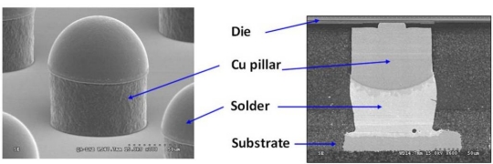
The tremendous interest in copper pillar (also called Cu pillar and copper post) was evident at ICEP with a standing-room-only crowd listening to ASE’s presentation on its plans for Cu pillar in FC-CSPs. Figure 1 shows the structure.

Click to Enlarge
Figure 1. ASE copper pillar structure.

ASE presented reliability data from test on a 5 × 5mm 65nm-technology die with 150µm bump pitch packaged in a 10 × 10mm package. ASE reported that it passed 3,000 hours of high temperature storage test at 150°C and 3,000 hours of thermal cycling test at -55 to +125°C. Results were also reported for a 40nm-technology 10 × 10mm die with 162µm bump pitch packaged in a 31 × 31mm form factor. The part passed 2,500 hours of -55 to +125°C thermal cycling test.

Wafer-level packaging (WLP)

Wafer level packaging remains a hot topic, with Hynix presenting its WLP developments for high-speed memory and ASE’s presentation on its fan-out packaging (FOWLP) for multi die.

Click to Enlarge
Figure 2. ASE FOWLP.

Figure 2 shows a fan-out package from ASE.

3D IC

3D packaging presentations were sprinkled throughout the conference. Many discussions in sessions and around the conference site focused on 3D TSV technology developments. A new test method to determine thin silicon die strength was presented by researchers from Chang Gung University in Taiwan. Researchers at ITRI presented their developments of wafer-level underfill bonding process for 3D chip stacking.

Too many package choices

With so many packaging choices, it has become difficult to select the appropriate package for the application. A presentation from IBM Japan proposed a methodology for packaging selection for mobile products. Choices included wire bond and flip chip chip scale packages (CSPs), quad flat pack no leads (QFNs), and WLPs (both conventional and fan-out).

Reliability matters

Reliability for all types of packages was discussed by many companies including Powertech Technology, Inc., Toshiba, NAMICs, Sanyu Rec, and Sony.

E.J. Vardaman is president and founder of TechSearch International, Inc. a company involved in analyzing technology and market trends in semiconductor packaging, materials and assembly since 1987. Learn more at www.techsearchinc.com

Subscribe to Solid State Technology/Advanced Packaging.

Follow Advanced Packaging on Twitter.com by clicking www.twitter.com/advpackaging. Or join our Facebook group

April 20, 2011 – Intel has handed out its annual supplier awards, this year to 28 companies, including some one-time "Achievement" awards for particular impact.

Click to Enlarge
(Image of statue from Intel.com)

To earn Intel’s "Supplier Continuous Quality Improvement" (SCQI) award — now in its 24th year — eight companies (vs. 10 honorees in 2009 and 16 in 2008) scored at least 95% on a list of performance and ability goals, including cost, quality, availability, delivery, technology and environmental/social/governance, over the past year. They also achieved ≥90% on an improvement plan and "demonstrated solid quality and business systems."

Another 20 suppliers (vs. 16 in 2009 and 26 in 2008) scored 80% or better to earn Intel’s 2010 "Preferred Quality Supplier" (PQS) recognition. Criteria include "consistently exceed[ing]" Intel expectations, aligning to technology and manufacturing roadmaps, meeting cost reduction goals, and delivering excellent "customer satisfaction." And this year, four suppliers were picked for an "Achievement Award," billed as a "one-time extraordinary achievement" that has "enabled significant business impact to Intel across the areas of cost, quality, availability, technology, sustainability and customer satisfaction."

"Our industry is experiencing significant changes that make it even more important to partner with outstanding suppliers to deliver leading-edge technology to our customers," noted said William Holt, SVP/GM of Intel’s Technology and Manufacturing Group, in a statement. "Continuous improvement is what differentiates good companies from great companies," added Brian Krzanich, SVP/GM of Intel’s Manufacturing and Supply Chain, and the eight SCQI winners excelled in "innovation, agility, customer responsiveness, and environmental sustainability."

More facts about this year’s inductees:

  • Disco, Hitachi High-Tech, Hitachi Kokusai, Senju, and Sumco are all threepeat SCQI winners. Fujifilm and Rofin-Baasel are three-time PQS winners.
  • TEL was the only supplier to climb up from last year’s PQS ranks into SCQI status.
  • Falling off last year’s SCQI list from a year ago: Daewon Semiconductor Packaging (now PQS status), DEK, Moses Lake/Tama Chemicals (also PQS status), Munters, and Verizon.
  • Gone from the PQS list: AceCo, ASE, Cisco, Nippon Mining & Metals, Nordson ASYMTEK, and Praxair Electronics. Grohmann and Hirata were PQS winners in 2009 but took home this year’s inaugural "achievement award."
  • Note that ASML and Nikon are both are still among Intel’s most recognized suppliers. Nikon used to be the incumbent litho tool supplier (and SCQI winner in 2008), but Intel is known to be splitting its litho business now with ASML — and with both suppliers recognized for a second year in a row, that plan seems to be working well.

Intel launched the SCQI program in 1987 to improve the systems and output of key suppliers, and minimize its time and money spent inspecting incoming material, goods, and services purchased. The company honored 26 companies in 2009, 40 in 2008, 48 in 2007, 54 in 2006, 38 in 2005, 43 in 2004, 45 in 2003, and 42 in 2002. (Note the trend of fewer companies being honored; the company didn’t say whether this is attributable to its own criteria, or to marketplace dynamics.)

The 2010 SCQI winners are:

* Disco (blade dicing and laser saws, wafer thinning, and polishing equipment)
* Hitachi High-Technologies (etching systems, FE-SEMs, CD-SEM, defect inspection tools)
* Hitachi Kokusai Electric (diffusion furnaces)
JSR (photoresists, packaging materials, and CMP consumables)
* Senju Metal Industry (electronic interconnect materials)
Shinko Electric Industries (plastic laminated packages and heat spreaders)
* SUMCO (200mm and 300mm polished and test silicon wafers)
** Tokyo Electron (semiconductor production equipment)

Winners of the 2010 PQS award include:

** ASML (lithography process tools)
** Cabot Microelectronics (CMP slurries)
* Daewon Semiconductor Packaging (handling media)
** Daifuku (fab automated material handling systems)
Dai Nippon Printing (advanced photomasks)
** Fujifilm Electronic Materials (chemistry, equipment for semiconductor device manufacturing)
Mitsubishi Gas Chemical (chemicals for semiconductor device manufacturing)
* Moses Lake Industries/TAMA Chemicals (ultrahigh-purity chemicals)
Murata Manufacturing (multilayer ceramic capacitors, inductors, and interference components)
** Nikon (lithography scanners and steppers)
** Rofin-Baasel (laser mark equipment)
Siltronic (polished and epitaxial silicon wafers)
STATS ChipPAC (turnkey packaging and test services)
Taiyo Yuden (multilayer ceramic capacitors, inductors, electromagnetic interference components)
TSMC (foundry services)

And the four suppliers named for one-time "achievement award" are:

Advantest (test equipment), for "velocity and availability"
Gemteck Technology (wireless products), for "customer satisfaction"
** Grohmann Engineering (assembly equipment), for "affordability"
** Hirata (automation equipment), for "breakthrough technology"

(* a 2009 SQCI winner)
(** a 2009 PQS winner)

April 19, 2011 — Multitest, a designer and manufacturer of final test handlers, contactors and load boards, announced that its ECON test contactor exceeded 4.5 million insertions at an Asian test house.

Click to EnlargeThe customer was able to run a high-volume application with more than 100k throughput per day at an octal-site set up for more than 1.5 years without contactor-wear related test cell downtime. The contactor performance resulted in a 99% stable test yield.

In this test cell set up, the overall performance also benefitted from the Multitest Plug & Yield program. The test house used the ECON together with the Multitest MT9928 test handler.

The ECON socket was launched for high-power applications of small size and small pitch devices (QFN). It also is available for SO, QFP and QFN packages with a lead pitches down to 0.25mm.

Multitest’s proprietary coatings ensure long life spans and high first pass yields. The high first pass yield results from a precise contact spring geometry and the use of a new type of plastic material that avoids thermal expansion. A high contact force of 0.45N per spring ensures repeatable electrical behavior. Additionally, the ECON socket is load-board compatible with existing RFC sockets and third party socket types. It also supports plunge-to-board applications in the full ambient-hot-cold temperature range.

Multitest designs and fabricates test equipment — contactors, boards and test handlers — for semiconductors. For more information, visit www.multitest.com.

Subscribe to Solid State Technology/Advanced Packaging.

Follow Advanced Packaging on Twitter.com by clicking www.twitter.com/advpackaging. Or join our Facebook group

April 19, 2011 – Marketwire — STATS ChipPAC Ltd. (SGX-ST: STATSChP), semiconductor test and advanced packaging service provider, is expanding its 300mm through silicon via (TSV) offering with the addition of mid-end manufacturing capabilities.

The TSV investment is the addition of a 300mm "mid-end" process flow that occurs between the wafer fabrication and back-end assembly process. Mid-end processes support the advanced manufacturing requirements of 2.5D and 3D TSV as well as wafer-level packaging (WLP), flip chip, and embedded die technology.

"We have had the capability to fabricate, assemble and test TSV interposers for four years and believe the timing is right to invest in 300mm mid-end TSV manufacturing for our customers," said Dr. Han Byung Joon, Executive Vice President and Chief Technology Officer, STATS ChipPAC.

Dr. Han continued, "Flip chip and wafer level packaging are important drivers of mid-end processing in addition to the anticipated growth in 3D solutions utilising TSV technology, particularly with the integration of memory and logic devices at advanced technology nodes. The initial markets that are expected to embrace 2.5D and 3D TSV technology are mobile applications and high performance processors for the computing segment. STATS ChipPAC will continue to invest and innovate in TSV technology to offer the next generation of 3D packages to our customers."

STATS ChipPAC was one of the first outsourced semiconductor assembly and test (OSAT) providers to invest in TSV technology with a 51,000 square foot research and development facility dedicated to the development of next-generation wafer-level integration with TSV technology.

TSV uses short vertical interconnections through a silicon wafer to achieve greater space efficiencies and higher interconnect densities than wire bonding and flip chip stacking. When combined with microbump bonding and advanced flip chip technology, TSV technology enables a higher level of functional integration and performance in a smaller form factor.

One of the first implementations of TSV technology is in the form of silicon interposers used to bridge 2D silicon designs into more advanced and efficient 3D configurations. Often referred to as the 2.5D technology, TSV interposers are an immediate and practical approach to die-level integration using the capabilities of TSV technology. TSV interposers provide flexibility for the integration of die from different technology nodes and deliver advantages in miniaturisation, thermal performance and fine line/width spacing in a semiconductor package.

STATS ChipPAC has complete front to back-end manufacturing capabilities for 200mm wafers and currently handles both chip-to-chip and chip-to-wafer assembly for TSV technology. This includes high-density microbump capabilities in solder and copper column materials, microbump bonding down to 40um pitch, thin wafer handling, wafer-level underfill, thin wafer dicing and microbumps for flip chip interconnection. Microbump technology is critical to delivering fine pitch, low profile solutions for high-performance devices.

STATS ChipPAC Ltd. is a service provider of semiconductor packaging design, assembly, test and distribution solutions in diverse end market applications including communications, digital consumer and computing. Further information is available at www.statschippac.com.

Subscribe to Solid State Technology/Advanced Packaging.

Follow Advanced Packaging on Twitter.com by clicking www.twitter.com/advpackaging. Or join our Facebook group

April 15, 2011 – PR Newswire — EoPlex Technologies Inc. is promoting the xLC substrate for quad flat pack no lead (QFN) semiconductor packages. The substrate enables QFNs with hundreds of leads and multiple rows at a lower cost than conventional packages.

The EoPlex xLC substrate is a sintered metal array of wire bond and die attach pads delivered on a temporary thin metal strip (the lead carrier). The product is designed to be a direct replacement for the leadframe and is completely compatible with all QFN processing. With EoPlex xLC, packages can be made with as many rows as needed with hundreds of leads. xLC production is based on sintering for better environmental friendliness.

QFNs are the fastest growing packaging segment; however, they cannot be used in many applications due to the limitations imposed by the metal leadframe that is used to build them. The most critical limitation is that the leadframe prevents multi-row and high-lead-count designs, which are currently served by BGAs, says EoPlex. The leadframe also makes QFNs bigger than necessary, adds extra metal that reduces electrical performance, requires expensive polyimide tape and can slow down process steps like dicing and testing.

By using space efficiently and adding no waste metal, the substrate allows up to 50% more package-sites on each strip, resulting in a price per package-site that is 20-30% less than leadframes, said Arthur L. Chait, CEO of EoPlex.

EoPlex is a private company backed by Draper Fisher Jurvetson, ATA Ventures, Labrador Ventures and Draper-Richards. More information is at www.eoplex.com.

Subscribe to Solid State Technology/Advanced Packaging.

Follow Advanced Packaging on Twitter.com by clicking www.twitter.com/advpackaging. Or join our Facebook group