Category Archives: Wafer Level Packaging

April 14, 2011 — E. Jan Vardaman, president and founder of TechSearch International, delivered a keynote address at the International Conference on Electronics Packaging (ICEP) held in Nara, Japan April 13-15. One of the key messages in her presentation was the trend toward the adoption of copper (Cu) pillar as highlighted in TechSearch International’s recent study, Flip Chip and WLP: Market Projections and New Developments.

Since Intel’s adoption of copper, many companies are moving to adopt copper pillar as the technology for their flip chip applications. Intel started with the use of copper pillar in its 65nm and 45nm flip chip product lines, and is using the technology in its 32nm products. The first products were the "Presler" and "Yonah" processors, but today Intel uses the copper pillar process in all of its flip chip products, including its Atom processor.

Cu pillar with a solder cap has also been used for GaAs and silicon in RF modules for several years. Amkor has been shipping RF Power Amplifier and RF front-end modules with Cu pillar bumps for more than four years. Drivers included size, performance, and cost.

Copper pillar is also shipping in leadframe packages from companies including Carsem and Unisem. IBM developed a copper pillar process called C2 that has been introduced for wire bond die with 50µm pitch or larger. TI has recently announced its use of Cu pillar in the bottom package of its package on package (PoP) offering.

Advantages of copper pillar, or copper post as it is sometimes called, were highlighted in TSMC’s recent technology day when TSMC presented its roadmap for the technology. Vardaman noted in her keynote that "the move to copper pillar is similar to the industry’s progression from the evaporated bump to the plated bump, and a major shift is expected in the 2013-14 timeframe."

Highlighted in the ICEP presentation was STATS ChipPAC’s low-cost FC-CSP based on copper columns, bond-on-lead interconnection, and molded underfill. A 20-40% lower cost over standard flip chip packages for most designs has been reported. Several subcontract assembly operations offer molded underfill, including Amkor, ASE, and STATS ChipPAC.

The tremendous interest in copper pillar was evident at ICEP with a standing-room-only crowd listening to ASE’s presentation on its plans for Cu pillar in FC-CSPs.

TechSearch International Inc. is market research firm specializing in technology trends microelectronics packaging and assembly. Learn more at http://www.techsearchinc.com

Subscribe to Solid State Technology/Advanced Packaging.

Follow Advanced Packaging on Twitter.com by clicking www.twitter.com/advpackaging. Or join our Facebook group

By Debra Vogler, senior technical editor

April 13, 2011 — New work from Stanford University goes beyond simple bump shear testing to allow simulation of stresses exerted on chips during semiconductor packaging. The researchers are able to explore how the stresses affect back-end structures.

Alex Hsing, a PhD student in Professor Reinhold Dauskardt’s Group at Stanford University, will be presenting a paper titled "Shear microprobing of chip-package interaction in advanced interconnect structures" at the IITC 2011 Conference (May 9-12, Dresden, Germany). In a podcast interview, Hsing summarizes the key results of the paper and explains how the group’s approach differs from simple bump shear testing.

Click to EnlargeListen to Hsing’s interview:  Download or Play Now

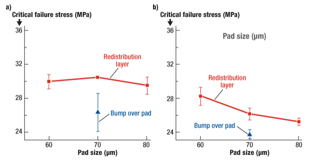
The researchers used a microprobe metrology system to evaluate advanced interconnect structures, studying a bump-over-pad design vs. an RDL design at three temperatures (room temperature, 50ºC, and 100ºC). At room temperature and 50ºC, the bump over pad design and the RDL design behave in a "relatively comparable manner." However, at 100ºC, the bump over pad design weakens significantly compared to the RDL design (see the figure). They concluded that the "comparatively lower temperature sensitivity of critical failure stress of the RDL design suggests that it may offer an advantage at high temperature," as noted in the paper. The group showed that shear stresses cause damage that can quickly propagate through multiple levels of metal.

Click to Enlarge

Figure. Critical failure stresses for the bump over pad design and the RDL design plotted as a function of pad size at 100ºC in the stronger direction (a), and in the weaker direction (b).

Hsing also addresses the anticipated "hot button" issues that will likely come up at the conference, and the next steps the researchers will take, (e.g., imaging methods will be needed to pair up with the metrology system described in the current paper).

Subscribe to Solid State Technology/Advanced Packaging.

Follow Solid State Technology on Twitter.com via editors Pete Singer, twitter.com/PetesTweetsPW and Debra Vogler, twitter.com/dvogler_PV_semi.

Or join our Facebook group

April 13, 2011 — Questar Products International, a manufacturer of automatic wire bonders for the global assembly market, released the Q7000 series of fine-pitch, fine-wire (17-75μm), aluminum/gold (Al/Au) automatic wedge and ball bonders to better meet smaller lot size, multiple product variation, frequent set-up change styles of package production.

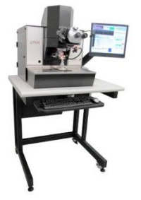
Click to EnlargeThe Q7000 Series has updated hardware and software, delivering a more tightly integrated assembly package, with approximately 30% fewer components and 50% less wiring than the Q2100 Series, which it replaces. These systems also cost less than the Q2100 models. The machines are designed with off-the-shelf components available directly from suppliers worldwide.

In addition, Questar has simplified the configuration selection process by including previously optional items, such as a programmable ultrasonic generator, as standard features.

Also standard is ball/stud bumping, stitch bonding, and table tear for wedge bonding. The customer chooses the appropriate heated or ambient workholder (and a programmable temperature controller if gold wire is to be used with the Q7800 wedge bonder) when ordering a Q7000 or Q7800 wire bonding system.

These automatic wire bonders support prototyping to medium-volume production. Designed for packaging applications from basic monolithic to complex hybrid devices and custom, specialty systems, the Q7000 series accommodates a multitude of device configurations. Package conversions are reportedly simple and can be completed in minutes.

The new design has also placed all control electronics on the top of the bonders for easier, no-tools-required access.

Questar Products offers hardware and software customization for specialty device applications such as unique wire-shaping and larger bondable area requirements.

Running on the Windows XP Pro operating system, the Q7000 Series offers intuitive, menu-driven software that is easy to program, with convenient access to all machine functions. The user-friendly operator interface provides point-and-click bonding; unlimited wires; easy bond process editing; extensive program storage; and a bond parameter library.

Questar provides wire-bonding machines to the global solid-state component assembly market. For more information on the Q7000 Series, visit www.questarproducts.com.

Subscribe to Solid State Technology/Advanced Packaging.

Follow Advanced Packaging on Twitter.com by clicking www.twitter.com/advpackaging. Or join our Facebook group

April 13, 2011 – ACN Newswire — Applied Materials Inc. (AMAT) manufacturing solutions provider to semiconductor, flat panel display and solar photovoltaic industries, signed an agreement with the Institute of Microelectronics (IME), a research institute under the Agency for Science, Technology and Research (A*STAR), to set up a Center of Excellence in Advanced Packaging in Singapore.

The Center will be located at Singapore’s Science Park II and will focus on developing new capabilities in advanced packaging, which is a key growth market for the semiconductor industry. The Center will have a full line of wafer level packaging (WLP) processing equipment for die stacking and through silicon vias (TSV), etc., and will conduct research in semiconductor hardware, process, and device structures. Applied has provided equipment for WLP since 2009 with a comprehensive line of processing systems for production line manufacturing.

Applied expects many advanced logic devices at the 40nm and below technology nodes to be packaged at the wafer level.

Russell Tham, regional president, Applied Materials South East Asia, said, "This collaboration is part of Applied Materials’ strategy to expand our global R&D network and extend our leading position in advanced packaging, bringing our development activities closer to our customers in Asia."

According to Professor Dim-Lee Kwong, Executive Director of IME, "Such a close collaboration will spur the growth of next generation equipment and translate into greater share of the semiconductor market in Asia and the world for Applied Materials, and position Singapore as the country of choice for global semiconductor R&D."

IME is a research institute with advanced R&D capabilities in 3D-ICs using TSV technology. IME’s capabilities in this area include its 300mm facility. The Center leverages R&D capabilities in 3D-TSV, built by IME over the years, to support advanced packaging tool development for Applied Materials, added Lim Chuan Poh, Chairman of A*STAR.

In April of last year, Applied Materials opened its Singapore Operations Center, its first facility in Asia for manufacturing advanced semiconductor equipment, at Changi North Industrial Park.

The ceremony for the planned Advanced Packaging Center was attended by Singapore’s Minister for Trade and Industry, Lim Hng Kiang.

Applied Materials, Inc. (Nasdaq:AMAT) provides innovative equipment, services and software to enable the manufacture of advanced semiconductor, flat panel display and solar photovoltaic products. Learn more at www.appliedmaterials.com.

The Institute of Microelectronics (IME) is a research institute of the Science and Engineering Research Council of the Agency for Science, Technology and Research (A*STAR). A*STAR oversees 14 biomedical sciences and physical sciences and engineering research institutes, and 9 consortia & centers. For more information about IME, please visit www.ime.a-star.edu.sg.

Subscribe to Solid State Technology/Advanced Packaging.

Follow Advanced Packaging on Twitter.com by clicking www.twitter.com/advpackaging. Or join our Facebook group

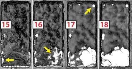
April 12, 2011 — Sonoscan, Inc., acoustic micro imaging systems maker, has demonstrated the single-scan imaging of a sample at 50 different depths, or gates. The technique, called PolyGate, yields 50 images that show internal features at each depth of the package.

In conventional imaging, much wider gates are used to confine imaging to a single depth of interest such as the die face or leadframe depth. The ability to set multiple gates that are imaged simultaneously during a single scan gives the system user the ability to see internal features at each gate, and to see how features, including defects, change from one gate to the next.

Click to Enlarge

Shown in the image are gates 15 through 18 (out of 50) imaging downward from the top surface of a ceramic chip capacitor that is 3.18mm thick. Each gate is about 60µm thick. PolyGate can set up to 200 gates, and Sonoscan has demonstrated 5µm gates in some materials.

Bright white regions in the acoustic image are defects. Small edge delaminations exist at Gate 15, but at Gate 16 a larger defective area appears in the lower right. In Gate 17 this area blossoms into a large delamination or void, and small voids appear at the top. The abruptness with which the large feature appears in Gates 17 and 18 suggests that the feature is very flat.

Sonoscan Inc. develops and manufactures acoustic microscopes and sophisticated acoustic micro imaging systems, widely used for nondestructive analysis of defects in industrial products and semiconductor devices. Sonoscan can be contacted at www.sonoscan.com.

Subscribe to Solid State Technology/Advanced Packaging.

Follow Advanced Packaging on Twitter.com by clicking www.twitter.com/advpackaging. Or join our Facebook group

April 11, 2011 — Yole Développement’s new report, "Flip-Chip: Technologies, Applications, Market report – April 2011" will be available at the end of April.

The report aims to provide an understanding of the new requirements and technologies that will reshape the supply chain of the world’s highest value package platform, flip chip.

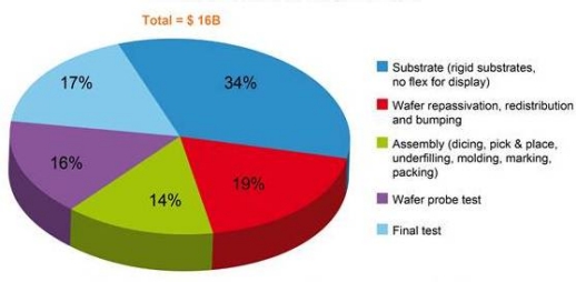
Flip-chip packages accounted for 13% of all integrated circuit (IC) packages by the end of 2010, but accounted for over 29% of the global IC assembly, packaging, and test market. Flip chip is a $16 billion market, and while it looks to be a large and mature packaging sector, Yole’s analysts argue that it is still in its growth phase, with major technology and application and supply chain transformations looming ahead.

Click to Enlarge
2010 total flip chip market value. Split by cost-of-ownership supply chain segments (substrates for LCD drivers excluded, service margin included). SOURCE: Flip Chip report, Yole Développement, April 2011.

Renewed interest in flip-chip technologies is motivated by the rising cost of gold used for wire bonding, the need for thinner devices, continued CMOS downscaling, higher currents and temperatures, and lower voltages.

Mobile applications are increasingly requiring footprint and weight reduction coupled with higher electrical performance (signal propagation and power distribution) that excludes wire bonded packages. The emergence of the 28nm CMOS technology node in particular poses new quality and reliability constraints on interconnect technologies, due to fragility, which may disqualify wire bonding. Increasing I/O density neccessitates new bumping

Companies cited in the report:

3M, AdvanPack Solutions, AEM Tec, Ajinomoto, Akita, Altera, AMD, Amkor, Apple, Applied Materials, ASE, Asymtek, Bergquist, Casio Micronics, Chipbond, Chipmos, Chomerics, Cookson, Datacon, Dek, Denka, Dow Chemical, Dow Corning, Elpida, EMMicroelectronics, Epcos, FCI, Fraunhofer IZM, Fuji Polymer, Fujitsu, Global Foundries, Henkel, Hitachi Chemical, Honeywell, Hynix, Ibiden, IBM, IC interconnect, IMI, Indium Corporation, Infineon, Intel, Ipdia, JCAP, J-devices, Kinsus, Kyocera, Laird Technologies, LB Semicon, Lord Corporation, Lumileds, Micrel, Minami, Murata, Namics, Nan Ya, Nepes, Nexx, Nichia, Nokia, Nordson, Nvidia, NXP, OKI, Omnivision, Optopac, OSE, Pactech, Panasonic, Polymatech, PowerTech (PTI), Premier Semiconductor Services, Qualcomm, Renesas, Samsung, Samsung Electromechanics (SEMCO), Shibuya, Shin Etsu, Shinko Electric, Siltech, Sony Chemical, Spil, StatsChipPac, ST-Ericsson, STMicroelectronics, Sumitomo, TDK, Tessera, Texas Instruments, Tong Hsing, Toray, Toshiba, Triquint, TSMC, UMC, Unimicron, Unisem, UTAC, Xilinx, Zymet.

and substrate technologies.

Flip-chip technologies and applications are diverse, with different drivers, levels of maturity, and sometimes alternative technologies. Flip-chip applies to a number of different applications addressing different packaging forms. To some, flip-chip applies to large digital system-on-chip (SOC) devices like microprocessors, graphical processor units or chipsets for personal computers and gaming stations. Flip-chip applies not only to packages but also to interconnection of bare integrated circuits, like the display drivers found around all LCD screens worldwide; and flip-chip packages can address devices with die sizes ranging from less than 1mm2 up to the maximum die sizes (around 650mm2).

The flip-chip market is undergoing major technology and supply chain transformations: emerging copper (Cu) pillar popularity, technology investments, changes to the supply chain, the role of CMOS foundries in flip chip packaging, and substrate cost/value. The Yole report describes their impacts on the semiconductor industry for the coming 5 years.

Key report highlights include the 2010 market status of wafer bumping for flip-chip, flip-chip package substrates, flip-chip underfills with breakdown of market data by player, player profile, region; Supply chain analysis and ranking of the wafer bumping, flip-chip substrate and underfills players; 2010 market status and 2011-2016 forecasts with breakdown by application area, IC type, bumping metallurgy in wafer counts and package units; the application fields of flip chips; copper pillar bumping status and developments; and more.

Access the report at http://www.i-micronews.com/reports/Flip-Chip/200/

Subscribe to Solid State Technology/Advanced Packaging.

Follow Advanced Packaging on Twitter.com by clicking www.twitter.com/advpackaging. Or join our Facebook group

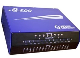
April 8, 2011 — Advanced Thermal Solutions, ATS, has released the iQ-200 thermal analysis system for precisely and simultaneously measuring the temperatures of solid materials and the surrounding air, as well as tracking air velocity and air pressure at multiple points to comprehensively profile heat sinks, components, and PCBs.

Click to EnlargeThe iQ-200 simultaneously captures data from up to 12 J-type thermocouples, 16 air temperature/velocity sensors, and 4 differential pressure sensors to analyze electronic packages.
The thermocouples provide surface area temperature measurements on heat sinks, components, housing parts and other locations to track heat flow or detect hot spots. Temperature data is recorded from -40 to +750°C. Air temperature and velocity are measured by up to 16 low-profile ATS candlestick sensors which can be placed throughout a system. Air temperature is tracked from 20 to 65°C and air velocity is measured from 0 to 6 m/s (1200 ft/min). The differential transducers capture pressure drop data along circuit cards, assemblies and orifice plates. Pressure measurements are taken from 0 to 0.15 psi (0 to 1,034 Pa).

iSTAGE application software manages the incoming data from multiple sensing devices, and provides rich graphic presentation on monitors and documents. The iQ-200 connects via USB to any conventional PC for convenient data management, storage and sharing. 

The iQ-200 can be factory modified at ATS to measure higher airflows, up to 50 M/s (10,000 ft/min), and air temperatures to 85°C.

Advanced Thermal Solutions is a leading engineering and manufacturing company supplying complete thermal and mechanical packaging solutions from analysis and testing to final production. Learn more at www.Qats.com

Subscribe to Solid State Technology/Advanced Packaging.

Follow Advanced Packaging on Twitter.com by clicking www.twitter.com/advpackaging. Or join our Facebook group

April 7, 2011 — Zymet Inc. introduced a reworkable edgebond adhesive, UA-2605, that improves thermal cycle performance of CBGAs and plastic BGAs.

In one trial, UA-2605 tripled the 0°C to +100°C performance of a CBGA, to nearly 2500 cycles. Previously, underfill was needed to achieve this level of performance, Zymet says.

Click to Enlarge
Figure 1. Edgebonded CBGA.

The edgebond adhesive is easier to process than an underfill. When applying underfill, the printed circuit board (PCB) is preheated to facilitate capillary flow, and multiple dispense passes are used to deposit sufficient material. With UA-2605, only four beads of the adhesive are required, one at each corner. There is no need to preheat the PCB, wait for underfill flow, and make multiple dispensing passes.

Click to Enlarge

Figure 2. After removal of underfilled BGA, underfill residues must be removed.

Reworking an underfilled BGA is a time consuming and delicate task. Underfill residues must be removed and, for fine-pitch BGAs, the risk of pad damage is high. With UA-2605, BGA rework is simple and straightforward. The temperature is raised and the adhesive is scraped away; then, the BGA is reflowed and lifted from the board. Little site cleaning is necessary.

Zymet is a manufacturer of microelectronic and electronic adhesives and encapsulants. Its products include die attach adhesives, substrate adhesives, UV curable glob top and cavity-fill encapsulants, and underfill encapsulants.

For more information, visit www.zymet.com.

Subscribe to Solid State Technology/Advanced Packaging.

Follow Advanced Packaging on Twitter.com by clicking www.twitter.com/advpackaging. Or join our Facebook group

April 7, 2011 – BUSINESS WIRE — Tessera Technologies Inc. (Nasdaq:TSRA – News) began two corporate initiatives to enhance the strategic positioning and value of its operations for its stockholders, customers and employees.

Tessera announced today the formation of a new group charged with developing, acquiring and monetizing semiconductor technologies beyond packaging, to be led by Simon McElrea. The group, which will be responsible for an initial portfolio of approximately 280 patents and patent applications, will consist of approximately 40 current employees located in San Jose. Their focus will be on circuitry design, memory modules, 3D architecture, and advanced interconnect technologies, among other areas.

Tessera also announced that it is exploring a possible separation of its Imaging & Optics business. As part of this initiative, Tessera has retained GCA Savvian Advisors, LLC as its financial advisor to assist in the evaluation of multiple alternatives, including, among others, a spin-off transaction.

"Our Imaging & Optics business has had a successful start. We believe under the leadership of its new president, Bob Roohparvar, it may grow more quickly and better serve its customers as a stand-alone entity, and we have begun the work of exploring alternative means to that end," added Nothhaft.

Tessera has not set a definitive timetable for completing its exploration of alternatives for the Imaging & Optics business and there can be no assurance that the process will result in any transaction. The company does not expect to make further public comment regarding these matters unless a definitive agreement or other commitment for any transaction is reached.

Tessera Technologies, Inc., develops, invests in, licenses and delivers innovative miniaturization technologies and products for next-generation electronic devices. Go to www.tessera.com.

Subscribe to Solid State Technology/Advanced Packaging.

Follow Advanced Packaging on Twitter.com by clicking www.twitter.com/advpackaging. Or join our Facebook group