Category Archives: Wafer Level Packaging

Kenneth A Ramsey,
Executive Vice President, MCT Worldwide, LLC, Minneapolis, MN USA

As IC’s get more powerful to meet consumer demand, and this same demand drives the prices ever lower, semiconductor device manufacturers are faced with one of the toughest challenges yet to emerge in their business. How do we continue to drive down the costs of these new chips when each new version becomes more complex to test and requires increasingly powerful testers? Over the past 10+ years, silicon designers have done a great job in adopting standards for their CAE tools. It is now possible to use "best-in-class" design tools because of the extensive use of standards among various CAE suppliers. Likewise, in the fabrication area, standards have played a large part in reducing the cost of building the chips. But when it comes to final production testing of the ICs, a lack of standards and the increasing complexity of the ICs being demanded by the marketplace has caused the cost-of-test to escalate, not decrease.

Studies have shown that packaging and test now account for, on average, about 50% of the total product cost for an IC; and this number is projected to rise to over 75% within the next few years. The rising cost of semiconductor device testing is now one of the main challenges to manufacturers. How are manufacturers addressing this new challenge? There are three major trends that are now emerging.

Strip testing allows devices to be production final tested in a massively parallel configuration while still in their leadframe or laminate array rather than one (or a few) at a time. The benefits have been proven in production by subcontractors and IDMs alike. Increased tester utilization of 10%-15%, higher first pass yields of 2%-4%, higher parallelism, far less jams and the ability to handle very small parts (3mmx3mm and below) are documented benefits of moving to strip testing over singulated testing. Strip testing is not for every device, but for those devices (and volumes) that make sense, strip test is a proven way to dramatically reduce the cost-of-test, often by as much as 40% or more.

Higher parallelism during testing of singulated devices is also becoming more widely used. While it clearly has benefits in some cases, it also suffers from the fact that high parallelism test handlers (either gravity or pick-and-place) for singulated parts are increasingly expensive compared to traditional singulated handlers and are still generally limited to parallelism of 32-up and below. Some manufacturers now report that their capex budget for "test" is now almost equally split between testers and test handlers. This is because testers are generally decreasing in cost while traditional singulated and pick-and-place test handlers are generally increasing in cost. This increasing cost for test handlers is due to a desire for higher parallelism and for the ability to handle ever decreasing device sizes.

Wafer probe has always been a key part of the IC testing process. Improvements in wafer probe with higher parallelism and increased accuracy have helped give rise to the concept of wafer-level packaging (WLP). In an effort to drive down the costs of a new device by eliminating the traditional plastic packaging, manufacturers are turning to WLP. In WLP, the device is singulated and then fully functionally tested, with higher levels of parallelism, at wafer probe and shipped to the customer for direct mounting on the PC board. The economics of WLP are rapidly approaching the point that makes it cost effective compared to traditional packaging.

We are seeing a dramatic change in how testing of ICs is accomplished. It’s no longer reasonable or feasible to expect that those old technologies will meet the demands of an increasingly complex and competitive industry. Higher parallelism, either for final packaged devices or for wafer level products, will be an indispensable part of any successful test organization, because it has been proven to drive down the cost-of-test.

Kenneth A Ramsey is EVP at MCT Worldwide, LLC, 121 South 8th Street, Suite #960,Minneapolis MN 55402 USA; (612) 436-3240.

Solid State Technology | Volume 54 | Issue 3 | March 2011

More Solid State Technology Current Issue Articles
More Solid State Technology Archives Issue Articles

February 28, 2011 — The new gold/tin (AuSn) process from Stellar Industries is ideally matched to Stellar’s proprietary CPU copper on aluminum nitride (AlN) submounts with its sharp guillotine edge for precise edge alignments.

Click to EnlargeThe new gold/tin process improves wettability and offers variable freeze time options to ensure efficient laser die bonding. Reduced micro-voiding improves thermal performance for increased reliability.

The AuSn performance is available from 70Au/30Sn to 80Au/20Sn compositions.

Learn more about this product at (508) 865-1668; [email protected]

Subscribe to Solid State Technology/Advanced Packaging.

Follow Advanced Packaging on Twitter.com by clicking www.twitter.com/advpackaging. Or join our Facebook group

February 24, 2011 — Multitest, a designer and manufacturer of final test handlers, contactors and load boards used by integrated device manufacturers (IDMs) and final test subcontractors, received its fifth full purchase order for its InCarrier device transfer system with InStrip test handling system adapted to metal frame-based carriers.

This new test handling process differs from traditional tube or tray loading of devices into gravity feed and pick-and-place systems. Instead, singulated devices are loaded into a patented micro-spring carrier frame that is handled on Multitest’s strip handling system.

With the InCarrier device transfer system, Multitest can achieve high test parallelism for singulated devices without compromising quality through post test singulation processing. The actual test handling is practically jam free, even for devices as small as QFN 2 x 2mm.

Multitest manufactures test equipment for semiconductors. Multitest markets test handlers, contactors, and ATE printed circuit boards. For more information about Multitest’s InCarrier, visit www.multitest.com/InCarrier.

Subscribe to Solid State Technology/Advanced Packaging.

Follow Advanced Packaging on Twitter.com by clicking www.twitter.com/advpackaging. Or join our Facebook group

February 24, 2011 – Business Wire — Nanometrics Incorporated (NASDAQ:NANO), advanced process control metrology system supplier, installed a next-gen UniFire 7900IR metrology system at a leading manufacturer of advanced logic devices. The Unifire 7900IR provides 3D inspection of wafer-scale packaging features as well as registration for wafer-to-wafer bonding applications for use in advanced wafer scale packaging process control.

"Careful control of lithography and etching in the through silicon via (TSV) flow, bumping, and wafer-to-wafer bonding processes is critical to enable high yielding devices for next generation advanced packaging. This latest system offers a new 3D inspection capability as well as an infrared (IR) microscope option, allowing direct measurement of features and structures in bonded wafer stacks," commented Dr. Michael Darwin, VP of the UniFire and Materials Characterization Groups at Nanometrics.

Existing UniFire systems can be field upgraded with both IR and 3D inspection options to further extend the capability of installed tools.

To learn more about the UniFire 7900IR and Nanometrics process control metrology solutions, visit Nanometrics at SPIE Advanced Lithography, San Jose Convention Center, March 1st-2nd.

Nanometrics provides advanced, high-performance process control metrology systems used primarily in the fabrication of semiconductors, high-brightness LEDs, data storage devices and solar photovoltaics. Nanometrics is traded on NASDAQ Global Select Market under the symbol NANO. Nanometrics’ website is http://www.nanometrics.com

Subscribe to Solid State Technology/Advanced Packaging.

Follow Advanced Packaging on Twitter.com by clicking www.twitter.com/advpackaging. Or join our Facebook group

February 21, 2011 – BUSINESS WIRE — Tessera Technologies Inc. (NASDAQ:TSRA) announced that on February 17, 2011, it sent Amkor Technology, Inc. an official notice of termination of their license agreement with Tessera. The two companies are currently in arbitration regarding multiple issues, including several past breaches by Amkor of the license agreement.

"We have concluded that the best course of action is to terminate Amkor’s license agreement with us," stated Henry R. Nothhaft, chairman and chief executive officer, Tessera. "We will take the necessary steps to protect our innovation and technology, our shareholders, and our licensees in good standing."

Tessera Technologies, Inc. invests in, licenses and delivers innovative miniaturization technologies for next-generation electronic devices. The company’s micro-electronics solutions enable smaller, higher-functionality devices through chip-scale, 3D and wafer-level packaging technology, as well as high-density substrate and silent air cooling technology. Learn more at http://tessera.com/Pages/tessera.aspx

Subscribe to Solid State Technology/Advanced Packaging.

Follow Advanced Packaging on Twitter.com by clicking www.twitter.com/advpackaging. Or join our Facebook group

By Debra Vogler, senior technical editor

February 18, 2011 — Jamal Izadian, co-founder & president of RFCONNEXT, made the case for shaped membrane transmission lines (SMTL) for use in high-speed 3D packaging applications, as guest speaker at a recent MEPTEC lunch forum (2/9/11, Santa Clara, CA). Observing that wire bonding is limiting high-speed performance and die stacking, and that high-speed digital signals are limited by traditional plastic packaging, he calls for SMTL use, in conjunction with two other solutions, called periodic micro transmission lines (PMTL) and via micro transmission lines (VMTL), as a total high-speed packaging interconnect solution.

Listen to Izadian speak: Download (iPhone/iPod users) or Play Now

Each of these technologies is described in a podcast interview with Izadian. He also explains how SMTL supports and improves flip-chip, micro-bumping, wafer thinning, system-in-package (SiP), package-on-package (PoP), and other packaging processes by extending the bandwidth and high-speed limits of these technologies.

An intriguing topic covered in the interview is Izadian’s contention that SMTL is an inexpensive PCB alternative solution to TSVs. Wire bonds are not transmission lines, so high-speed connectivity is not possible, observed Izadian. “With the advent of advanced transmission lines, which are almost as good as a coaxial line at the microscopic level, we have removed the requirement for the connections to be next to each other or on top of each other,” said Izadian. “You can have them dispersed around like a SiP and be able to connect them at high speed.” SMTL technology also allows plastic packaging to be used for high-speed applications, essentially obtaining the performance achieved with ceramic packages, but at a lower cost.  

Some of the advantages of SMTL include: controlled impedance, no parasitic inductance, no significant length limit, no cross-talk, noise immunity, 90% less metal in the process, and scalability.
 
SMTL for packaging applications is currently under evaluation by end users and RFCONNEXT intends to adapt the technology to existing manufacturing processes. Izadian said he expects advanced transmission lines to be ready within the next 6-12 months. Learn more at http://www.rfconnext.com/

Subscribe to Solid State Technology/Advanced Packaging.

Follow Advanced Packaging on Twitter.com by clicking www.twitter.com/advpackaging. Or join our Facebook group

February 17, 2011 – Marketwire — inTEST Corporation (NASDAQ: INTT), an independent designer, manufacturer and marketer of semiconductor automatic test equipment (ATE) interface solutions and temperature management products, announced that two INTT subsidiaries, Temptronic and Sigma Systems, both in Sharon, MA, will begin operating under the umbrella trade name, inTEST Thermal Solutions Corp.

Temptronic, established in 1970, and Sigma Systems, established in 1956, have come together to offer a line of thermal test products for test and process control. Effective immediately, customers, vendors, representatives and distributors of Temptronic and Sigma Systems will be conducting business with inTEST Thermal Solutions Corp. (www.inTESTthermal.com).

James Pelrin, president of inTEST Thermal Solutions Corp., noted, "This is the next step in the process of broadening the marketing range and engineering capabilities of the two separate entities. Together, Temptronic and Sigma Systems have been engineering and marketing leading-edge thermal solutions for over 100 years, solving unique and challenging temperature problems. Under the banner of inTEST Thermal Solutions Corporation, the division will engineer the broadest range of temperature-related test, conditioning, and process products on the market." Pelrin continued, "We specialize in meeting the most demanding applications by engineering unique thermal test solutions, whether it is a "non-standard" size, very specific and challenging transition rates, specialized access ports or temperature testing in a localized area. Our products include thermal chambers and platforms, air and fluid chillers, semiconductor test tools, and our unique mobile temperature test system."

The Thermal division product line addresses a number of growth markets, including high-speed networking and the use of fiber optic components and devices for 4G and 10G communications, broadband TV satellites, and military applications. Mr. Pelrin commented,

inTEST Corporation is an independent designer, manufacturer and marketer of ATE interface solutions and temperature management products, which are used by semiconductor manufacturers to perform final testing of integrated circuits (ICs) and wafers. For more information visit www.intest.com.

Subscribe to Solid State Technology/Advanced Packaging.

Follow Advanced Packaging on Twitter.com by clicking www.twitter.com/advpackaging. Or join our Facebook group

February 16, 2011 — STATS ChipPAC Ltd. (SGX-ST: STATSChP), semiconductor test and advanced packaging service provider, launched fcCuBE technology, an advanced flip chip packaging technology that features copper (Cu) column bumps, bond-on-lead (BOL) interconnection and enhanced assembly processes.

As semiconductor devices are scaled to advanced wafer technology nodes of 45/40nm and below, innovations in package structure, design and assembly process are key to achieving high performance, cost-effective product solutions. fcCuBE technology delivers high input/output (I/O) density, high performance and superior reliability in advanced silicon nodes, according to the company. It enables flip chip packaging with a 20-40% lower cost than standard flip chips. Benefits of the new flip chip technology include high I/O escape routing density, scalability to very fine bump pitches of 80 micron and below with finer effective pitches, significant reduction of stress on ultra low-k (ELK/ULK) structures that has been proven down to 45/40 nanometer (nm) and 28nm silicon structures, broad fab node compatibility, higher resistance to electromigration, lead-free materials, and lower cost.

fcCuBE technology is based on STATS ChipPAC’s proprietary BOL interconnect structure, which has been combined with Cu column bump to deliver an ultra-high I/O escape routing density with a finer bump pitch compared to standard solder bumps. The advancement enables more relaxed substrate design rules than standard flip chip packaging and provides scalability to very fine bump pitches.

Although copper is a harder bump material that can cause damage to ELK/ULK layers in finer silicon nodes, STATS ChipPAC has completed extensive thermo-mechanical simulation testing on fcCuBE technology with results demonstrating a significant reduction of stress on ELK/ULK structures, consistent with empirical data generated with 45/40nm as well as 28nm node product test vehicles.

"We are seamlessly deploying the core fcCuBE technology beyond traditional single-die flip chip packaging into more complex stacked/3D packages including Package-on-Package (PoP), Package-in-Package (PiP), flip chip/wire bond hybrid packages and next-generation Through Silicon Via (TSV) configurations," noted Dr. Han Byung Joon, EVP and CTO, STATS ChipPAC.

The fcCuBE will suit end products in the mobile/handheld, computing and high-end network/telecom markets, added Dr. Raj Pendse, STATS ChipPAC VP of product and technology marketing.

STATS ChipPAC Ltd. provides semiconductor packaging design, assembly, test and distribution solutions in diverse end market applications including communications, digital consumer and computing. Further information is available at www.statschippac.com

.Subscribe to Solid State Technology/Advanced Packaging.

Follow Advanced Packaging on Twitter.com by clicking www.twitter.com/advpackaging. Or join our Facebook group

February 15, 2011 – Marketwire — InVisage Technologies Inc., image sensor technology start-up, received its series C round of venture funding, led by Intel Capital. The undisclosed amount will be used to bring the company’s quantum-dot-based QuantumFilm technology and products into mass production.

Intel Capital joins InVisage’s existing investors RockPort Capital, InterWest Partners, OnPoint Technologies and Charles River Ventures.

QuantumFilm was developed by InVisage after research at the University of Toronto and at InVisage. The technology is based on quantum dots — semiconductors with unique light-capture properties. QuantumFilm works by capturing an imprint of a light image, and then using the silicon beneath it to read out the image and turn it into versatile digital signals. InVisage spent three years engineering the quantum dot material to produce highly sensitive image sensors that integrate with standard CMOS manufacturing processes.

The first application of QuantumFilm will enable high performance in tiny form factors, breaking silicon’s inherent performance-resolution tradeoff. Initially targeting cameraphone applications, which is the largest and fastest growing portion of the image sensor market, InVisage Technologies’ QuantumFilm will be sampling by summer, and could be in devices early next year.

"Image sensors for smart phones and handheld devices are a huge market opportunity and InVisage is well positioned to capture significant market share," says Dave Flanagan, managing director, Intel Capital. "InVisage is the first company in a while to think differently about image sensors and we are confident that its products will lead the imaging market on a new vector of innovation."

"The image sensor industry as a whole has focused entirely on increasing the number of pixels and has failed to see the big picture. As a result, there has been a lack of new ideas in the market for some time," says Jess Lee, CEO, InVisage Technologies. "InVisage’s QuantumFilm technology will bring stunning image quality and advanced new features."

InVisage Technologies, Inc. is a venture-backed fabless semiconductor company developing imaging-sensing technology that will replace silicon. More information is available at www.invisage.com.

Subscribe to Solid State Technology/Advanced Packaging.

Follow Advanced Packaging on Twitter.com by clicking www.twitter.com/advpackaging. Or join our Facebook group

By Dave Rose, Keithley Instruments, Inc.

February 14, 2011 — Thorough characterization of any material or device requires precision DC, AC impedance, and ultra-fast I-V or pulsed I-V measurements. Test equipment connection to a semiautomatic or manual probe station can be complicated. If performed incorrectly, it could diminish on-wafer measurement accuracy. This article addresses specific cabling techniques for DC, multi-frequency capacitance, and ultra-fast I-V and pulse testing, as well as the importance of proper grounding and shielding, choosing the proper interconnect for a specific measurement, and troubleshooting common interconnect problems.

Cabling for DC measurements: Potential error sources

Understanding anticipated measurement levels makes it easier to assess potential error sources. For simplicity, let’s assume that all of the signals being measured are neither high voltage (i.e., greater than 100V) or high current (greater than 200mA). We can break down the error sources into three categories: leakage currents, electrostatic interference, and mechanical effects.

Leakage currents. Leakage currents are currents flowing through paths other than the intended signal paths, for example, current flowing through the interconnect insulator. This leakage current can be a problem when the device under test (DUT) impedance is similar to that of the various insulators in the circuit. The simplest fix is to use a high quality cable with a high resistance insulator such as Teflon or polyethylene. Better cables can often reduce the effects of dielectric absorption, which is also a function of the insulator material.
Click to Enlarge
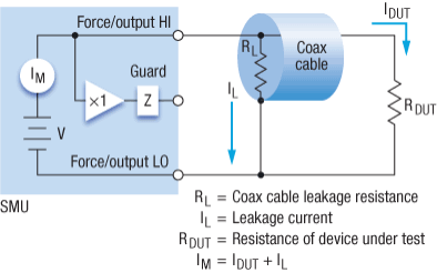
Figure 1. Leakage current flows through the cable’s insulation resistance.

Although using quality cables can go a long way toward reducing leakage currents, it may not always be sufficient. It’s important to understand what happens when a typical DC instrument, such as a source-measure unit (SMU), is connected to the DUT using a coaxial cable. In Figure 1, a leakage current (IL) flows through the cable’s insulation resistance (RL). This causes the SMU to measure the sum of the current flowing through the DUT (IDUT) and the leakage current, rather than just the current flowing through the device.

Guarding can eliminate the effects of leakage currents flowing through the insulator. A guard is a low-impedance point in the circuit that’s at the same potential as the high-impedance lead in the circuit. In a guarded measurement, because the shield is driven to the same potential as the force high terminal of the SMU, no current flows through the insulation resistance, eliminating leakage current effects.
Click to Enlarge
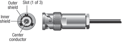
Figure 2. Triaxial cable

Guarding requires a third connection on the test instrument in addition to the shield and signal conductor. Although it’s theoretically possible to use a guarded connection on a coaxial cable, it would be unsafe because the shield would be at the same potential as the force terminal. The SMU guard should never be connected to the shield of a coaxial cable. However, using a triaxial cable solves this problem because it has two shields: an inner shield to which the guard is connected, and an outer shield that is connected to low terminal (Figure 2).

Electrostatic and magnetic interference. These kinds of interference occur when electrically (or magnetically) charged objects disturb the circuit under test. Although these effects are negligible at low impedances because the charges dissipate quickly, that doesn’t hold true at high impedances. Typically, electrostatic interference sources are environmental, such as fluorescent lights, motors, and even people. Electrostatic interference-induced errors are generally due to some type of capacitive coupling into the circuit, which can create an extra current defined by this equation: Click to Enlarge

Errors due to electrostatic coupling can be minimized in two ways. The first is to use shielded triaxial cables. Another is to connect the prober’s head plate, dark box, or metal enclosure to ground, so the induced current noise will flow through the shield to ground and not through the DUT.

Although grounding the prober’s enclosure or head plate is a good way to reduce electrostatic interference, doing it poorly can make matters worse. Typically, the prober and instrument are connected to two separate power line grounds because they are usually connected to separate power outlets. In that set up, a fluctuating current can flow between the instrument and the probe station, causing the instrument’s ground unit or low connection to move, producing errors. These are known as ground loops; to prevent them, the prober enclosures and shield should be connected to a common point.

Mechanical effects. Triboelectric and piezoelectric effects are also significant sources of DC measurement errors. Triboelectric currents are generated by charges created by friction between a conductor and insulator: free electrons are rubbed off the conductor, creating a current charge imbalance that generates current flow. This effect is noticeable when low quality cables are flexed. The insulators of high-quality cables are usually coated with a lubricating layer of graphite, which minimizes friction. Even high-quality triax cables need vibration isolation, which can cause some current flow due to piezoelectric effects. Placing a prober on an air table and using remote pre-amps to minimize the triax cables’ length can help minimize these problems.
Click to Enlarge
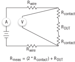
Figure 3. Kelvin (four wire) connection

Losses due to two-wire connections. No matter how good the cable is, losses through it can still be significant. The resistance of most interconnect cables is only a few ohms for even a very long length of cable. However, when the resistance of the DUT is also relatively low (e.g., a metal structure), and the instrument is connected to the DUT using two-wire connections, the resistances contributed by the cables and pad contacts can cause large errors. For example, if the resistance of the cables, contacts, and DUT are single ohms, then the meter will measure the sum of these resistances. Fortunately, four-wire or Kelvin connections (Fig. 3) offer a way to solve losses due to drops across the interconnect. In a Kelvin connection arrangement, a voltmeter is connected across the DUT. The instrument can force current and measure the voltage drop across the DUT. In this case, given that the voltmeter has a high impedance, very little current will divert to the voltmeter. Therefore, the forced current is essentially the same at all points in the circuit and the voltmeter will measure only the voltage drop across the DUT plus the contact resistance, not the resistance of the interconnect cables.

Cabling for C-V measurements: Potential error sources

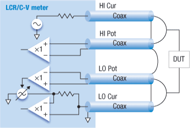
Semiconductor capacitance (C-V) measurements are typically performed using a multi-frequency capacitance meter (Fig. 4) with four terminals: high current (HI Cur), high potential (HI Pot), low current (LO Cur), and low potential (LO Pot). These terminals are coaxial, so they normally require a coaxial interconnect cable. They also have a fixed characteristic impedance, typically 50 or 100ohm. A multi-frequency capacitance meter measures impedance by sourcing a small AC voltage across the DUT and measuring the resulting AC current and AC voltage.
Click to Enlarge
Figure 4. Multi-frequency capacitance meter with 4 terminals.

The signals used to measure capacitance are AC, so take care that the signal paths minimize impedance changes. Changes will generate signal reflections that can impact the AC source and measure signals, causing erroneous readings. A good technique is to use cables with the same characteristic impedance as the instrument. Also, most capacitance meters perform some form of cable compensation, which involves entering the cables’ lengths into the meter set up. All four cables must be the same length to minimize impedance changes in the signal path and ensure the meter’s cable compensation calculations are correct.

Improperly shielded coaxial cables can also cause errors in capacitance measurements, so check that the cables’ shields are not open.

Stray cabling and interconnect inductances can cause resonances in the test circuit, producing erroneous capacitance measurements. Reduce the inductance by connecting the shields of the coaxial cables as closely as possible to the DUT, isolating the inductance from the measurement.

Cabling challenges for ultra-fast DC and pulse measurements

These measurements involve signals in the AC or high-frequency domain, which requires a different approach and considerations than for DC or C-V measurements.

Fourier series analysis shows that, no matter the speed of a pulse, it can be modeled as a series of sinusoids of varying amplitudes and frequencies. If the signal path can’t pass higher frequencies accurately, some fundamental frequencies are affected, distorting the shape of the pulse and affecting the power transmitted to the device. Therefore, pulse testing requires a signal path with a higher bandwidth requirement (approximately 150MHz) than either DC or C-V testing.

Pulse generators don’t typically include measurement capabilities, and oscilloscopes don’t source. The connections are single-ended; the center conductor carries the signal and is connected to the DUT. The shield of the coaxial cable is the return path for the signal and ideally should be connected to the low terminal of the DUT. A new class of pulse instruments does offer measurement capabilities, but even these instruments use a single coaxial cable to the probes for each channel. To prevent reflections, the interconnect’s impedance should match that of the source. Most pulsing instruments have a 50ohm input impedance, so one normally uses 50ohm coaxial cables to connect to the instrument. To minimize inductances, it is a good practice to connect the shields of multiple coax cables together.

To ensure the entire signal path is free of impedance changes or insertion losses, ideally, the shield of the coaxial cable should be connected to the low side of the test circuit. And while connecting the low side of the DUT to DC ground will work, the return signal now may follow two paths back to the instrument: one through earth and the second through capacitive coupling to the coaxial shield. Connecting the low side of the test circuit to a DC return path will ultimately limit the fidelity of the pulse. 

DC I-V measurements:

  • Triaxial cables
  • Kelvin connections
  • Isolated, driven guards


LCR/C-V measurements:

  • Coaxial cables
  • Kelvin connections
  • Shields connected at the probe tips
  • Impedance of cables needs to match the input impedance of the instrument


Pulsed I-V measurements:

  • Coaxial cables
  • Non-Kelvin (single cable) connection
  • Shields connected near the probe tip
  • Impedance of cables needs to match the input impedance of the instrument

Different measurements; different cabling requirements

As the table outlines, each measurement type has its own cabling requirements. Testers must change the prober cabling between DC I-V, C-V, and pulse testing on a DUT, especially if no switch matrix is being used. Changing cables can be time-consuming and often requires raising and lowering the probes between tests, which risks damaging the wafer pads. A new multi-measurement prober cables (MMPC) kit optimized for use with Suss and Cascade probers offers a simple solution to this problem and supports I-V, C-V, and pulsed measurements using a single set of triax interconnects. Keithley’s MMPC cables are special triaxial cables and adaptors that allow both high-precision DC and high-bandwidth AC connections to the probes and DUT. The cables can be arranged in Kelvin and non-Kelvin configurations. Set-up can be done without disturbing the cabling to the probes; only the cables at the prober connector bulkhead are moved. Keithley’s Model 4225-RPM Remote Amplifier/Switch, a companion to Keithley’s 4225-PMU Ultra-Fast I-V Module, automates reconfiguring MMPC cables when using the Model 4200-SCS Semiconductor Characterization System.

Dave Rose is senior staff applications engineer, Keithley Instruments Inc. Contact him at ph. 440-498-3040; [email protected]; Keithley Instruments, Inc., 28775 Aurora Road, Cleveland, OH 44139. For details on the transmission line concepts that underlie this interconnect approach, download a copy of Keithley’s white paper on the topic, "Labs’ Demands for Greater Measurement Flexibility Require Cabling Systems Capable of Accommodating Multiple Measurement Types," available at http://www.keithley.com/data?asset=52554.

Subscribe to Solid State Technology/Advanced Packaging.

Follow Advanced Packaging on Twitter.com by clicking www.twitter.com/advpackaging. Or join our Facebook group