Category Archives: Wafer Level Packaging


By Debra Vogler, senior technical editor

January 31, 2011 — Arthur Chait, president and CEO of EoPlex, describes the company’s high-volume print forming technology — a lead carrier product called xLC– and how it enables a cost-effective replacement for conventional quad flat pack no-lead (QFN) leadframes.

Listen to Chait’s interview: Download (for iPhone/iPod users) or Play Now

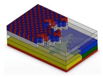
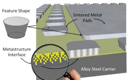
In a podcast interview with Debra Vogler, senior technical editor, Chait explains how a 3D structure is built up "microbrick" by microbrick using 3D pixels, called voxels (volumetric pixel), that are addressable (i.e., able to be changed) (Fig. 1). Key to the technology is being able to control the feature shape and metastructure interface (Fig. 2), which Chait discusses in detail in the podcast.

Click to Enlarge

Figure 1. EoPlex model (used as an example) showing different materials (colors) and different metastructures (patterns).

By using high-volume print forming, the resulting lead carrier lowers costs (compared to QFN leadframes) by minimizing the amount of metal needed for the structure and eliminating the need for processes such as plating and etching. The company is currently working with potential customers to evaluate and qualify the xLC product; qualification testing is expected to be completed sometime in the second or third quarter of this year and Chait says the company expects to be in full production by the end of 2011.

Click to Enlarge

Figure 2. Two keys to the success of the xLC are controlling the feature shape and engineering the metastructure interface.

Follow Advanced Packaging on Twitter.com by clicking www.twitter.com/advpackaging. Or join our Facebook group

January 27, 2011 — A fast-cure, low-shrinkage adhesive for optics and optical assembly, DYMAX OP-67-LS opto-mechanical adhesive cures in seconds for bonding of optical components. The product’s low-shrink nature virtually eliminates movement during curing and subsequent thermal cycling.

OP-67-LS offers the ability to "cure on demand" with exposure to longwave UV and visible light, allowing maximum flexibility in positioning parts prior to cure. OP-67-LS features 0.2% linear shrinkage upon cure.

OP-67-LS offers superior moisture resistance, very low outgassing, and adhesion to a variety of substrates including metal, glass, ceramic and polycarbonate, allowing its use in many critical and demanding applications such as fibre-optic "V" groove bonding, positioning laser diodes, fibre pig tailing, transceiver potting, VCSEL positioning and mounting active devices, or passive couplers, prisms and other optical device assemblies.

Also read: Device-level packaging for optical integration by Gilbert Lecarpentier (SUSS) and Livia Racz (AXSUN)

Learn more at http://www.intertronics.co.uk/products/lensbond.htm

Subscribe to Solid State Technology/Advanced Packaging.

Follow Advanced Packaging on Twitter.com by clicking www.twitter.com/advpackaging. Or join our Facebook group

January 25, 2011 – BUSINESS WIRE Tessera Technologies Inc. (Nasdaq:TSRA) announced that Bruce McWilliams, PhD, chief executive officer of SuVolta, Inc., has resigned as a member of Tessera’s board of directors effective immediately, to devote his time and attention to the needs of SuVolta’s growing business.

"Bruce has been a valuable contributor to Tessera, both as a member of our board and as our former chief executive officer," said Tessera’s chairman and chief executive officer Henry R. Nothhaft. "His leadership and insight have been great assets to Tessera, and I would like to thank him for many years of dedicated service."

McWilliams joined Tessera’s board of directors in June 1999, and he served as the company’s president and chief executive officer from June 1999 to July 2008 and as the company’s chief strategy officer from August 2008 to April 2009.

"It has been personally and professionally gratifying to work with Tessera," McWilliams said. "I look forward to following the company’s progress, and I wish the entire Tessera team the very best."

The company is currently conducting a search for his replacement.

Tessera Technologies Inc. invests in, licenses and delivers innovative miniaturization technologies that transform next-generation electronic devices. For information go to www.tessera.com.

Subscribe to Solid State Technology/Advanced Packaging.

Follow Advanced Packaging on Twitter.com by clicking www.twitter.com/advpackaging. Or join our Facebook group

January 24, 2011 — Semiconductor Research Corporation (SRC) and researchers from Stanford University have developed a combination of elements that yields a unique nanostructure material for packaging. This advance should allow longer life for semiconductor devices while costing less than current state-of-the-art materials. In addition to chip manufacturers, several other industries could also gain greater product efficiencies from related thermal energy management technology.

Semiconductor manufacturers currently rely on tiny pins or thick solder to bond sections of the semiconductor in order for the device to perform. However, current solder materials tend to degrade and fail due to heat and mechanical stress. To continue the scaling of integrated circuits (ICs), SRC and Stanford have researched materials that provide a high thermal connectivity (comparable to copper) with the flexible compliance of foam. The answer has been created through a nanostructured thermal tape that conducts heat like a metal while allowing the neighboring materials to expand and contract with temperature changes (metals are too stiff to allow this). This ability to reduce chip temperatures while remaining compliant is a key breakthrough for electronic packaging.  

"A big roadblock to increasing the performance of modern chips is hot spots, or millimeter-sized regions of high power generation. This advance in nanostructured materials and methods will allow us to better cool these spots and serves as a key enabler for densification of computational circuitry," said Professor Ken Goodson, lead researcher for SRC at Stanford University. "This can help packaging to withstand the demands of Moore’s Law."

In addressing the challenges of miniaturization, the first line of defense for hot spots is the interface material. Incorporating nearly two decades of advanced research and simulations for problems at the packaging level — much of it funded by SRC — the Stanford team ultimately arrived at their unique combination of binder materials surrounding carbon nanotubes (CNTs). The researchers expect it to facilitate the highest thermal conduction and the most desirable level of elasticity of any known packaging solutions.

"This new thermal nanotape revolutionizes the chip’s heat sink contact," said Jon Candelaria, director of Interconnect and Packaging Sciences at SRC. "Instead of being forced to rely upon the properties of just a single material, this combination gives the integrated circuits industry an opportunity to circumvent severe performance limitations and continue to improve packaging without adding cost."

While the research was funded by members of SRC to enhance computer chips, demand for applications of this kind of thermal interface also is rising in other industries. For instance, several automotive-related companies hope to recover electrical power from hot exhaust gases in cars and trucks using thermoelectric energy converters but reliable interfaces are a problem. Professor Goodson leads a major grant from the National Science Foundation (NSF) Department of Energy Partnership on Thermoelectric Devices for Vehicle Applications, with the goal of transferring the SRC-funded interface work to vehicles.

Patents for the technology are pending. The next step in the research is to license the new methods and materials to advanced thermal-interface companies for application tailoring and commercialization. End users are expected to benefit from the technology by 2014.

For more information and details about the new packaging materials and methods, visit http://pubs.acs.org/doi/abs/10.1021/nl100443x and http://microheat.stanford.edu/publications/A119.pdf.

SRC is a university-research consortium for semiconductors and related technologies that defines industry needs, invests in, and manages the research that gives its members a competitive advantage in the dynamic global marketplace. For more information, visit www.src.org.

January 21, 2011 — In a move that promises to provide increased performance and smaller size for portable electronics and other advanced systems, CEA-Leti signed a multiyear agreement with SHINKO ELECTRIC INDUSTRIES CO. LTD. to develop advanced semiconductor packaging technology. They will focus on volume production of silicon interposers.

The work, which will be part of Leti’s broader efforts in advanced silicon substrates, will focus on silicon interposers, a technology that has existed for some time but that now offers a number of compelling advantages for next-generation applications. These passive intermediate layers can be used in several ways to boost the useable performance and reduce the footprint of advanced silicon chips, providing much of the benefit of 3D packaging without requiring wholesale changes to design and manufacturing processes.

Example applications include the mounting of multiple chips on a single interposer, and the use of interposers to route large numbers of input/output connections onto silicon dies that would otherwise be too small to accommodate them.

Engineers from SHINKO, headquartered in Nagano, Japan, will work alongside Leti personnel at the common lab, which will be located at Leti’s headquarters facility in Grenoble, France. Leti provides world-class facilities and expertise for experimentation and evaluation, plus the ability to integrate new technologies into existing high-volume manufacturing flows.

"This collaboration will combine the intelligence and creativity of fine technical staffs, and we expect the resulting advances to be quickly adopted into real-world applications," said Laurent Malier, CEO of Leti. "SHINKO has done the preceding development of the processing 3D silicon packaging technologies so far. SHINKO can accelerate development for mass production of the next-generation high-density substrate by the joint development with Leti," added Mitsuharu Shimizu, senior corporate officer of SHINKO.

CEA is a French research and technology public organization, with activities in four main areas: energy, information technologies, healthcare technologies and defence and security. Within CEA, the Laboratory for Electronics & Information Technology (CEA-Leti) works with companies in order to increase their competitiveness through technological innovation and transfers. CEA-Leti is focused on micro and nanotechnologies and their applications, from wireless devices and systems, to biology and healthcare or photonics. Nanoelectronics and microsystems (MEMS) are at the core of its activities. For more information, visit www.leti.fr.

SHINKO is an all-around manufacturer of semiconductor packages, notably lead frame and Plastic Laminated Packages (PLP). More information on SHINKO is available at http://www.shinko.co.jp/english/index.html

Subscribe to Solid State Technology/Advanced Packaging.

Follow Advanced Packaging on Twitter.com by clicking www.twitter.com/advpackaging. Or join our Facebook group

January 20, 2011 — Brush Engineered Materials Inc. (NYSE:BW) will change its name to Materion Corporation (NYSE:MTRN) and unify all of its businesses under the new name effective March 8, 2011. The Company’s common stock will continue to trade on the New York Stock Exchange. Concurrent with the March 8 name change, the Company also will unveil a new company website and company-wide brand identity.

Brush Engineered Materials began in the metals, mining and specialty metals businesses, but has evolved into other areas like thin-film solar and microelectronics packaging materials, said Richard J. Hipple, chairman, president and CEO. He added that "heritage" businesses are very successful and integral to the company’s future, part of a much larger portfolio. "Through changes, acquisitions and other internal initiatives, we have expanded into a brand new 80-year-old company at the forefront of technologies essential to our customers. We are a leading global producer of advanced materials and services providing enabling technology solutions for customers in the fastest-growing segments of long-term global growth markets, including consumer electronics, telecom infrastructure, defense and science, industrial and commercial aerospace, energy and medical."

"As we have grown, our businesses continued to operate under original names and brand identities. That has made it difficult to position the Company as a single, unified organization. We find that even some long-time customers are not aware of the full scope of our capabilities."

Hipple added, "We are often competing against large global players that enjoy strong brand recognition. With annual sales of more than $1.2 billion and growing at a compounded annual growth rate of 17% since 2002, we have the resources and critical mass to participate successfully at that level. We expect to benefit from the recognition that comes from one name and a single strong brand."

In its transformation, Hipple noted that the Company has also become leaner, faster-growing, more diversified, and less cyclical. "We have a higher-value business model today in terms of our growth potential, margins, cash flow, balance sheet and capital structure. We believe the new name will better reflect the new Company."

The unification of all of the Company’s businesses under the Materion name is intended to create efficiencies and facilitate synergies. The new name, along with a new business unit alignment under the Materion brand, is expected to provide customers with better access and recognition to a broader scope of products, technology and value-added services.

Brush Engineered Materials Inc., through its wholly-owned subsidiaries, supplies highly engineered advanced enabling materials to global markets. Products include precious and non-precious specialty metals, inorganic chemicals and powders, specialty coatings, specialty engineered beryllium alloys, beryllium and beryllium composites, and engineered clad and plated metal systems. http://www.beminc.com/ Subsidiaries: Brush Wellman Inc.; Williams Advanced Materials Inc.; Technical Materials, Inc.; Zentrix Technologies Inc.; Brush Ceramic Products Inc.; Beryllium Products

Williams Advanced Materials supplies specialty materials used in thin film deposition and semiconductor packaging applications. Learn more about Williams Advanced Materials (WAM) at http://www.williams-adv.com/

 Subscribe to Solid State Technology/Advanced Packaging.

Follow Advanced Packaging on Twitter.com by clicking www.twitter.com/advpackaging. Or join our Facebook group

by Dr. Phil Garrou, contributing editor

January 19, 2011 – 2011 will the next update of the International Technology Roadmap for Semiconductors (ITRS) Assembly and Packaging Roadmap. (The 2009 ITRS was summarized here and the full report can be can be accessed here.

2009 was the first Roadmap where 3D integration became an important and integral part of both the Interconnect and the Assembly & Packaging sections.

In his keynote address at the MEPTEC Semiconductor Packaging Roadmaps conference, Bill Bottoms, co-chairman of the ITRS assembly and packaging technical working group (TWG), revealed several topics that will undergo expanded coverage in the 2011 roadmaps:

Medical electronics

  • Implantable medical electronics (Parkinson’s disease symptom control)
  • Selected issues for medical electronics:
    – Power requirements (energy scavenging, wireless radiated power, batteries)
    – Safety issues (voltage, biocompatibility, power delivery)
    – FDA certification
    – Reliability requirements
    – Environmental issues
    – Connectivity (wireless)
    – Optical components (cameras)
    – Microfluidics
    – Implantable micro-robotics
    – Sensors
    MEMS

3D integration

  • Thermal management for 3D structures
  • Power integrity
  • 3D SiP
  • Co-design and simulation

Interposers

  • Systems integration for 2D and 3D
  • Interposer features: redistribution wiring, passive networks, thermal management, stress management

Thin wafer & die handling

  • Testing: contactors with ohmic contact without damage
  • Holding mechanisms: Vacuum chucks (porous ceramic chucks), temporary bonding (sacrificial layer), electrostatic chucks, Bernouilli chuck
  • Dicing of thin wafer
  • Warpage

Embedded components:

  • Performance enhancement due to reduced distance between die and passives
  • Incorporation of additional functionality (heat pipes; wave guides)
  • Keep out area around embedded components
  • Charge source close to the die for current surge
  • Reduced size by placement of passives under die
  • Placement accuracy for small thinned die
  • 3D alignment tolerance for assembly
  • Improved resistance to shock
  • Thermal management

Automotive electronics:

  • Internal combustion
  • Hybrid
  • All electric
  • Thermal management: in cabin, hostile environments
  • Sensors
  • Controls for improved efficiency


Dr. Phil Garrou is an IEEE Fellow and consultant with Microelectronic Consultants of NC.

January 18, 2011 —  Rudolph Technologies Inc. (NASDAQ: RTEC), process characterization equipment and software provider for wafer fabs and advanced packaging facilities, will collaborate with a leading process tool supplier and an IC device manufacturer in the development of 3D advanced semiconductor packaging applications.

The development effort involves the integration of defect inspection with a debonding tool. Manufacturing efficiencies, along with the ability to handle ultra-thin wafers, necessitates the integration of inspection in de-bonding applications. Rudolph is bringing its inspection technologies to this three-way collaboration to provide this integrated process control solution. The first two revenue-generating Rudolph F30 inspection modules will ship in Q1, 2011.

"Rudolph Technologies is pleased to participate in such a forward-looking program with two of the industry’s leading technology drivers. It is gratifying to be recognized and chosen by these top-tier companies as the clear industry leader of inspection and metrology applications within the realm of final manufacturing and packaging," said Ardy Johnson, Rudolph’s vice president of marketing and product management.

Advanced 3D stacked packaging is driving the need for new process tool development that includes temporary wafer-carrier bonding and de-bonding applications. These process steps are paramount to support the necessary wafer thinning that is critical in the development of next-generation miniaturized devices.

During the manufacturing process of these advanced packages, high-resolution edge inspection helps to ensure that trimmed wafer edges do not have any hairline cracks, chips or mechanical flaws that may lead to wafer breakage during the thinning process. This edge inspection can now be performed on the F30 module, and also includes the wafer notch area, which is especially prone to mechanical failures. After wafer thinning, the F30 module may perform a frontside inspection to verify that all of the temporary bonding material has been thoroughly removed. A backside inspection of a flipped wafer can also be performed to ensure that the thinning process did not mechanically damage the surface and that the through silicon via (TSV) contact areas have been properly processed. Wafer disposition after inspection may require rework, and this decision can be made quickly and automatically for high-volume manufacturing applications through an industry standard communication protocol directly to the process tool.

Rudolph Technologies Inc. develops, manufactures and supports defect inspection, process control metrology, and data analysis systems and software used by semiconductor device manufacturers worldwide. Additional information can be found on the company’s web site at www.rudolphtech.com.

Subscribe to Solid State Technology/Advanced Packaging.

Follow Advanced Packaging on Twitter.com by clicking www.twitter.com/advpackaging. Or join our Facebook group

January 18, 2011 — STATS ChipPAC Ltd. (SGX-ST:STATSChP), semiconductor test and advanced packaging service provider, expanded its wafer level package (WLP) offering with new 300mm manufacturing capabilities in Taiwan.

The 300mm WLP operation is located in Hsin-chu Hsien in proximity to leading wafer foundries and supplements the company’s current 300mm wafer bumping operation.

The 300mm WLP offering includes new process technologies such as low cure temperature polymers and the use of copper for under bump metallization (UBM) and redistribution layers (RDL) to achieve higher densities and increased package reliability.

"Wafer level packaging has been one of the fastest growing package types in the industry with demand that has outpaced the available market capacity. As a small, lightweight, high performance semiconductor solution, WLCSP is a compelling, cost effective solution for space constrained mobile applications," said Dr. Han Byung Joon, EVP and CTO, STATS ChipPAC. "The expansion of our 300mm wafer level packaging is important because it provides a significant increase in total available capacity for our customers and allows us to drive higher efficiencies and economy of scale in our wafer level processes for more cost effective packaging solutions."

Wafer level packages differ from laminate and leadframe based packages in that all of the manufacturing process steps are performed in parallel at the silicon wafer level rather than sequentially on individual semiconductor chips. As a result, a wafer level chip scale package (WLCSP) is essentially the same size as the die, providing a more compact package footprint than conventional manufacturing processes.

With wafer level packaging, the cost per package is primarily determined by the number of die per wafer rather than the number of input/output (I/O) per device. STATS ChipPAC has benefited from a successful production ramp up in wafer level packaging and has more than doubled its production volume in Asia since 2009. The expansion to the larger scale 300mm wafers for WLP reinforces STATS ChipPAC’s commitment to deliver production capacity and capabilities in strategic locations to service its customers with full turnkey WLCSP assembly and test services for both 200mm and 300mm wafer sizes.

STATS ChipPAC’s new process technologies such as electroplated copper RDL and UBM enable higher densities and increased reliability in wafer level packages. To support a wider range of applications, STATS ChipPAC has completed qualification on WLCSP body sizes up to 5 x 5mm with qualification underway for 7 x 7mm.

The new 300mm wafer level packaging capability in Taiwan is one facet of the company’s broader wafer level packaging portfolio, which includes wafer bump, fan-out WLCSP (eWLB), integrated passive device (IPD) and through silicon via (TSV) technology.

STATS ChipPAC Ltd. is a service provider of semiconductor packaging design, assembly, test and distribution solutions in diverse end market applications including communications, digital consumer and computing. Further information is available at www.statschippac.com

Subscribe to Solid State Technology/Advanced Packaging.

Follow Advanced Packaging on Twitter.com by clicking www.twitter.com/advpackaging. Or join our Facebook group

by Michael A. Fury, Techcet Group

January 18, 2011 – Day 3 of SMC 2011 started more quietly than days earlier in the week. There were fewer neckties, fewer jackets, more jeans — but still no Hawaiian muscle shirts.

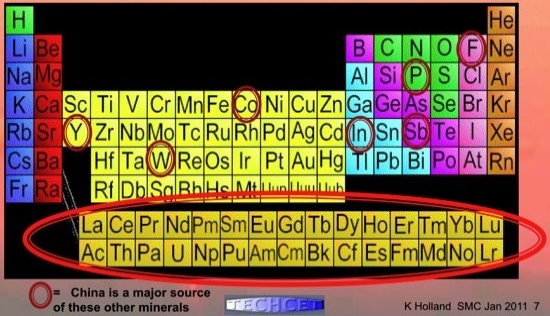
The materials analyst session led off with Karey Holland of Techcet Group. (‘Techcet’ is a palindrome of ‘tech’ forward and backward, but you all knew that by now, didn’t you?) The silica market is going gangbusters, and not because of CMP — it’s the increasing use of western-style toothpaste in China. There is no relief in sight for anxieties surrounding rare earth & other element supply constraints from China. Beyond rare earths, China’s mineral export restrictions are impacting WF6, phosphoric acid and HF supplies. Ta had been supplied mostly from the Congo, which is now prohibited as a ‘conflict mineral;’ the other main source in Australia had been shut down for not being economical. Funding lithography R&D for exposure tools and resist materials continues to challenge suppliers, particularly in light of still decreasing volumes of resist per wafer. There are still >9 players in resist and ancillaries; >20 players in CMP slurry, many continuing to gain market share, IP lawsuits notwithstanding.
 Click to Enlarge
Rare earth elements are not so rare…

Continuing the materials and markets theme, Michael Corbett at Linx Consulting took a closer look at emerging materials in advanced devices. Did the ‘Decade of Materials’ (as declared by earlier SMC meetings) really begin in 2000? Based on SMC agendas, a decade ago, no one was talking about 450mm, PV, LEDs and 3D ICs. The materials market doubled from $20.3B in 2000 to $38.1B in 2010 (a 6.5% CAGR), with some of the largest growth in plastic substrates, bonding wires, CMP consumables and silicon wafers themselves.

Click to Enlarge

Mike’s conclusion was Yes, it was, as evidenced by the entry of large chemical companies BASF, Dow and DuPont into the semiconductor side of the materials biz; and the successful introduction of high-k metal gates and litho alternatives. Low-k dielectrics was scored as a mixed bag, with successful implementation that is below expectations. The bifurcation of device and process types below 90nm continues to drive materials development demand.

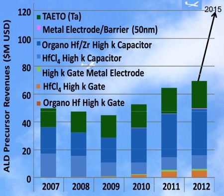
The ALD/CVD precursor market is expected to triple over the next five years. Adjacent markets have matured from being new target markets for suppliers to being competitors that can impact materials availability for semiconductors. These include PV, displays, and compound semiconductors; LEDs have not yet appeared on this radar.
Click to Enlarge

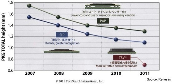
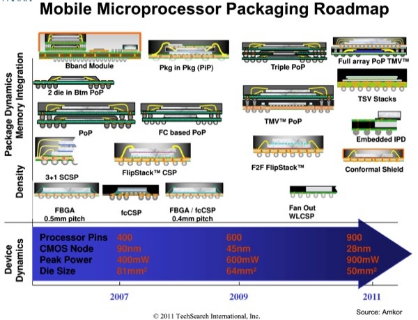
Defending the honor and value of semiconductor packaging materials, E. Jan Vardaman of TechSearch International launched a rapid-fire assault on a mountain of data — remember that the variety of packages is several orders of magnitude greater than the number of types of semiconductor devices. A trend from flip chip to wire bond began at 65nm. At the same time, by 2014 flip chip, WLP and Au bumps will account for 16% of IC shipments. Over the next 5 years, flip chip is projected to grow at 15%, with a shift to Cu pillar; WLP at 12.5%, with a shift from BCB to PI or PBO, and increasing use of fan-out. Nearly all smart phones use 3D package-on-package, giving this design a 27% CAGR. TSV implementation continues to be pushed out due to reliability data and supply chain infrastructure that still needs to be established for each device type. Jan put it succinctly: "TSV needs to move from PowerPoint to real engineering work." LEDs are going to drive a large set of packaging materials, many derived from existing supply chains, many not.
Click to Enlarge
Mobile microprocessor packaging roadmap.

Click to Enlarge
Trend of stack SIP package height.

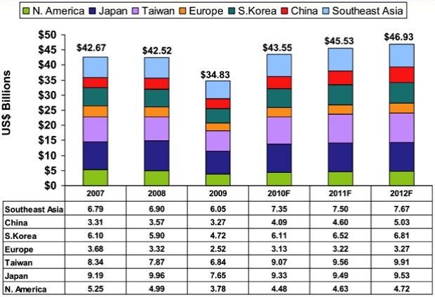
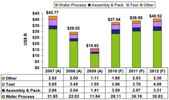
Dan Tracy of SEMI took a look at the industry and investment outlook. His overall materials revenue data for 2010 is $43.8B, while equipment is $37.5B. [Remember your basic calculus: equipment revenue tracks the first derivative of new capacity, and material revenue tracks the integral of the installed base.] Wafer shipments from Asia-Pacific are now >50% of total silicon area. Japan is still #1 in overall chip fab capacity, but they are #3 in 300mm capacity. Taiwan has passed the US to the #2 spot overall, followed by Korea, Europe, SE Asia and China. In packaging capacity, SE Asia and Taiwan lead, with China expected to pass Japan for #3 this year; Korea follows, with Europe & Americas trailing. Growth forecasts for 2011 are 6% for Si, 5%-6% for fab materials, and 3.5% for packaging.
Click to Enlarge
2010 year-end equipment forecast by segment. Totals may not add due to rounding.
(Source: SEMI Year-end 2010 Semiconductor Consensus Forecast, Dec. 2010)
Click to Enlarge
Materials forecast by market region. Totals may not add due to rounding. (Source: SEMI, Jan. 2011)

A panel of these four speakers was moderated by Lita Shon-Roy of Techcet Group. Gold price escalation is driving an increased fervor for alternatives to wire bond. CMP steps will continue to be added as NAND overtakes DRAM. There is a collective of 1μm production volume that is poised to migrate to 0.25μm 200mm, which may sustain the demand for older material sets such as Al & Ti targets and W slurry. New capacity is still being added for 248nm resist. Supplementing Chinese rare earths with sea floor nodules is a possibility, but it’s more likely that as prices rise, new conventional mines will open or re-open outside of China. Supplier consolidation in front-end materials is slowing as the number of opportunities declines. Opportunities still exist in ALD precursors. Even though there are still ~20 slurry suppliers, they are now parts of larger companies. Packaging is still very active and the supplier base will continue to shrink. The trend to Cu wire bonds will take a huge chunk out of packaging revenues as Au is displaced. HKMG will collectively drive modest volumes of materials usage, but they are critical and will be extremely sensitive too supply constraints. The cost of Ru is likely to moderate its implementation and supply sensitivity. IP protection globally will more likely be improved by cultivating the appropriate company culture than by legal enforcement efforts. More Than Moore brings several new materials markets with it, but R&D funding strategies need to keep up with increasing costs and decreasing volumes per wafer.

The final speaker of SMC 2011 was Matt Gertken, Asia Pacific analyst for Stratfor (short for Strategic Forecasting), with a geopolitical perspective on what is happening in the world that affects our markets:

  • US demographics are in relatively good shape compared to China, Japan, and Germany with respect to sustained GDP growth, due in large part to immigration. The US may need to maintain its presence in Iraq to mitigate movements by Iran, which is the region’s dominant conventional military power.
  • The European debt crisis is exacerbated by southern European economies that traditionally rely on lower-tech and less sustainable industries.
  • China’s assertive foreign policy extends to accelerating resource acquisition, territorial disputes, and a huge investment in infrastructure in border areas. The Chinese restriction on rare earths closely followed a clash with the Japanese Coast Guard. The US has fully re-engaged in the AP region with new more balanced trade agreements. The Korean peninsula is destabilized by the impending succession of power in North Korea in 2012.
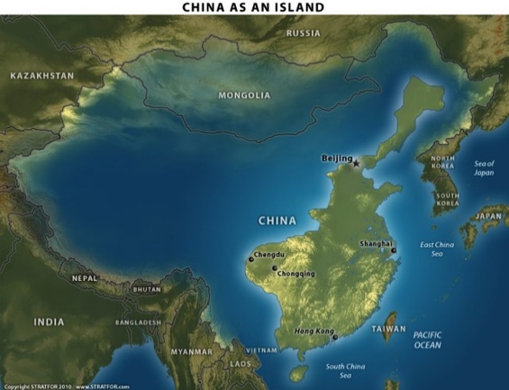
  • One important angle to understanding dynamics within China: the vast majority of its population is limited to a number of regions, with the remainder of the territory very sparsely populated as a buffer area.
  • Rising costs in China is leading to the collapse of several export businesses. China exports are already at the 10% global level, which is about where Japan topped out at its peak. Consumption is still <40% in China; US consumption at 70% is larger than Russia, China, Japan and Brazil combined. Fearing that growth would slow, China has unleashed a bank loan spree, increasing the level of unserviceable debt. This is the scenario that Japan experienced in the 1990s, with disastrous consequences.

  • China is facing a generational change of leadership in 2012, both government and military. The current leadership has lacked the stature to anoint their own successors, which helped maintain stability in the past few transitions.
  • China is holding more than $850B in US long-term treasury debt. However, the Chinese share of the US trade deficit is stable to shrinking, indicating some movement to improve the balance. Banks in China avoided the sub-prime collapse largely because home buying is highly capitalized with 40% down payments typical. 
Click to Enlarge

The next ISS & SMC meetings are scheduled for the week of January 15-20, 2012 returning to the Ritz-Carlton, Half Moon Bay, CA.


Michael A. Fury, Ph.D, is senior technology analyst at Techcet Group, LLC, P.O. Box 29, Del Mar, CA 92014; e-mail [email protected].