Category Archives: MEMS

October 14, 2009 – SVTC’s efforts to offer more leading-edge MEMS technology for its customers now finds it more formally aligned in a new partnership with the world’s biggest semiconductor foundry.

Under a new alliance, SVTC and TSMC will work with developers to support new products from concept to volume production and commercialization, centering on technologies for applications in "emerging markets" — e.g., MEMS, biochips, and other devices with new materials and structures — "whose ideas or products are based on silicon technologies, but may not necessarily scale with Moore’s Law," noted Joseph Bronson, SVTC CEO, in a statement. "There are a number of promising applications that could inspire entire new industries, but many lack a clear path to commercialization and high-volume manufacturing," and the new ties to TSMC will help "the world’s most promising innovators to develop new products and to bring the best of these new devices into volume production."

Development and early commercialization work on "conceptual or undeveloped" products will be done at SVTC; as demand increases, the processes will be transferred over to TSMC for volume manufacturing, with both firms co-marketing unspecified services.

SVTC and TSMC have been partners going back to a "technology incubation program" announced shortly after SVTC was spun out of Cypress Semiconductor in 2007, fulfilling one of SVTC’s first goals of developing closer ties with foundries as a type of referral service. SVTC now offers a "Fast-Transfer" process to help improve yields for products transferred to TSMC.

In 2008 SVTC started offering 200mm MEMS development, in a bid to leverage synergies with integrating MEMS and logic technology (i.e. base CMOS). There’s a learning curve in such a migration with many tool advances and changed processes to be accounted for, as Scott Marquardt, VP of sales, marketing, and strategic business development, told Small Times: "You can’t just take what you’re doing in 6-inch and send a diagram off to TSMC and say, ‘Please make me 10 million of these.’"

October 9, 2009 – IMEC’s annual IMEC’s annual Technology Forum this week featured three announcements targeting medical devices: a low-power MEMS actuator for in-vivo biomedical applications, a microfluidics device for faster cancer detection and therapy, and a new wireless EEG system for ambulatory monitoring.

"Inchworm" actuator for in-vivo biomed

An ultralow-power, watertight actuator newly developed by IMEC targets applications requiring long autonomy with small batteries, and is "especially suited" for in-vivo biomedical applications such as brain implants, the R&D consortium says.

The new silicon-on-insulator (SOI)-fabricated device is an "electrostatic inchworm actuator" that converts energy into micromovements — by moving in concert, four arms that selectively latch/unlatch and two for driving can achieve a bidirectional step-like movement. The device has a range of ±50μm and can generate sufficient force (±195μN) to position, for example, in-vivo brain electrodes, with 3× lower operating voltage (11V) than current actuators, and it also consumes just <100nW of power. The device has been integrated with a microneedle encapsulated in a flip-chip package with a glass cap and hydrophobic surface treatment (i.e. it’s watertight).


Click to Enlarge
Click to Enlarge
Figure 1. Schematic (top) and micrograph (bottom) of IMEC’s inchworm actuator, with six pull-in actuators (four for latching and two for driving). By proper latching, unlatching, and driving the shuttle, the actuator can drive a bidirectional step-like movement. (Source: IMEC)

Micro-actuators are already used in medical applications requiring microscopic-scale control of biological objects or environments — e.g. for microsurgery tools, pumps, and needles. One application is to integrate the actuators with microprobes for brain applications, for accurately controlling the position of microneedles, so as to reach and get near the correct groups of neurons for a specific disorder to obtain the best signal/noise ratio. These would be true "implants" in the sense of the word; today’s "implants" using actuators for brain research are actually placed outside the body.

Click to Enlarge Click to Enlarge

Figure 2. Schematic (left) and actual photo (right) of the actuator, encapsulated with a micro-needle in a watertight package. (Source: IMEC)


Lab-on-chip targets breast cancer

Under the European Union’s MASCOT ("Multiple-access space-time coding testbed") project which pursues "novel techniques" for multiple user/input/output wireless systems, IMEC and partners have put together a modular platform with autonomous modules which can be used for different medical applications — in this case, detection and therapy evaluation of breast cancer.

This particular device — the first to include many complex sample preparation steps and multiplexed detection, according to IMEC — includes one module for mixing blood samples with magnetic beads that bind to tumor cells, and another module to isolate and count those cells using dielectrophoresis and magnetic sensing. In the third "amplification" module the tumor cells are destroyed and the genetic material extracted using multiplex ligation dependent probe amplification. Specific assays amplify ~20 markers associated with breast carcinoma cells, which are detected using an array of electrochemical sensors.

Having a multifunction lab-on-a-chip device would solve timeliness and cost issues associated with cancer detection, IMEC explains. In the case of breast cancer, only 2-3 tumor cells are found in 5ml of blood; many sample preprocessing steps in different medical instruments are required to make full analysis. A lab-on-a-chip system incorporating the above-described functions would vastly simplify this process, which could be performed in a doctor’s office or near a patient’s bedside.

The system has been validated on "spiked blood samples" and modules are ready for "further hetero-integration into a single lab-on-chip," IMEC notes. Next is to clinically validate it in a breast cancer therapy study in Oslo.

Wireless EEG

IMEC and research affiliate Holst Center have developed a miniaturized wireless EEG system for remote monitoring of patients in their daily environment; the result is seen to be more natural readings and more comfortable patients.

The system incorporates an eight-channel ultralow-power analog readout ASIC, with other electronics including radio and controller integrated onto a 47×27mm printed circuit board, packaged in a "small box" with status LEDs, a switch button, and interfaces for din32 cables. The whole thing requires only 1.8mA of power, meaning about three days of operation on one 160mAh lithium ion battery.

The system can connect to individual electrodes, recording high-quality signals via gel electrodes (R&D on dry electrodes is still ongoing), standard EEG monitoring hats, or other proprietary EEG headsets. Data is wirelessly transmitted in real-time to a receiver up to 10m away. IMEC also has developed algorithms to interpret the brain signals, "linking the brain activity to the degree of relaxation," the group said in a statement.

The new wireless EEG is part of an art expo, dubbed "Staalhemel" ("Steel sky"), at the center STK in Leuven, Belgium, in which visitors wearing a headset with IMEC’s EEG system walk past 80 steel plates suspended above; the brainwaves activate tiny hammers to tap rhythmic patterns on the plates.

October 6, 2009 – Among a spate of presentations at this week’s annual IMEC Technology Forum in Belgium, the European R&D consortium trotted out a new program for foundries and fabless companies, an "incubation" pact with TSMC, and developments in multithreading and radio chips. Other news out of ITF involved solar and medical device technologies.

Bridging the IC gap with INSITE

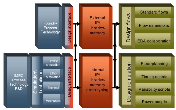
A new addition to IMEC’s industrial affiliation program, the Integrated Solutions for Technology Exploration (INSITE) program is a framework within which fabless and fab-lite companies, foundries, and EDA firms can work on early product developments that are "one to three generations ahead of IC manufacturing," to design either in process technologies from IMEC’s core CMOS research program or "more imminent foundry-level technologies." The program’s modular framework incorporates a design interface, circuit level IP generation, and pathfinding, with fabrication/measurement of 200mm-300mm-based test circuits in IMEC’s facilities.

Click to Enlarge
IMEC’s INSITE framework of extensible, flexible modules. (Source: IMEC)

The goal, according to IMEC, is to stem two trends that are creating a "growing knowledge gap" between digital CMOS producers and users. The first is a move to separated foundries and fabless design houses and away from integrated design/manufacturing. Each side may have different needs and questions, but "the solutions to their questions require collaboration and dialog between all parties" notes Phillip Christie, principal researcher at IMEC, in a statement.The second trend is an evolution toward more application -specific technology offerings where specifications such as speed, power, area, and cost can’t be achieved with the same technology.

Incubation with TSMC

Another thrust into leading-edge chip development is a new "Innovation Incubation Alliance" forged with TSMC, to combine IMEC’s design/R&D and TSMC’s high-volume manufacturing. The partnership provides access to technologies from IMEC’s CMORE initiative — e.g., various flavors of IMEC’s "Moore than Moore" offerings, ranging from mixed-signal to 3D-technologies, MEMS processes, Si photonics, and BiCMOS/HV — through product concept validation (QC, design & test, packaging, reliability), low-volume manufacturing at IMEC, and transferral to high-volume manufacturing at TSMC.

Click to Enlarge
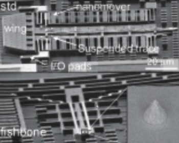
XSEM overview of IMEC’s standard and fishbone cantilever designs with suspended Pt trace and sharp tips. (Source: IMEC)

"We are convinced that by joining our strengths, the IMEC-TSMC Innovation Incubation Alliance will offer customers an industry wide platform to rapidly bring innovative products to market," said Maria Marced, president of TSMC Europe, in a statement. "By linking IMEC’s R&D skills with TSMC’s manufacturing skills during the product development phase, the transition of More-than-Moore technologies to high volume manufacturing will accelerate," added Luc Van den hove, IMEC’s President and CEO.

Multithreaded processor architecture

IMEC also unveiled the 40nm-based, 2nd generation of its "architecture for dynamically reconfigurable embedded systems" (ADRES), with double the performance and energy efficiency (600Mbps 802.11.n on two cores, 220mW power use) than its predecessor and added support for multithreading. The technology, ready for licensing to chip manufacturers, is billed as "a building block for future 4G devices" such as mobile terminals including software-defined radios, and is "a stepping stone" to research into building a baseband processor that can support full 4G requirements: gigabit/sec wireless connectivity, runtime resource management, and support for 4×4 MIMO and latest WiFi/LTE standards.

Liesbet Van der Perre, director of IMEC’s wireless communications program, noted a proof-of-concept 40MHz WLAN MIMO reciever has been mapped, and that next year ADRES will be extended with wide SIMD (vector instructions) to better energy efficiency another 30%.

Custom-designed radio ICs

Meanwhile, IMEC and spinoff AnSem are collaborating to offer services for custom designs of radio ICs, for companies who want to outsource design and development of what they’ve done with IMEC’s research into communication ICs. Offerings include: IMEC’s first-generation flexible radios, reconfigurable transceivers tunable for any cellular, WLAN, WPAN, broadcast, and positioning standards.

"Both IMEC and AnSem bring their complementary expertise to the table," noted Stefan Gogaert, CEO of AnSem, in a statement. "IMEC has a strong background in technology innovation and exploration, while AnSem is the expert in design services for analog and mixed-signal ICs. The combination is a unique customization and productization offering."

The service "lowers the threshold for companies to launch innovative communication products, and reduces the risk, effort, and time to market," added IMEC’s Van der Perre.

September 29, 2009 – Researchers at the National Institute of Standards and Technology (NIST) have come up with a way to use microfluidics to generate microdroplets containing single molecules, which using "optical tweezers" could be merged into multiple droplets to get their contents to react, ultimately informing about the structure and function of organic materials such as proteins, enzymes, and DNA.

Click to Enlarge
Water flows through a microfluidic channel (35μm wide) into a narrow constriction, where it breaks up into droplets. Varying the width of the constriction changes the size of the drops and lacing the water with desired molecules of just the right concentration causes the resulting droplets to pick up single molecules. (Source: NIST)

The work by NIST physicists Carlos López-Mariscal and Kristian Helmerson involved creating a microfluidic device with a narrow channel through which water, squeezed into a narrow stream by oils, can flow; its abrupt pressure drop (and an added "dash of detergent") breaks the surface tension, creating small droplets of uniform size (1μm, or 0.5 attoliter volume), adjustable by tweaking the constriction’s width. The water droplets are then "laced" with molecules of precise concentration so that each picks up "on average" only one molecule of interest, 99% of the time. They can then be moved by laser beam into each other to coalesce, with reactions observed through "optical methods."

Initial work involved mixing fluorescent molecules emitting different colors; future work could involve "more interesting chemical reactions, such as those between an infectious agent and an antibody, or a chromosome and a drug." The laser beam also can be shaped to capture arrays of the molecule-carrying water droplets, opening up new possibilities for single-molecule spectroscopy."

The work was published in August 2009 by the SPIE (Proc. SPIE, Vol. 7400, 740026 [2009]).

NIST also has a video showing the use of microfluidics to produce the highly-uniform water droplets — click here.

by Martin G. Selbrede, Uni-Pixel Displays Inc.

Alternatives to silicon-based MEMS displays have the potential to reach new levels of optical performance. These alternatives impose unique demands on thin polymer membranes with respect to electrical, mechanical, and optical performance. New membranes are being developed that meet the requirements for use in field sequential color displays based on frustration of total internal reflection.

September 25, 2009 – Industry interest in field sequential color (FSC) displays has, in part, been driven by the reduction in complexity they make possible. Instead of three separately-driven sub-pixels (one for each primary color) comprising a single conventional pixel (a tricellular pixel), FSC displays generate all colors from a single unicellular pixel by exploiting the temporal resolving properties of the human eye. As a consequence, while FSC displays enjoy reduced complexity in the number of features, their pixel response times must be significantly faster than non-FSC displays. This is especially true if gray scale is achieved digitally using pulse width modulation (PWM), as would likely be true in MEMS-based FSC display systems.

 Click to Enlarge
Figure 1. Conceptualization of the layers comprising an AM-LCD system

The incumbent flat-panel technology, liquid crystal displays (LCD), provides a benchmark for conventional tricellular performance in transmissive display systems. The advantages of a MEMS-based FSC display, relative to a modern LCD system, are not limited to reduced complexity of design. Optical performance, particularly with regard to power efficiency, can be substantially greater for FSC-based MEMS displays. This is a natural result of the large sequence of layers at the heart of LCD systems, most of which serve to attenuate light passing through them. Polarizers, color filters, pixel apertures, all conspire to reduce the final output of an LCD system to a small fraction of the initial light entering the panel from the backlight subsystem (Figure 1).

MEMS-based FSC systems can do without most of the light-attenuating layers that are required for LCD operation, and without these sources of energy attenuation, the power efficiency of MEMS-based FSC displays can exceed that of LCD technology by nearly an order of magnitude (Figure 2). For FSC displays, where the principle of pixel operation is the frustration of total internal reflection [1] (FTIR), most of the source light (theoretically, >60%) makes it through the display layers to the viewer, as compared to 3-8% for most LCD systems. The efficiency of light output for FSC FTIR displays is a design tradeoff. Maximum efficiency is achieved at the expense of display uniformity thus; the overall system design strives to achieve the maximum power efficiency possible without harming the luminous uniformity of the output. Our research has shown that the optimal balance is at 61% efficiency.

The demands upon the polymer membrane at the heart of a polymer MEMS-based display that uses an FSC FTIR approach to light transmission are significant. Optimizing the electrical, mechanical and optical properties of such a membrane is the key to successful implementation of these novel approaches to display fabrication.

 Click to Enlarge
Figure 2. Conceptualization of the difference in light attenuation between FSC FTIR display (left) and LCD technology (right).

Polymer membranes

Uni-Pixel Displays is developing an FSC FTIR display system, called a "time-multiplexed optical shutter" (TMOS), based on a polymer membrane capable of MEMS actuation. The optimization of that technology has led to the creation of Opcuity films, an innovative series of polymer membranes.

The principle of operation of a TMOS display involves suspending a sheet of the new polymer membrane film about one micron above a slab waveguide, using low-optical-impact standoffs at the perimeter of each pixel. In the quiescent, inactive state, the new film remains suspended above the waveguide such that light traveling inside the waveguide, according to the principle of total internal reflection (TIR), is unable to be transferred into the film and redirected out to the observer. The one micron gap places the new polymer membrane film sufficiently far outside the evanescent field of the waveguide [2] to prevent any appreciable light leakage in the pixel off-state.

During pixel actuation, the membrane is electro-statically pulled into contact, or near-contact, with the waveguide. TIR is thereby frustrated and the light that was otherwise contained within the waveguide will pass into the film and be directed out to the viewer. When the electric field is discharged, the film returns to its former position a micron away from the waveguide, causing light transmission to cease.

The three primary colors, red, green and blue, are injected into the waveguide from one (or more) of its edges. Rapid sequential cycling of the primary lights provides the background energy to be modulated by the individual pixels using the principle of PWM. Rapid on-and-off actuation of the film at each pixel makes it possible to achieve a wide color gamut in an FSC PWM display system.

The new polymer membrane films must meet three key physical criteria (mechanical, electrical, and optical) to be suitable for deployment within the targeted polymer-MEMS display system. Balancing these criteria in one planar polymeric structure is central to the new film’s architecture.

Mechanical criteria for polymer MEMS systems. The mechanical criteria for the polymer MEMS systems are pertinent to rapid actuation over long display lives. Due to the aspect ratio of the pixel (pixel area divided by the one-micron gap between film and waveguide), the actual strains imposed on the elastomer comprising the polymer-based Opcuity film are well under the polymer’s elastic limit, providing a large safe operating area to prevent degradation of the spring constant.

The polymer film, however, must exhibit high mechanical robustness for other reasons. The mechanical stiffness of the membrane has a bearing on the operational voltage of the pixel, and is a power function of the thickness of the film. Some polymer membrane substrates are as thin as three microns and yet must support an array of micro-optical structures on the waveguide-facing surface. Moreover, the mechanical potential energy stored inside membranes during pixel actuation is necessary for returning the pixel to its quiescent state (passive release of the pixel). Passive release allows for simpler architectures; the alternative is active release, whereby the polymer membrane is electrostatically pulled off the waveguide. Currently, all Opcuity films have met the requirements for passive release of actuated pixels.

The final mechanical requirement is that stiction at the point of contact between the polymer membrane and the waveguide be kept to a minimum. The higher the stiction, the greater the energy needed for passive release, which entails higher operating voltages for the display.

Electrical criteria for polymer MEMS systems. Because the power draw on an electrostatically driven pixel rises exponentially as a function of the gap between the conductors, the polymer membrane must be configured to provide the smallest possible inter-conductor spacing. A TMOS pixel is a variable capacitor, having one capacitance in its quiescent state and a somewhat larger capacitance in its activated state. One plate of the capacitor is a transparent conductor applied directly to the waveguide surface, while the other plate is borne by the membrane.

Optical criteria for polymer MEMS systems. The optical coupling efficiency of the membrane film is a function of several different parameters. It is actually undesirable for the membrane film to have an excessively high coupling efficiency. However, due to the inherent recycling of light that arises within the slab waveguide — owing to the non-insertion edges being suitably mirrored to keep light inside the waveguide until emitted by a pixel or absorbed at the system sink — a film exhibiting moderate optical coupling efficiency still delivers a global power efficiency of 61% or better.

 Click to Enlarge
Figure 3. Photomicrograph showing the micro-optical structures protruding from the interstitial conductor. The flat tips of the frustums have no conductive material on them.

The surface of the membrane film that faces the waveguide has an array of micro-optical structures integrated into the polymer. These structures are designed to achieve several goals: 1) extract light efficiently from the waveguide; 2) shape the extracted light into an ergonomically useful output distribution; 3) enable efficient final emission to the viewer without undue scattering or absorption; 4) limit the amount of light being coupled based on the effective surface area in contact with the waveguide during pixel actuation; and 5) provide a standoff that keeps the conductor on the membrane film from contacting the conductor deployed on the waveguide.

This last function arises because the conductor is situated between the micro-optical structures (Figure 3). The interstitial conductor between the micro-optical structures (which are conical frustums in the particular sample of membrane film shown in Fig. 3) does not extend to the flat tip of the frustum. When the frustum tips contact the waveguide during pixel actuation, there remains a gap between the conductor on the waveguide and the interstitial conductor situated between the frustums. This feature of the membrane film provides the lowest possible operating voltages for pixel actuation.

The membrane film has applications beyond FSC displays. Films have been designed that have resistance to retaining any fingerprints. Fingerprint-resistant films represent an important additional market for the membrane film.

Membrane films: key to FSC FTIR display systems

Designing optical thin films for deployment in MEMS systems, where the film is expected to be in rapid repeated motion for billions of cycles, is an undertaking that involves the multidisciplinary application of physical and engineering principles. Films that can meet the requirements for these applications enable the furthering of new and novel next-generation displays, such as Uni-Pixel’s TMOS technology, that are able to deliver optical performance at reduced costs. Uni-Pixel’s polymer membrane films are being developed to meet the requirements for next-generation display systems and for production using roll-to-roll fabrication techniques to further reduce manufacturing costs

In principle, active matrix fabrication facilities can be readily converted from LCD manufacturing to TMOS manufacturing, since TFT mother glass serves as a suitable waveguide for many display applications. Laminating the polymer membrane film onto the TFT layer provides for promising new manufacturing opportunities for older fabs.

Conclusion

Uni-Pixel’s FSC FTIR display technology currently exists as a hybrid system that utilizes flexible micro structured film in combination with a TFT rigid glass backplane. We envision that in the future the entire display can become a flexible structure. Any technological barrier to producing an all flexible FSC TMOS display will disappear as printed electronics matures and low-cost reliable TFTs on thin flexible films become available.

Acknowledgments

Opcuity is a trademark of Uni-Pixel Displays Inc.

Biography

Martin G. Selbrede is chief scientist at Uni-Pixel Displays, Inc., 8708 Technology Forest Pl., Ste. 100, The Woodlands, TX USA; ph.: (281) 825-4500; email [email protected]; www.unipixel.com.


References

[1]. S. Zhu, A. W. Yu, D. Hawley, R. Roy, "Frustrated Total Internal Reflection: A Demonstration and Review," Am. J. Phys. 54 (7), pp. 601-607, July 1986.
[2]. F. de Fornel, "Evanescent Waves: From Newtonian Optics to Atomic Optics," first edition, Springer-Verlag, New York, 2001, pp. 18-28. 


September 21, 2009 – MIT researchers say carbon nanotubes formed into tiny springs can store as much energy, pound-for-pound, as lithium-ion batteries, and offer better durability and reliability.

Based on two papers — a theoretical analysis in the June issue of the journal Nanotechnology, and a laboratory demonstration in the September issue of the Journal of Micromechanics and Microengineering — indicate that carbon nanotube springs could store more than 1000× more energy for their weight than steel springs, and comparable to state-of-the-art lithium ion batteries.

Two key differences indicate springs’ advantage over traditional batteries: they can deliver store energy either in a rapid, intense burst, or slowly and steadily; and their stored energy doesn’t leak out over time.

Applications for such CNT springs could be emergency backup power supplies that go years untouched until needed without testing or replacement; portable devices in place of gasoline engines; or sensors in harsh environments where conditions like temperature or pressure extremes (e.g., boreholes for oil wells) would affect performance of traditional battery technology. First uses are likely in larger systems, not MEMS devices, since storage and release of energy in such springs is of a mechanical nature and not necessary to convert into electricity, notes MIT prof. and co-author Carol Livermore, in a statement.

Next steps in the work are to test actual performance over time, to confirm the CNT springs can charge and recharge without performance loss, and more research and engineering to determine how close devices using them could come to theoretically possible high energy density. Current CNT growth methods need to be improved to make more desirable highly concentrated CNT bundles with longer, thicker fibers, instead of the CNT fibers joined in parallel made in initial lab tests.

September 11, 2009:  Researchers at the National Institute of Standards and Technology (NIST) say they have a new method to improve temperature calibration for microfluidic systems.

Typically, reactions in microfluidic systems require some form of heating, and monitoring temperature changes in fluid volumes ranging from microliters to subnanoliters — DNA analysis relies on precise temperature cycling, for example. An alternative to thermometers and temperature probes, which are generally not effective at these dimensions, are noninvasive temperature-sensitive fluorescent dyes (e.g., rhodamine B), whose intensity is inversely proportional to temperature (i.e., as temperatures go up, their intensity goes down). The technique, though, requires basing all reading on the fluorescence at a single reference temperature. Others (NIST researchers, in 2001) have devised "calibration curves" to relate temperature to rhodamine B fluorescent intensity, using a reference temperature of about 23°C, but those are only good for that one temperature.

The new work, described in a paper for Analytical Chemistry, shows that changing the reference point in a microfluidics system (e.g., higher temperatures when first heated) introduces significant errors with such dye intensity calculations using current method — up to an 11°C range of error (-3°C to 8°C) for calibration equations derived at ~23°C, using a simple linear correction for a 40°C reference temperature, according to lead researcher Jayna J. Shah.

To address this, the team devised mathematical models to correct for the shift during reference temperature changes; with this they created generalized calibration equations that can be applied to any reference temperature. Among the applications is amplifying microfluidic DNA (producing numerous copies) by the polymerase chain reaction (PCR), which requires cycling a microfluidic device to be cycled through temperatures at three different zones, starting around 65°C — a dye intensity-to-temperature ration would have to be based on that temperature, not the aforementioned 23°C, Shah notes.

September 8, 2009: Panasonic Electric Works has developed a sensor system that recognizes facial features in all lighting: dark, overly bright, and even behind glass, reports the Nikkei Business Daily.

The system, for use in a charge-coupled device (CCD) camera, combines an LED modulated light source for near-infrared light with image-processing circuitry, so that only near-infrared light reflected from the subject is processed; the resulting sharp image  (QVGA-quality monochrome) is captured for face-recognition processing even in bright light that would wash out features, or as a car windshield reflects surrounding scenery, the paper notes. LED modulated light also is unaffected by sunlight or other sources, so it can work in the dark.

The sensor system allows shutter speeds up to 0.002 seconds, capable of identifying passengers in cars traveling up to 50kph; subjects can be up to 2-3m away (or up to ~10m by adding more LEDs).

Commercialization for the sensor system is planned for spring 2010; initial applications include security/crime prevention, such as cameras in structures like buildings and parking garages, and biometric identification. ATMs also could use the system to identify users by hand vein patterns, since conventional biometric readers encounter interfere by bright light in outdoor settings.

by Debra Vogler, senior technical editor

A new Microelectronics Innovation Center is being formed at the Université de Sherbrooke in Bromont, Québec, to focus on 200mm-based microelectromechanical systems (MEMS) and 3D wafer-level packaging (WLP), and "advanced technologies associated with the assembly and packaging of silicon chips." Initial investments come from the governments of Québec ($94.95M) and Canada ($82.95M), and another $40.6M from center cofounders DALSA Semiconductor, IBM Canada, and the U. of Sherbrooke along with unidentified semiconductor equipment suppliers. Participatory interest is said to have been expressed by other universities, research centers, and industrial partners both in Canada and globally.

The prime purpose of the innovation center is to leverage the best from the Canadian and international research community to address industry’s most challenging problems, with the end goals of technology transfer as well as development of spinoffs. It also will be the centerpiece of a planned "true microelectronics cluster in Québec," hoped to extend from activities centered around Albany, NY. An estimated 250 researchers will be involved, and >3000 jobs will be created.

DALSA will assist in the design of the center and take a lead role in the specification, installation, and ongoing operational responsibility for the MEMS- and WLP-related equipment, which the company says will be among the most advanced in the world for 200mm MEMS and 3D WLP processing.

Claude Jean, VP and GM of DALSA Semiconductor, told SST that the center enables pre-competitive research — not in fundamental R&D, "but rather take already existing results and do the last step needed to bring the technology to volume production."

The new center not only benefits from DALSA’s founding participation and support, but the company gains an advantage in participating in the center as well. For example, the company cannot bring gold into its MEMS production foundry because of CCD manufacturing going on in the facility; isolation capabilities being built into its production house will not be complete for about a year. The new research center does have isolation capabilities, so work can be done using gold without delay. — D.V.

September 2, 2009: A new Microelectronics Innovation Center is being formed at the Université de Sherbrooke in Bromont, Québec, to focus on 200mm microelectromechanical systems (MEMS) and 3D wafer-level packaging (WLP), and “advanced technologies associated with the assembly and packaging of silicon chips.”

Initial investments come from the governments of Québec ($94.95M) and Canada ($82.95M), and another $40.6M from center cofounders DALSA, IBM Canada, and the U. of Sherbrooke along with unidentified semiconductor equipment suppliers. Participatory interest also has been expressed by other universities, research centers, and industrial partners both in Canada and globally, they note.

The group’s stated “prime purpose” is to “leverage the best from the Canadian and international research community to address industry’s most challenging problems,” with end goals of both technology transfer and spinoffs. It also will be the centerpiece of a planned “true microelectronics cluster in Québec” hoped to extend from activities centered around Albany, NY. An estimated 250 researchers will be involved, and >3000 jobs will be created.

“The project marks the birth of a value chain that could eventually match the Québec economy’s flagship innovation sectors — life sciences, aerospace, and computer technologies,” said Clément Gignac., Minister of Economic Development, Innovation and Export Trade, in a statement.