Category Archives: Energy Storage

July 21, 2011 – Marketwire — SolRayo, Enable IPC Corporation (PINKSHEETS:EIPC) subsidiary,  developed an inexpensive and simple nano-based technology to improve lithium batteries, using its Small Business Technology Transfer (STTR) grant from the National Science Foundation (NSF) SBIR/STTR Program. The $150k grant, awarded in 2010, enabled SolRayo to create a nanoparticle-based technology to address performance degradation of certain lithium batteries, particularly in high-temperature applications.

The nanoparticle coating approach is "simple and inexpensive," according to SolRayo CEO Dr. Mark Daugherty, benefiting lithium battery cycle life (number of charges and discharges) by a factor of three. The nanoparticle coating inhibits the degradation of battery cathode materials, especially at higher operating temperatures, explained Kevin Leonard, SolRayo CTO.

The NSF approved SolRayo’s final report, clearing the company to submit a Phase II proposal for an additional $500,000 in funding over two years beginning in early 2012. Phase II objective will be commercialization of the technology in military, remote power and transportation applications, said Daugherty, fulfilling the STTR program goal of transfering technologies from lab to marketplace.

Battery makers and battery materials suppliers have checked out the nano coating, and SolRayo has seen "some strong interest in the technology," said David Walker, Enable IPC CEO and SolRayo COO.

STTR is a US government-funded, highly competitive small business program that expands funding opportunities in the federal innovation research and development arena.

Enable IPC provides efficient, streamlined strategies for turning technologies into products and bringing them to market. Learn more at http://www.enableipc.com

Also read: Nanotechnology improves Li-ion battery capacity

Visit our Energy Storage Trends blog.

by Steve Leone, RenewableEnergyWorld.com

July 12, 2011 For an industry with as much momentum as solar, it’s still a healthy reminder that only 1% of America’s electricity supply comes from the sun.

Right now, solar is mostly a peak generation provider. For it to get where it needs to go, it needs to move into baseload territory — namely, the space dominated by fossil fuels.

To achieve that end, the solar industry and other renewables have to lay the groundwork for a new energy economy focused on smart solutions to some current limitations. That was the view presented by Andrew Skumanich, CEO of Solar Vision, during his presentation Monday morning at the opening day of the Intersolar conference in San Francisco, which runs through Thursday.

Here’s what Skumanich laid out as some of the key considerations if the US and other emerging markets are really to achieve their solar potential:

Appreciate the challenge. Utilities have always had to manage intermittency on the demand side, but now they have to manage it on the supply side as well. This creates an extraordinarily complex configuration. Right now, utilities are concerned about dependability at about 20 to 30 percent integration.

We must deploy available solutions. These include smart meters with time-of-day pricing, co-generation with PV-natural gas partnerships and forecasting that happens by the week, day and hour.

Energy storage goes way beyond batteries. It’s still costly and still at the research and development level. This remains true even with Concentrated Solar Power, which has a promising built-in option for storage. The reserves that would be needed for sources like solar and wind are very high, so to achieve this, you may need to overbuild developments, which would also increase costs.

Know where your resources are. When considering the transmission challenges, the biggest factor is that demand and supply usually don’t overlap. In the U.S., the population centers are often far away from the most ideal locations for solar and wind energy developments. There has also been a rather low investment in transmission lines compared with the rise of renewable energy over the past decade.

Tackling and solving these issues are what will give the solar industry the ability to expand and achieve a double-digit percentage of the electricity market in the US. "For solar to take off, it needs a smart grid," said Skumanich. "Some of this is happening, but we need an urgency for it."


This article was originally published by RenewableEnergyWorld.com and reprinted with permission.

July 12, 2011 – A solar PV testbed in Arizona is widening its reach to investigate integration of different energy storage technologies with PV onto the grid.

Attached to a 1.6MW solar plant located at the U. of Arizona’s Science and Technology Park (owned by Tucson Electric Power), built by Solon, the energy storage research and testing site will have four phases: the first will implement compress air energy (designed by UA faculty and students in the AzRISE program), followed by a second phase with lithium ion. Solon’s Supervisory Control and Data Acquisition (SCADA) system will manage it all. The UA’s overall SolarZone is a ~14MW combined testbed incorporating various types of solar tech in 2-5MW chunks: multijunction CPV; "more conventional PV"; and concentrated thermal storage for CSP.

PV variability isn’t so much of an issue now, but as it scales from what is "large" today (~20MW) to "large" in the future (multiple hundreds of MW sites), intermittency will have a definable cost for utilities, explained Bill Richardson, Solon director of R&D. (He’s also at Intersolar North America this week, speaking about energy storage.) By pairing solar PV with energy storage, "there’s an opportunity beyond just fixing intermittency" to other things storage brings to the table: shifting when output happens, frequency/voltage control, transmission/distribution deferral. "Customers in different places have different needs," he noted, so Solon wants to get familiar with and know how to integrate different kinds of energy storage technologies. Put another way, Solon’s in the business of managing energy systems, and then handing it off to customers, including control of everything (generation to storage). For TEP, they get an up-close look "how to control these things, what works in what situations," Richardson said. And for UA, well, it’s full of really smart people who want to try out different things, such as algorithms for energy management.

For example, compressed air, the first-stage candidate in the Solon-TEP-UA experiment. TEP thinks compressed air "is interesting on a large scale" to help shift the load, Richardson said. (And UA happens to also have developed prototype of a system that makes compressed air more efficient, he added.) On the flip side, Li ion is better for short-term power, and TEP is interested in this angle too. It’s simply being able to address energy management from both sides (generation and storage) with whatever’s needed for the grid at that time, "and have control over the whole thing," he said. The pieces will be slightly bigger than 100kW, and it’s "more interesting to have smaller demo pieces to practice on, gather data, then scale up," he said — because for some customers that small size could be just right.

The CAES will be introduced in August, and Li ion added in 4Q11. Two more are slated beyond that, with help from partners, but without specific guidelines. Beyond that, the site won’t be maxed out; it’s a test site to look at long-term effects, so there’s the ability to continue to put in new technologies from new partners.

And to that point, there’s not really an endpoint in the project; e.g. they may quickly learn what CAES efficiency is and its cycle times, but there will still be value in validating technical and economic models. UA is working on algorithms to help storage make decisions on its own: e.g. taking into account grid rates and weather forecasts to determine if the system should charge or discharge. Then compare what the model says the utility could save, run it with real PV for a month and see if the numbers line up.

And data on that modeling is critical for funding as well, Richardson added, showing financers a field-proven working model.

Richardson noted Solon is open to other demos, with utilities or even banks (and hinted they indeed are, but wouldn’t specify with what partners or technologies). "There are lots of different companies and storage out there to be investigated," he said, "and we’re willing to work with all of them."

Bottom line: future turnkey PV systems will come attached with energy storage of some type(s). "We want to be able to hand the keys over, the control for all of it," Richardson said.

July 11, 2011 – A spirited panel discussion involving solar PV industry organizations, vendors, and even local government gathered on the first day of Intersolar North America to come up with ideas about whether and how the US can grow and nurture solar PV as a viable energy alternative, from consumers to utility and overall with policymaking decisions.

Fielding the first volley from panel moderator (and solar industry luminary) Eicke Weber from Germany’s Fraunhofer ISE whether they are satisfied with solar PV progress in the US, and specifically California, analyst Paul Gipe with Wind Works replied that Ontario has a FiT and installed 350MW in 2011, well on its way to becoming the largest PV market in North America. And the US’ 2GW installations is half of Italy’s 4GW in 2010, and Italy is reining in its market just to keep doing 2GW for several years out. How, then, can anyone in a nation 5

July 1, 2011 — In 2011, researchers from MIT, U Penn, and Northern Illinois University have published promising results on manufacturing graphene, a nanomaterial that could offer new electrical and thermal properties to electronic devices. These vastly improve upon the original method of pulling graphene off a block of highly purified graphite with tape.

Massachusetts Institute of Technology (MIT) scientists are producing graphene in significant quantities in a two- or three-layer form, arranged to give graphene a band gap (which it lacks in 1-layer form). The MIT technique yields A-B stacked layers, with the atoms in one layer centered over the spaces between atoms in the next.

Researchers introduced bromine or chlorine compounds into graphite blocks. These compounds insert themselves naturally between every other or every third layer, pushing the layers apart. When the MIT team dissolved the graphite, it naturally came apart where the added atoms sat, forming graphene flakes two or three layers thick. The dispersion process is gentle, which graphene requires.

The basis for MIT’s process was developed in the 1950s by MIT Institute Professor Mildred Dresselhaus, among others.

Figure. When compounds of bromine or chlorine (represented in blue) are introduced into a block of graphite (shown in green), the atoms find their way into the structure in between every third sheet, thus increasing the spacing between those sheets and making it easier to split them apart. Image courtesy of Chih-Jen Shih/Christine Daniloff

The method can be scaled to meet the needs of practical graphene applications, said Michael Strano, the Charles and Hilda Roddey Associate Professor of Chemical Engineering at MIT. Due to the gentle processing, graphene flakes were manufacturer as large as 50µm2. The researchers used them to manufacture some simple transistors, validating the production method for use in IC manufacturing.

A similar solvent-based method for making single-layer graphene is already being used to manufacture some flat-screen television sets, report MIT’s team.

The MIT work is described in the journal Nature Nanotechnology, co-authored by graduate student Chih-Jen Shih, Professor of Chemical Engineering Daniel Blankschtein, Strano and 10 other students and postdocs.

The work was supported by grants from the U.S. Office of Naval Research through a multi-university initiative that includes Harvard University and Boston University along with MIT, as well as from the Dupont/MIT Alliance, a David H. Koch fellowship, and the Army Research Office through the Institute for Soldier Nanotechnologies at MIT.

Courtesy of David Chandler, MIT News Office
 
Northern Illinois University (NIU) researchers fabbed few-layer-thick graphene by converting carbon dioxide into >10atom-thick graphene. The method involves burning pure magnesium metal in dry ice.

Burning magnesium metal in carbon dioxide produces carbon, but the graphene structure produced has "neither been identified nor proven" before, said Narayan Hosmane, a professor of chemistry and biochemistry who leads the NIU research group. He expects the synthetic process to be able to produce few-layer graphene in large quantities, adding that the production process is simple, environmentally friendly, and cost-effective.

Hosmane’s research group was looking to produce single-wall carbon nanotubes (SWCNT), a different nanomaterial. "Instead, we isolated few-layer graphene," he said. "It surprised us all."

Other members of the research group include NIU post-doctoral research associate in chemistry and biochemistry Amartya Chakrabarti, former NIU physics postdoctoral research associate Jun Lu, NIU undergraduate student Jennifer Skrabutenas, NIU Chemistry and Biochemistry Professor Tao Xu, NIU Physics Professor Zhili Xiao and John A. Maguire, a chemistry professor at Southern Methodist University.

The research is described in a June communication to the Journal of Materials Chemistry.

The University of Pennsylvania (U Penn) has demonstrated a consistent and cost-effective method for making graphene that is 1atom-thick over 95% of its area, using readily available materials and manufacturing processes that can be scaled up to industrial levels.

Instead of using chemical vapor deposition (CVD) in a near vacuum, U Penn’s team worked at atmospheric pressure: electropolishing a copper substrate and depositing the graphene onto it. The Penn team’s research shows that single-layer-thick graphene can be reliably produced at normal pressures if the metal sheets are smooth enough. Principal investigator A.T. Charlie Johnson, professor of physics, and his group used commercially available copper foil in their experiment.

"The fact that this is done at atmospheric pressure makes it possible to produce graphene at a lower cost and in a more flexible way," Luo, the study’s lead author, said.

Working with commercially available materials and chemical processes that are already widely used in manufacturing could lower the bar for commercial applications. "The overall production system is simpler, less expensive, and more flexible," Zhengtang Luo, lead researcher, said.

Other team members on the project included postdoctoral fellow Brett Goldsmith, graduate students Ye Lu and Luke Somers and undergraduate students Daniel Singer and Matthew Berck, all of Penn’s Department of Physics and Astronomy in the School of Arts and Sciences.

This study was published in the journal Chemistry of Materials.

The research was supported by Penn’s Nano/Bio Interface Center through the National Science Foundation. Learn more at www.upenn.edu

Graphene is a chicken-wire-like lattice of carbon atoms arranged in thin sheets a single atomic layer thick. Its unique physical properties could lead to major advances in solar power, energy storage, computer memory and a host of other technologies.

Complicated manufacturing processes and often-unpredictable results currently hamper graphene’s widespread adoption. Learn more about nanomaterials production capacities in CNT, graphene, other nanocarbon production lags capacity for now

Subscribe to our MEMS Direct newsletter

June 15, 2011 — XG Sciences, a Michigan State University (MSU) spinoff, formed a series of agreements with POSCO, a Korean steel producer. The aim is advancing graphene manufacturing and product development, based on XG Science IP.

XGnP Graphene Nanoplatelets from XG Sciences are inexpensive additives for plastics, electronic components, batteries, etc.

Under the agreements, POSCO will purchase a 20% share of XG Sciences, obtaining production licenses to manufacture and sell xGnP Graphene Nanoplatelets. POSCO and XG Sciences will further collaborate on energy storage, advanced materials and electronics product development.

POSCO recently announced plans to invest $30 billion to expand its overseas operations. Earlier this year, however, it withdrew a bid to acquire Norway’s Elkem, a maker of silicon for solar panels, due to a lack of anticipated benefits from possible investment.

XG Sciences’ other international partner in Asia is Hanwha Chemical. These two companies allow the startup to reach top electronics, automotive and manufacturing companies in Asia, said Michael Knox, CEO of XG Sciences, adding that Asia-based customers will also have a local graphene manufacturing source.

For more information about XG Sciences visit www.xgsciences.com

POSCO, in addition to being one of the world’s largest steel producers, operates a worldwide network of subsidiaries in energy, construction, logistics, mining and materials markets.

May 27, 2011 — G24 Innovations (G24i), dye sensitized solar cell technology (DSSC) provider, and Texas Instruments (TI, NY:TXN) will combine G24i’s solar cell technology with TI’s nano-powered energy converter under a new strategic development agreement. Their aim is autonomous self-powering devices for OEMs, including computer mice, keyboards, intelligent sensors, and more.

G24i’s Gen-3 DSSC technology is an efficient indoor energy harvesting system. Combined with TI’s technology, it promises devices will have better energy efficiency, and standby power for industrial and home automation uses, said Richard Costello, chief operating officer at G24i. The increased device energy efficiency and lower carbon footprint is possible because of the combined light energy and energy harvesting capabilities, added Martin Carpenter, business development manager at Texas Instruments.

Also read: G24, Chinese institutes to push dye-solar tech and check out our Energy Storage Trends blog.

G24 Innovations (G24i) is a global manufacturer of next generation Dye-Sensitized Solar Cells (DSC). Learn more at www.g24i.com.

Texas Instruments manufactures semiconductors. Learn more at www.ti.com.

Follow Small Times on Twitter.com by clicking www.twitter.com/smalltimes. Or join our Facebook group

May 5, 2011 – BUSINESS WIRE — IXYS Corporation (NASDAQ:IXYS) and General Motors Components Holdings (GMCH) entered into an agreement for the fabrication of power semiconductor wafers.

Given the growing importance of power semiconductors for transportation industries, including for electric trains, cars, electrical and hybrid vehicles (EVs, HEVs), it is a strategic fit for IXYS to engage with GMCH in order to establish a large-scale power semiconductor wafer fabrication base in the USA.

"Our customers desire multiple sources for our products, especially wafer fabrication. We have been using our Clare fab in MA, which is essentially a high-voltage integrated circuit wafer fab, to augment our power semiconductor wafer needs. However, the capabilities and capacity that GMCH will make available to us [in the Kokomo, IN fab] can address our potential growth needs beyond the capacity of the Clare fab, which may provide us great operational benefits in the US," commented Uzi Sasson, president of IXYS Corporation.

IXYS was founded originally as a fabless power semiconductor company, with global foundry relationships with selected world class semiconductor manufacturers. However, to create and retain proprietary technologies, IXYS developed its own in-house capabilities. IXYS owns and operates wafer fab facilities for its highly proprietary products in Germany, the UK, and the US. As the demand has been increasing for IXYS’ specialized products, it has been IXYS’ strategy to increase its internal and external wafer fab capacities.

IXYS initially was selected by GM’s Delco division in 1990 to develop the specialized power semiconductors for the EV1 electric car, for manufacturing at the Kokomo, IN wafer fab.

"It is our long-term strategy to penetrate the growing opportunities in the automotive market with GMCH for a wide range of our power semiconductors, including our power modules. The proven manufacturing and technical skills of the GMCH team in Kokomo will enable us to expand our capacity rapidly, to improve our domestic supply chain, and to serve our worldwide customers with cost effective, high quality ‘made in the USA’ products," commented Dr. Nathan Zommer, founder and CEO of IXYS Corporation.

General Motors Components Holdings, LLC is a wholly owned subsidiary of General Motors. Its Kokomo Operations Electronics Manufacturing Center consists of Kokomo Semiconductors, Kokomo Thick-Film Printing and Kokomo Electronics Assembly. In 2010, the GMCH Kokomo Operations began making its manufacturing capabilities available to customers beyond Delphi and General Motors. Currently, this plant employs over a thousand people at a facility with over two million square feet of manufacturing space. It produces semiconductors, engine and transmission control modules, crash sensing and diagnostics modules, pressure sensors for engine management and occupant detection, body computer modules and power electronics modules primarily for the automotive industry. To learn more about GMCH Kokomo, click here: www.kokomogmch.com

IXYS Corporation develops technology-driven products to improve energy conversion efficiency, generate clean energy, improve automation, and provide advanced products for the transportation, medical and telecommunications industries. Additional information may be obtained by visiting IXYS’ website at http://www.ixys.com, or by contacting the company directly.

Subscribe to Solid State Technology/Advanced Packaging.

Follow Solid State Technology on Twitter.com via editors Pete Singer, twitter.com/PetesTweetsPW and Debra Vogler, twitter.com/dvogler_PV_semi.

Or join our Facebook group

April 29, 2011 — Electrical engineers at the University of Michigan have built an energy harvester that can harness energy from vibrations and convert it to electricity with five to 10 times greater efficiency and power than other devices in its class. And it’s smaller than a penny.

Click to Enlarge

Photo. A new energy harvester developed by University of Michigan researchers can harness energy from vibrations and convert it to electricity with five to ten times greater efficiency and power than other devices in its class. Credit: Erkan Aktakka

"In a tiny amount of space, we’ve been able to make a device that generates more power for a given input than anything else out there on the market," said Khalil Najafi, one of the system’s developers and chair of Electrical and Computer Engineering.

The researchers have built a complete system that integrates a high-quality energy-harvesting piezoelectric material with the circuitry that makes the power accessible. Piezoelectric materials allow a charge to build up in them in response to mechanical strain, which in this case would be induced by the machines’ vibrations.

A novel silicon micromachining technique allows the engineers to fabricate the harvesters in bulk with the high-quality piezoelectric material, unlike other competing devices.

The active part of the energy harvester that enables the energy conversion occupies just 27mm2. The packaged system, which includes the power management circuitry, is in the size of a penny. The system has 14 Hertz bandwidth and operates at a vibration frequency of 155 Hertz, similar to the vibration you’d feel if you put your hand on top of a running microwave oven.

Also read:

IMEC improves piezoelectric energy harvesters to drive vehicle health monitoring 

NPL focuses on characterization of MEMS energy harvesting devices

"Most of the previous vibration energy harvesters operated either at very high frequencies or with very narrow bandwidths, and this limited their practical applications outside of a laboratory environment," Aktakka said.

The new harvester can generate more than 200 microwatts of power when it is exposed to 1.5g vibration amplitude. (1g is the gravitational acceleration that all objects experience by Earth’s gravity.) The harvested energy is processed by an integrated circuitry to charge an ultracapacitor to 1.85 volts.

In theory, these devices could be left in place for 10 or 20 years without regular maintenance. "They have a limitless shelf time, since they do not require a pre-charged battery or an external power source," Aktakka said.

The researchers will present this work next at the 16th International Conference on Solid-State Sensors, Actuators, and Microsystems (TRANSDUCERS 2011) in Beijing in June. This research is funded by the Defense Advanced Research Projects Agency (DARPA) and National Nanotechnology Infrastructure Network. The university is pursuing patent protection for the intellectual property, and is seeking commercialization partners to help bring the technology to market.

Learn more at http://www.umich.edu/

Follow Small Times on Twitter.com by clicking www.twitter.com/smalltimes. Or join our Facebook group

By Debra Vogler, senior technical editor

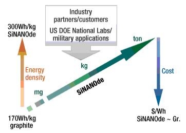
March 1, 2011 – Nanosys’ process-ready silicon composites (SiNANOde, Fig 1.) increase lithium ion (Li-ion) battery cell capacity without compromising cycle life. Yimin Zhu, director, battery & fuel cell, at Nanosys, recently spoke at the IEEE Bay Area Nanotechnology Council lunch forum (2/15/11, Santa Clara, CA).

Click to Enlarge
Figure 1. SiNANOde system. SOURCE: Nanosys

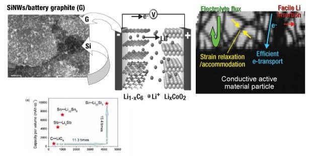
The SiNANOde nanomaterial deforms to fill void areas in the carbon anode material matrix and remains intact and fully functional after 100% DoD cycle testing. The technology also demonstrated a >2× capacity improvement using 10% additive in a Li+ battery anode. Nanosys is co-developing battery solutions with several of the world’s largest Li+ battery makers, noted Zhu. And volume revenue shipments are expected in 2011. Figure 2 shows the current status of the technology.

Click to Enlarge
Figure 2. SiNANOde technology status. SOURCE: Nanosys

In his presentation, Zhu noted how the value in the nanotechnology materials revolution is shifting to novel, tunable materials. “Architected materials not only can be processed using the mature means, but also allow the control of microstructure resulting in unique products,” said Zhu.

Click to EnlargeListen to Zhu’s interview: Download (iPhone/iPod users) or Play Now

In a podcast interview at the event, Zhu discusses details on how silicon nanocomposites are being used to accelerate the improvement in storage capacity of Li-ion cells with Debra Vogler, senior technical editor. He outlined how Nanosys was able to overcome some of the challenges in developing the microstructure of its architected materials for energy storage solutions. One of the capabilities the company developed was a new prototyping process, the goal of which was to develop a substrate-free growth process; Zhu describes the process.

Listen to another interview with Nanosys, this one about quantum dots, here.

Follow Small Times on Twitter.com by clicking www.twitter.com/smalltimes. Or join our Facebook group