Category Archives: LEDs

March 1, 2011 — A team led by Jan Schroers, a materials scientist at Yale University, has shown that some recently developed bulk metallic glasses (BMGs) — metal alloys that have randomly arranged atoms as opposed to the orderly, crystalline structure found in ordinary metals — can be blow molded like plastics into complex shapes that can’t be achieved using regular metal, yet without sacrificing the strength or durability that metal affords. The material is able to take on a seemingly endless variety of forms.

Click to Enlarge

Jan Schroers and his team have developed novel metal alloys that can be blow molded into virtually any shape.

"These alloys look like ordinary metal but can be blow molded just as cheaply and as easily as plastic," Schroers said. So far the team has created a number of complex shapes, including seamless metallic bottles, watch cases, miniature resonators, and biomedical implants. These shapes can be molded in less than a minute and are twice as strong as typical steel.

The materials cost about the same as high-end steel, Schroers said, but can be processed as cheaply as plastic. The alloys are made up of different metals, including zirconium, nickel, titanium and copper.

The team blow molded the alloys at low temperatures and low pressures, where the bulk metallic glass softens dramatically and flows as easily as plastic but without crystallizing like regular metal. It’s the low temperatures and low pressures that allowed the team to shape the BMGs with ease, versatility and precision, Schroers said. To carefully control and maintain the ideal temperature for blow molding, the team shaped the BMGs in a vacuum or in fluid.

"The trick is to avoid friction typically present in other forming techniques," Schroers said. "Blow molding completely eliminates friction, allowing us to create any number of complicated shapes, down to the nanoscale."

Schroers and his team are using their new processing technique to fabricate miniature resonators for microelectromechanical systems (MEMS) as well as gyroscopes and other resonator applications.

In addition, by blow molding the BMGs, the team was able to combine three separate steps in traditional metal processing (shaping, joining and finishing) into one, allowing them to carry out previously cumbersome, time- and energy-intensive processing in less than a minute.

"This could enable a whole new paradigm for shaping metals," Schroers said. "The superior properties of BMGs relative to plastics and typical metals, combined with the ease, economy and precision of blow molding, have the potential to impact society just as much as the development of synthetic plastics and their associated processing methods have in the last century."

Their findings are described online in the current issue of the journal Materials Today. Other authors of the paper include Thomas M. Hodges and Golden Kumar (Yale University); Hari Raman and A.J. Barnes (SuperformUSA); and Quoc Pham and Theodore A. Waniuk (Liquidmetal Technologies).

Learn more at www.yale.edu.

Follow Small Times on Twitter.com by clicking www.twitter.com/smalltimes. Or join our Facebook group

February 28, 2011 — Brewer Science Inc., advanced lithography materials supplier, launched the OptiStack system of products: a combination of materials, software and process support for advanced lithography. In tandem, Brewer Science debuted the ARC 300 coating series, designed to work with OptiStack.

Brewer Science’s OptiStack system offers variable n and k of the hardmask layer. The OptiStack modeling software allows for significant optimization of lithography conditions while maintaining the desired multilayer thicknesses so the customer can use existing optical proximity correction (OPC) and etch recipes.

The Brewer Science OptiStack include the broad resist compatibility of Brewer Science products, variable n and k materials that give the same lithography performance regardless of substrate by eliminating topography dispersion and underlying substrate optical constants from the OPC equation, ArF and KrF wavelength flexibility, a proprietary OptiStack simulation tool for advanced lithography process modeling, and process development support.

Brewer Science simultaneously debuted the ARC 300 coating series, a state-of-the-art ArF bottom anti-reflective coating (BARC) series designed to be optimized using OptiStack lithography simulation software. It suits various advanced ArF lithography processes and substrates with a single BARC platform.

Click to Enlarge

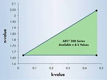
Figure. ARC 300 coating series optical property range.

The ARC 300 coating series allows for a range of n and k values in a single BARC platform. The material provides low reflectivities of less than 0.1% for various substrates and film thicknesses. The ARC 300 coating series can extend leading-edge ArF dry and immersion processes in single- and double-patterning lithography schemes.

Brewer Science will be at SPIE Advanced Lithography, taking place February 27 to March 3 in San Jose, CA, at Booth 225.

Brewer Science continuously improves leading-edge lithography products to reduce defectivity and outgassing and increase ease of line integration. The company develops materials, processes, and equipment for applications in semiconductors, advanced packaging/3D ICs, MEMS, displays, HB LEDs, and printed electronics. Learn more about Brewer Science at www.brewerscience.com.

Subscribe to Solid State Technology/Advanced Packaging.

Follow Solid State Technology on Twitter.com via editors Pete Singer, twitter.com/PetesTweetsPW and Debra Vogler, twitter.com/dvogler_PV_semi.

Or join our Facebook group

By Debra Vogler, senior technical editor

February 23, 2011 — As gold becomes more expensive, copper wire bonding becomes more appealing for chip packaging. Reverse bonding, fine-pitch bonding, looping, second bonds, and other technologies are ramping on roadmaps, according to Kulicke & Soffa (K&S).

Bob Chylak, VP engineering, packaging & process integration at Kulicke & Soffa, was the featured speaker at a recent iMAPS NorCal chapter lunch meeting (Santa Clara, CA; 2/2/11). He covered the topic of converting from gold to copper for wire bonding — a move gaining ever greater interest by the surging price of gold. With heightened activities to close the knowledge gap with respect to using copper, many of the challenges have been addressed, observed Chylak.

Listen to Chylak’s interview:  Download (iPhone/iPod users) or Play Now

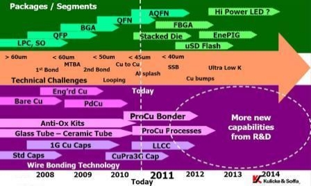
Laying out his company’s copper R&D roadmap (figure), Chylak noted that high-volume production of fine-pitch copper replacing gold already started in 2010. Advanced QFNs and stacked die still need to be developed, and LED packaging needs to be transitioned to copper, though Chylak noted that the challenge there will be with copper’s reflectivity not being as good as gold.

Click to Enlarge

Figure. Copper transition and roadmap planning. SOURCE: Kulicke & Soffa

Chylak said that nearly the entire K&S process engineering staff is working on the copper transition. In particular, work is being done on reverse bonding and getting yields to 50ppm or less. "It’s mainly around the looping [for stacked dies] and second bonds [including for LEDs] we’re focusing on," said Chylak.

Subscribe to Solid State Technology/Advanced Packaging.

Follow Advanced Packaging on Twitter.com by clicking www.twitter.com/advpackaging. Or join our Facebook group

Top articles on LEDs:

February 21, 2011 — At Strategies in Light in Santa Clara, CA, Solid State Technology editor-in-chief Peter Singer will lead a roundtable panel on manufacturing issues and strategies for LEDs, as part of "Transforming the LED & lighting markets." Attend the workshop Tuesday, February 22 from 8 to noon.

In order to fulfill the promise of large LED market penetration in a variety of applications ranging from LCD display backlights to general illumination, the cost of large-volume LED production must continually fall, both at the chip and packaged device level. Singer’s workshop will explore in depth the advances in LED manufacturing technology that will be needed to reduce the cost of HB LEDs. Topics to be addressed include:

  • The potential for process automation
  • Yield management
  • Metrology
  • Move to larger substrates
  • Adapting existing semiconductor facilities to LED
    manufacturing.

Speakers:

Click to EnlargeThomas Uhrmann, Business Development Manager, EV Group (EVG).
Thomas Uhrmann is business development manager for compound semiconductors and Si-based power devices at EV Group (EVG). In his current role, he is responsible to introduce and manage technological innovations for the fabrication of high-brightness light emitting diodes (HB-LEDs) at EVG. Uhrmann holds an engineering degree in mechatronics from the University of Applied Sciences in Regensburg, and a PhD in microelectronics from Vienna University of Technology. Uhrmann has authored and co-authored several papers on semiconductor diode structures, micro- or nanomagnetism and related areas.

Click to EnlargeChris Moore, President and CEO, Semilab AMS.
Chris Moore manages the US operations of Semilab that include Semilab USA and Semilab AMS, based in Billerica MA, and the Semilab SDI group in Tampa Florida. He is also a member of the Semilab Corporate management team. Semilab designs, manufactures, markets and sells optical metrology and contact and non-contact electrical characterization equipment for the semiconductor, PV and materials research markets. Chris is one of the co-chairs of SEMI’s HB-LED standards committee, currently co-chair of the SEMI PV Electrical and Optical Task Force, and co-chair of the recently formed 3D-ICs standards committee. As the VP technology of Waterloo Scientific, Chris helped develop compound semiconductor metrology equipment based on photoluminescence and high speed x-ray. When Waterloo Scientific was purchased by Philips, Chris became part of the Philips Analytical Waterloo and subsequently the Philips Boston management team. While with Philips Advanced Metrology systems Chris’s accomplishments include leading the design team which produced the MBIR infra-red reflectometry tool commonly used in the industry for 3D-IC etched structure metrology.

Click to EnlargeMike Plisinski, VP & General Manager, Rudolph Technologies Inc.
Michael (Mike) Plisinski has served as Rudolph Technologies’ Vice President and General Manager, Data Analysis and Review Business Unit, since February 2006 when the Company merged with August Technology Corporation. From 2003 to 2006, his positions at August Technology included Vice President of Engineering and Director of Strategic Marketing for review and analysis products. Prior to joining August, Plisinski was founder and President of Counterpoint Solutions, a semiconductor review and analysis company, later acquired by August Technology. He has a B.S. in Computer Science from the University of Massachusetts.

Click to EnlargeArdy Johnson, VP Corporate Marketing, Rudolph Technologies Inc.
Ardelle (Ardy)Johnson is currently Vice President of Marketing at Rudolph Technologies. In this capacity, he oversees the Product Management, Communications, Strategic Market Research and Process Applications groups. Johnson held this same position at August Technology for before its merger with Rudolph in 2006. Prior to his tenure with August, Johnson was employed by FSI International, Inc. for twenty-five years, serving most recently as Vice President. Johnson has a B.S. degree from the University of Minnesota and an MS degree from the University of Wisconsin.

Click to EnlargeRavi Kanjolia, CTO, SAFC Hitech
Dr. Ravi Kanjolia, is responsible for linking SAFC Hitech’s expertise in electronics materials, chemistry and delivery systems to applications across the microelectronics industries, as well as maintaining a steady product pipeline for the future. He is also directly responsible for the worldwide R&D of SAFC Hitech and its external academic/industrial collaborations. Dr. Kanjolia’s main research interest is in the field of MOCVD/ALD precursors for compound semiconductors and silicon semiconductors for the fabrication of future generation semiconductor devices. Prior to joining SAFC Hitech (formerly Epichem), Dr. Kanjolia rose through a series of research and managerial positions at Morton Metalorganics (now Dow). Prior to that, he was an Assistant Professor at the University of Alabama at Birmingham (UAB).

Click to EnlargeJames Brodrick, Lighting Program Manager, US Department of Energy
James Brodrick manages the U.S. Department of Energy Solid-State Lighting Program. Drawing on extensive technical and market knowledge, Dr. Brodrick has designed a comprehensive DOE strategy to move SSL from lab to market. The program comprises over 70 R&D projects, driving technology innovation and breakthroughs in efficiency and performance. Dr. Brodrick also has implemented a broad-based set of commercialization support strategies which closely coordinate with research progress to ensure proper application of SSL products and to avoid buyer dissatisfaction and delay of market development

Click to EnlargeWilliam Quinn, Chief Technologist, Veeco Metrology Inc.
William E. Quinn is Chief Technologist at Veeco MOCVD Operations. He has a BA in chemistry from Rutgers University and a Ph.D. in Material Science and Engineering from Stevens Institute of Technology. Prior to joining Veeco in 2004, he was engineering director at Skyworks solutions in Woburn, MA. Bill has been involved in research and production of III-V epitaxy materials for more than 25 years.

Moderator:

Peter Singer has been covering the semiconductor and related industries for more than 26 years. Now Editor-in-Chief of Small Times, Photovoltaics World, and Solid State Technology/Advanced Packaging, he was previously with Semiconductor International. He has authored more than 200 articles on all aspects of semiconductor manufacturing and related industries, including optoelectronics, photonics and photovoltaics. He has a degree in electrical engineering from the University of Illinois, Champaign-Urbana.


Subscribe to Solid State Technology/Advanced Packaging.

Follow Solid State Technology on Twitter.com via editors Pete Singer, twitter.com/PetesTweetsPW and Debra Vogler, twitter.com/dvogler_PV_semi.

Or join our Facebook group

Click to Enlarge

Thermal Technology’s Model K1 sapphire crystal grower
used for LED substrate production.

February 18, 2011 — Thermal Technology, crystal growth equipment and high-temperature furnace  manufacturer, recently received 59 orders for their Model K1 90kg sapphire crystal grower from customers in Taiwan, Korea and China. In total, these growers will produce 5.2 million two-in-equivalents (TIE) per year.

To satisfy the high demand of the rapidly growing sapphire market, Thermal Technology is shipping systems weekly. "I recently returned from our customer’s site in Taiwan where they ceremoniously unveiled a perfect 90 kg crystal grown in our K1 system," says Matt Mede, Thermal Technology president and CEO, adding that the customer owns 14 K1 systems for LED substrate production.

 No other domestic producer of sapphire crystal growth technology has machines in successful production, according to Mede, citing quality design, crystal size and tool capability. The Model K1 sapphire crystal grower advances beyond the traditional kyropoulos process. It is intended for LED substrate production with short cycle time.

Click to Enlarge
90 kg sapphire crystal grown in Thermal Technology Model K1 crystal grower.

Thermal Technology designs and manufactures crystal growing systems and high temperature vacuum and controlled atmosphere furnaces for the advanced processing of metals, ceramics, glass and quartz.

Sign up for SST’s free webcast, "Light and Color Measurement of Today’s LED Technology," sponsored by Konica Minolta Sensing Americas, on March 2.

Subscribe to Solid State Technology/Advanced Packaging.

Follow Solid State Technology on Twitter.com via editors Pete Singer, twitter.com/PetesTweetsPW and Debra Vogler, twitter.com/dvogler_PV_semi.

Or join our Facebook group

Veeco GaN MOCVD tool debut


February 17, 2011

By Debra Vogler, senior technical editor

February 17, 2011 — Veeco Instruments’ new TurboDisc MaxBright GaN MOCVD multi-reactor system is poised to take advantage of what the company believes is an accelerated rate of LED TV penetration (Fig. 1). According to Jim Jenson, VP of marketing at Veeco, who cited DisplaySearch/Veeco estimates in a podcast interview with SST, LED TV penetration is expected to reach 50% in 2011 and increase to ~80% in 2013, or perhaps sooner. Among the reasons LEDs are replacing LCD TVs that are backlit with CCFL technology are:

  • LEDs enable much thinner TVs and lower power consumption,
  • LEDs have better display characteristics (e.g., LEDs can do local dimming in direct-lit displays),
  • LEDs do not contain mercury, as do CCFLs.

Listen to Jenson’s interview: Download (iPhone/iPod users) or Play Now

Besides LED TVs, Jenson says many LED manufacturers are already positioning themselves to take advantage of the move to replace incandescent light bulbs and fluorescent tube lighting.

Click to Enlarge
Figure 1. LED TV opportunity. SOURCES: DisplaySearch Q4/10 and Veeco estimates.

The new system targets manufacturing of high-brightness LEDs (HBLEDs) and is capable of single- or multi-chamber layer growth; this allows for LEDs to be manufactured either serially (individual layers of LEDs can be grown sequentially in each reactor) or in parallel (the entire LED is grown on a per reactor basis). Two to four different reactors can be mounted around a central handler, which can handle a higher capacity carrier, and according to Jenson, each reactor can handle 20% more wafers than the previous generation.

Click to Enlarge Click to Enlarge
Figure 2. a) Within-wafer uniformity and b) Wafer-to-wafer uniformity.

An enabling feature of the tool is model-based temperature control, which uses a proprietary close-loop thermal control algorithm. Jenson explains that conventional closed-loop thermal control uses PID technology, which has a relatively slow settling time, taking a number of minutes for the temperature to stabilize after significant excursions. The new tool uses an algorithm that creates a 3D model in time of the entire thermal environment of the reactor; it requires about 500 differential equations being solved simultaneously every time there is a temperature change. "This results in very fast transitions, and very fast settling time between one temperature change and another," said Jenson. "We see a 5-10% throughout improvement."

According to Jenson, the tool has a >90% yield in a 5nm bin which means 90% of the LEDs on a platter, or 90% of the LEDs within a wafer, are within a wavelength range of 5nm (Fig. 2).  

Subscribe to Solid State Technology/Advanced Packaging.

Follow Solid State Technology on Twitter.com via editors Pete Singer, twitter.com/PetesTweetsPW and Debra Vogler, twitter.com/dvogler_PV_semi.

Or join our Facebook group
February 16, 2011 — Industry analyst firm NanoMarkets issued a report, "The Business Case for Indium Tin Oxide and Alternative Transparent Conductors," that addresses the viability of transparent conductor alternatives to indium tin oxide (ITO). NanoMarkets pegs the total transparent conductor market at slightly over $3 billion (USD) in revenues in 2011 and growing to over $10 billion in 2018. The market for alternatives to ITO will be worth almost $1.9 billion at that same time.

NanoMarkets’ new report notes that while materials costs are obviously crucially important to commoditized markets such as photovoltaics (PV) and displays, simply reducing BOM costs will not be enough of an impetus for display and other manufacturers to switch from ITO to alternative transparent conductors.

In this report, NanoMarkets examines the business case for using alternative transparent conductors in key applications including displays, lighting and photovoltaics. The materials considered are other TCOs, conductive polymers, nanosilver coatings, and nanocarbon coatings.

The report looks at the current and future performance factors of the major alternatives to ITO and compares them in quantitative terms to ITO then considers how these comparisons are likely to change over time, especially given the early technology stage, which is where transparent conducting nanomaterials currently reside. The principal factors include transparency, conductivity, flexibility/resiliency and cost in addition to other factors.

It also reviews the business cases that have been made in all the applications areas in which transparent conductors are used and how these are likely to evolve over the next few years as materials and end-user technologies change. In particular, NanoMarkets looks at how the arrival of next-generation displays, solid-state lighting and new types of solar panels are shifting the balance against ITO. The relative advantages of the various transparent conductors being offered are translated into cost savings and money making opportunities in each of the applications areas being considered.

"The Business Case for Indium Tin Oxide and Alternative Transparent Conductors" is the latest report from NanoMarkets that addresses the market opportunities within transparent conductors, both ITO and alternatives. The NanoMarkets report is part of its recent analyses of transparent conductor market opportunities in photovoltaics, displays, and OLEDs.

NanoMarkets tracks and analyzes emerging market opportunities in energy and electronics markets created by developments in advanced materials. Additional details are available at www.nanomarkets.net

February 15, 2011 – Marketwire — InVisage Technologies Inc., image sensor technology start-up, received its series C round of venture funding, led by Intel Capital. The undisclosed amount will be used to bring the company’s quantum-dot-based QuantumFilm technology and products into mass production.

Intel Capital joins InVisage’s existing investors RockPort Capital, InterWest Partners, OnPoint Technologies and Charles River Ventures.

QuantumFilm was developed by InVisage after research at the University of Toronto and at InVisage. The technology is based on quantum dots — semiconductors with unique light-capture properties. QuantumFilm works by capturing an imprint of a light image, and then using the silicon beneath it to read out the image and turn it into versatile digital signals. InVisage spent three years engineering the quantum dot material to produce highly sensitive image sensors that integrate with standard CMOS manufacturing processes.

The first application of QuantumFilm will enable high performance in tiny form factors, breaking silicon’s inherent performance-resolution tradeoff. Initially targeting cameraphone applications, which is the largest and fastest growing portion of the image sensor market, InVisage Technologies’ QuantumFilm will be sampling by summer, and could be in devices early next year.

"Image sensors for smart phones and handheld devices are a huge market opportunity and InVisage is well positioned to capture significant market share," says Dave Flanagan, managing director, Intel Capital. "InVisage is the first company in a while to think differently about image sensors and we are confident that its products will lead the imaging market on a new vector of innovation."

"The image sensor industry as a whole has focused entirely on increasing the number of pixels and has failed to see the big picture. As a result, there has been a lack of new ideas in the market for some time," says Jess Lee, CEO, InVisage Technologies. "InVisage’s QuantumFilm technology will bring stunning image quality and advanced new features."

InVisage Technologies, Inc. is a venture-backed fabless semiconductor company developing imaging-sensing technology that will replace silicon. More information is available at www.invisage.com.

Subscribe to Solid State Technology/Advanced Packaging.

Follow Advanced Packaging on Twitter.com by clicking www.twitter.com/advpackaging. Or join our Facebook group

February 11, 2011 – Marketwire — Palomar Technologies, precision microelectronics and optoelectronic packaging systems provider, will hold meetings at Stategies in Light to discuss its recent upgrades to high-brightness light emitting diode (HB-LED) assembly.

Strategies in Light will take place February 22-24 in Santa Clara, CA.

Worldwide account manager for Assembly Services, Steve Buerki, will be on site at the Strategies in Light conference at booth #238. Palomar is offering free admission passes to the Strategies in Light exhibitors’ show floor for attendees to speak with Buerki.

Precision Microelectronics Assembly Services (Assembly Services) is the contract assembly division of Palomar Technologies. Assembly Services provides prototyping, test, measurement and production for high accuracy and complex wire and die attach applications. Additional clean room space was recently added in the California-based laboratory, increasing production capacity by 50%. Assembly Services expertise includes development and production for applications such as HB LEDs, RF power modules, military hybrids and laser diode packages.

Palomar Technologies, a former subsidiary of Hughes Aircraft, provides die attach solutions, wire bonding equipment, optoelectronic packaging systems and contract assembly services. For more information, visit www.palomartechnologies.com.

Subscribe to Solid State Technology/Advanced Packaging.

Follow Advanced Packaging on Twitter.com by clicking www.twitter.com/advpackaging. Or join our Facebook group

February 10, 2011 — Nanolasers grown directly on a silicon surface could be a starting point for better microprocessors, biochemical sensors, and other optoelectronic products. UC Berkeley researchers grew nanopillars made of indium gallium arsenide, a III-V material, onto a silicon surface at 400°C.

The researchers point out that marrying III-V with silicon to create a single optoelectronic chip has been problematic. The atomic structures of the two materials are mismatched.

"Growing III-V semiconductor films on silicon is like forcing two incongruent puzzle pieces together," said study lead author Roger Chen, a UC Berkeley graduate student in electrical engineering and computer sciences. "It can be done, but the material gets damaged in the process."

Click to Enlarge
Figure 1. Shown is a schematic (left) and various scanning electron microscope images of nanolasers grown directly on a silicon surface. The achievement could lead to a new class of optoelectronic chips. (Courtesy Connie Chang-Hasnain Group)

Moreover, the manufacturing industry is set up for the production of silicon-based materials, so for practical reasons, the goal has been to integrate the fabrication of III-V devices into the existing infrastructure, the researchers said.

"Today’s massive silicon electronics infrastructure is extremely difficult to change for both economic and technological reasons, so compatibility with silicon fabrication is critical," said the study’s principal investigator, Connie Chang-Hasnain, UC Berkeley professor of electrical engineering and computer sciences. "One problem is that growth of III-V semiconductors has traditionally involved high temperatures — 700°C or more — that would destroy the electronics. Meanwhile, other integration approaches have not been scalable."

The UC Berkeley researchers overcame this limitation by finding a way to grow nanopillars made of indium gallium arsenide, a III-V material, onto a silicon surface at the relatively cool temperature of 400°C.

“Working at nanoscale levels has enabled us to grow high quality III-V materials at low temperatures such that silicon electronics can retain their functionality,” said Chen.

The researchers used metal-organic chemical vapor deposition (MOCVD) to grow the nanopillars on the silicon. "This technique is potentially mass manufacturable, since such a system is already used commercially to make thin film solar cells and LEDs," said Chang-Hasnain.

"This is the first bottom-up integration of III-V nanolasers onto silicon chips using a growth process compatible with the CMOS technology now used to make integrated circuits," said Chang-Hasnain.

Click to Enlarge

Figure 2. The unique structure of the nanopillars grown by UC Berkeley researchers strongly confines light in a tiny volume to enable subwavelength nanolasers. Images on the left and top right show simulated electric field intensities that describe how light circulates helically inside the nanopillars. On the bottom right is an experimental camera image of laser light from a single nanolaser. (Courtesy Connie Chang-Hasnain Group)

Once the nanopillar was made, the researchers showed that it could generate near infrared laser light (about 950nm wavelength) at room temperature. The hexagonal geometry dictated by the crystal structure of the nanopillars creates a new, efficient, light-trapping optical cavity. Light circulates up and down the structure in a helical fashion and amplifies via this optical feedback mechanism.

The researchers describe their work in a paper published in the journal Nature Photonics. Access it here: http://www.nature.com/nphoton/journal/vaop/ncurrent/full/nphoton.2010.315.html

The unique approach of growing nanolasers directly onto silicon could lead to highly efficient silicon photonics, the researchers said. They noted that the miniscule dimensions of the nanopillars — smaller than one wavelength on each side, in some cases — make it possible to pack them into small spaces with the added benefit of consuming very little energy.

"Our results impact a broad spectrum of scientific fields, including materials science, transistor technology, laser science, optoelectronics and optical physics," said Chang-Hasnain. "Ultimately, this technique may provide a powerful and new avenue for engineering on-chip nanophotonic devices such as lasers, photodetectors, modulators and solar cells," said Chen.

In the future, the researchers expect to improve the characteristics of these lasers and control them electronically.

The Defense Advanced Research Projects Agency and a Department of Defense National Security Science and Engineering Faculty Fellowship helped support this research.

Courtesy of Sarah Yang, Media Relations, UC Berkeley