Tag Archives: Small Times Magazine

May 12, 2010 – Researchers have come up with a way to calculate and manipulate the effects of Casimir forces, and then use them to keep microelectromechanical systems (MEMS) components from sticking together, which could greatly reduce failure rates and enable new, more affordable devices.

Casimir forces, discovered more than 60 years ago, are quantum forces affecting objects at miniscule distances. At such tiny dimensions, a number of particles flash in and out of existence, with interactions that generally balance out — but at extremely close distances Casimir forces apply to attract particles together. In the 1960s researchers figured out a formula to theoretically describe the effects of Casimir forces on tiny objects, but stopped short of actually solving and evaluating such interactions except for a few examples (e.g. two parallel plates, or more recently a plate and cylinder).

Now, researchers from MIT say they have come up with a way to solve Casimir-force equations for any number of objects with conceivable shape. Their work is published in the Proceedings of the National Academies of Sciences (PNAS). Essentially, effects of Casimir forces on objects <100nm apart can be precisely modeled using objects both 100,000× bigger and further apart that are immersed in a conductive fluid, by calculating the strength of an electromagnetic field at various points around the objects.

"Analytically, it‚s almost impossible to do exact calculations of the Casimir force, unless you have some very special geometries," according to Diego Dalvit, a specialist in Casimir forces at the Los Alamos National Laboratory, in a statement. In principle, the technique, however, "can tackle any geometry. And this is useful."

Very useful, in fact, for MEMS devices, where attractive Casimir forces can cause moving parts to stick together and stop working properly. Earlier this year, the MIT researchers in collaboration with Harvard described an arrangement of materials that enable Casimir forces to cause repulsion in a vacuum. MEMS device design would still require intuition of certain geometries and their properties, though, to know where such repulsion could occur, Dalvit notes.

Note that last year a Harvard-led group examined Casimir forces and how to change the attractive force into a repulsive one — but that work focused on known repulsion for objects in fluids, while the new MIT-led work is about the unexplored area of vacuum-separated objects, explains MIT paper’s lead author Alex Rodriguez. "The ability to obtain Casimir repulsion between vacuum-separated objects was not known and is the subject of much on-going research in this field — as a matter of fact, many scientists believed it was impossible, including myself," he tells Small Times.

Click to Enlarge
Though negligible at larger scales, Casimir forces can cause moving parts of micromachines to stick together. (Image: Sandia National Laboratories, MIT)


May 11, 2010 – Researchers from Georgia Tech and the National Institute of Standards and Technology (NIST) have developed methods to more accurately measure the length of nanopores in membranes, seen as a first step in calibrating tailor-made versions for applications such as rapid DNA analysis.

Single-nanometer-scale pores in thin membranes could act as "miniature analysis labs" for detecting and characterizing biological molecules, e.g. DNA or toxins, as they pass through or block the passage. Such systems could fit on a microchip (e.g., microfluidics — with more precise knowledge of the nanopore’s dimensions and structural features.

Their work, described in the Journal of Chemical Physics, involved drilling nanopores into a bilayer sheet of lipid molecules similar to membranes found in animal cells. Applying voltage across the membrane wall forced charged molecules (e.g., single-strand DNA) into the nanopore; as it passed into the channel, the ionic current flow reduces for a time that is proportional to the size of the chain — thus, its length can be derived.

The scientists also developed two ways of measuring these nanopores.

If a chain is long enough to reach the nanopore’s "pinch point," the force of the electrical field behind it will push the molecule through the rest of the channel. Exploiting this feature, the scientists developed a DNA probe method to measure distances from the openings on either side of the membrane to the pinch point — and adding them together gives the entire length of the nanopore. The probe method involved DNA strands of known length with a polymer sphere on one end; the aforementioned force that would push the strand through the pinch point now lodges the sphere in place with the DNA chain extending into the channel, and defines the distance to the pinch point. (If the chain is shorter than the pinch-point distance it is bounced out of the nanopore.)

Another way they devised to measure the length of the nanopore is dubbed the "single lollipop" method. Polymer molecules circulating in the solution collect on the inner side of the membrane; polymer-capped DNA probes of different length are forced one at a time into the nanopore from the opposite side. Probes with a DNA chain long enough to traverse the entire channel will affix to a free polymer molecule, thus defining the channel’s length. This "ice fishing" method also provides insight into the nanopores’ structure, by mapping the DNA chain’s voltage changes to the changing shape of the channel as it winds its way through.

Click to Enlarge
How the "ice fishing" method determines the distance across a membrane nanopore. DNA strands of known lengths topped by a polymer cap (orange sphere) are driven through the nanopore. Strands long enough to completely transverse the channel (left) will "hook" a circulating polymer (green sphere) on the other side of the membrane, and define the nanopore’s length. If not long enough, the DNA probe will bounce out of the pore (right). (Credit: J. Robertson, NIST)

May 4, 2010 – Researchers at North Carolina State University have developed a computer chip that can store an entire library’s worth of information using "magnetic nanodots."

In the work, discussed as an invited paper at the recent MRS Spring Meeting by prof. Jay Narayan, focuses on self-assembled nanodots (e.g. Ni, Ni-Pt, Fe-Pt), a process found to be extendable from 2D to 3D structures. The ≤6nm-dia. nanodots, made from single defect-free crystals, integrated directly onto a silicon chip and precisely oriented in the same way. Each nanodot stores one bit of information; a nanodot-infused chip could be capable of storing over a billion pages of information in a square inch.

Narayan’s work in self-assembly and epitaxial nanoparticles goes back several years, in papers published in Applied Physics Letters (e.g., this one from 2008).

NC State says the chips with which the nanodots are integrated "can be manufactured cost-effectively." The next step is to devise magnetic packaging for these integrated chips, e.g. using something like laser technology that can effectively interact with the nanodots.

April 28, 2010 – Researchers from the US and Europe say they have created devices with carbon nanotube (CNT) that can act as membranes for air filters far more effective than current ones.

The showerhead-resembling devices were created by chemical vapor deposition (CVD) of silicon dioxide templates, with laser-created holes; after 30min in the furnace the holes fill up with carbon nanotubes, through which only nanoscale objects can pass.

Click to Enlarge
Nanotube-infused microdevices, with forests of carbon nanotubes grown inside pores, can act as filters or as a carrier for improved catalysts. (Source: Rice U.)

"The basic idea is you have this carbon nanotube forest," explains Robert Vajtai, a Rice faculty fellow in mechanical engineering and materials science, in a statement. "The gas flows through, and because of the very small distance between the tubes, gas atoms have to hit many of them before they get out the other side."

This interaction lays the "scaffolding" for a catalyst template. When the CNTs are functionalized with catalytic chemicals, particles entering on one side of the filter come out the end in a different form — e.g., like an automobile catalytic converter, which turns carbon monoxide into carbon dioxide/nitrogen/water. In tests, Rice researchers deposited palladium onto the CNTs and used them to turn propene into propane (a benchmark test for catalysis), finding that the activated membranes "showed excellent and durable activity."

As a filter, the CNT-enabled membrane achieved 99% extraction of <1μm particles, removing about 100× more nanoparticles from laboratory air than the material used in high-efficiency particulate-absorbing (HEPA) filters, they note. The length of the CNTs (and thus density in the membrane) determines the filters’ permeability.

Results of the work were published in the journal ACS Nano.

Click to Enlarge
Nanotubes grown in holes in silicon dioxide wafers have the potential
to outperform currently available filters for many uses. (Source: Rice U.)

by Debra Vogler, senior technical editor

April 28, 2010 – FEI Company has introduced its Helios NanoLabx50 DualBeam Series (450(S) and 650) that integrates the company’s extreme high-resolution scanning electron microscope (XHR SEM) with a new, high-performance focused ion beam (FIB). Applications for the new system include failure analysis, 3D nanoscale characterization, prototyping, etc., in semiconductor and materials science R&D.

Key to the system’s SEM capabilities is being able to use low voltage (i.e., a more surface-sensitive beam) while achieving a high-resolution image. Degradation of resolution when going to a lower beam energy is avoided by using a monochromator (introduced two years ago) in the XHR SEM, which reduces the energy distribution at the source (i.e., less of a chromatic aberration effect), according to Richard Young, technology manager in FEI’s electronics group. So the spot size of the beam is "tightened" by using a narrower range of electron energies, resulting in a higher resolution, surface-sensitive beam (i.e., at 1kV). In effect, he explained, there is a tradeoff between penetration depth of the electrons and their surface sensitivity.

Click to Enlarge
 Click to EnlargeClick to Enlarge
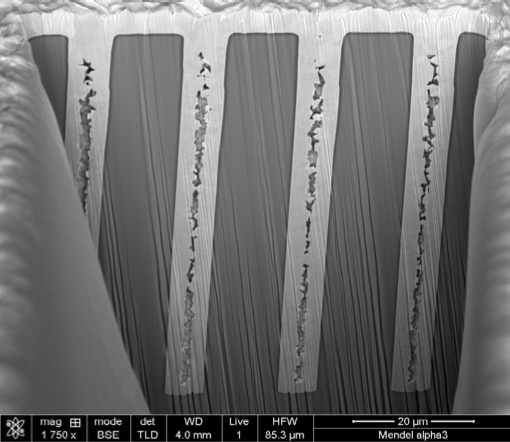
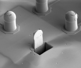
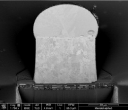
Figure 1. TSV and interconnect applications. (Source: FEI Co.)

The XHR SEM imaging is capable of sub-nanometer imaging from 30kV down to 1kV and <1.2nm at coincident WD. Through-silicon vias (TSV) and interconnect applications are challenging because of the increased milling time required for the larger structures. To address this issue, the company’s Tomahawk FIB, which was improved with a fast-switching technology, provides SEM and FIB live monitoring of milling operations, a smaller FIB spot for more precise milling control, and higher beam currents for faster material removal on large structures, such as TSVs (Figure 1). According to Todd Templeton, product marketing manager at FEI, overall throughput of advanced TEM lamella preparation has been improved by 40%. The FIB column is capable of maximum material removal rates at 65nA. In the TSV structures shown in Fig. 1a, a TSV that was 60-80μm deep would take ~12hrs to mill the volume away with the previous tool; with the new tool, however, the time is~4 hrs.

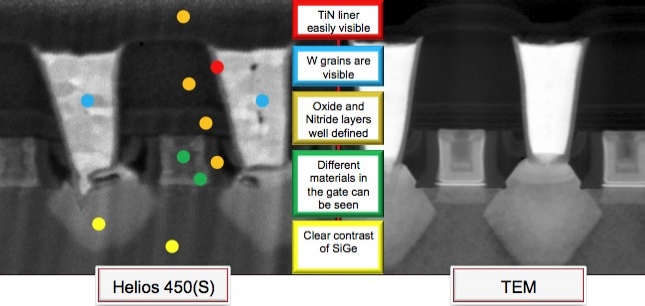
Templeton also told SST that the improved materials contrast of the new platform enables end-users to find defects in cross-sections using the SEM that previously might have to be examined using TEM. "The SEM image (Figure 2, left image) is good enough for many applications for finding defects and process issues," explained Templeton, so "there is no need to go to a TEM image (Fig. 2, right image)." This is beneficial because acquiring the SEM image takes less time than generating a TEM image. However, when a TEM image is required, the new system is capable of handling a higher volume of samples.

Click to Enlarge
Figure 2. Improved materials contrast in cross-section. (Source: FEI Co.)


April 26, 2010 –  A new nanopatterning technique demonstrated by IBM can achieve ≤15nm resolutions, and could supplant e-beam lithography in applications ranging from CMOS to self-assembled nanoscale objects, and for materials including "molecular glass."

The work by IBM scientists in Zurich, described in recent papers in Science and Advanced Materials, describes a new technique that applies a tiny silicon tip with sharp apex (500nm-long, a few nm at the apex) to create patterns and 3D structures. Demonstrating the technique’s capabilities, the team created several 3D patterns each on a different material:

  • a 25nm high 3D replica of the Matterhorn, built in "molecular glass," to 1:5 billion scale;
  • a complete 3D map of the world (22×11μm), carved into a polymer, and built out of 500,000 20nm2 pixels, and created in 143 seconds;
  • a 2D-sized IBM logo, etched 400nm deep into silicon, to demonstrate the technique’s viability for nanofabrication; and
  • a 2D high-resolution 15nm dense line patterning.

The silicon tip, similar to those used in atomic force microscopes (AFM), is attached to a bendable cantilever that controllably scans a substrate surface, with 1nm accuracy. Applying heat and force removes substrate material in predefined patterns — akin to a "nanomilling machine," IBM says. Modulating the force or readdressing individual spots removes more material to create complex 3D structures. (For the Matterhorn nanosculpture, 120 individual layers of molecular glass were removed.)

Close-up of the nanoscale silicon tip. Measuring 500nm in length and only a few nanometers at its apex, it is attached to a cantilever that controllably scans the surface of the substrate material with 1nm accuracy. By applying heat and force, the nano-sized tip can remove substrate material based on predefined patterns. (Image courtesy of IBM Research-Zurich)

The technique’s precision enables resolutions down to 15nm and smaller — making it comparable to and actually more extendable than e-beam lithography, at one-fifth to one-tenth the cost and far less complexity, IBM notes.

A key development in crafting those nanosculptures was choosing the right materials to carve up. IBM points to its use of the technique in two materials: a polymer (polyphthalaldehyde) and a "molecular glass" similar to conventional resists used in nanomanufacturing. "The material was a ‘make it or break it’ issue," according to Jim Hedrick, scientist at IBM Research-Almaden. "We had to find and synthesize materials which form mechanically tough glasses and yet can be easily thermally decomposed into non-reactive volatile units."

The molecular glass into which the nano-Matterhorn was sculpted — a material first proposed in the 1990s by Yamagata U.’s Mitsuru Ueda in Japan for high-resolution photoresist (more recently applied by Cornell U.’s Chris Ober) — consisted of nearly spherical 1nm-sized snowflake-like molecules; tip temperatures of >330°C were required to break their hydrogen bonds and make them mobile to escape the surface. Patterned molecular glass has interest in its ability to be transferred by conventional etching techniques to silicon, for use in semiconductor manufacturing.

A 25nm-high replica of the Matterhorn peak, representing 1:5 billion scale (1nm = 57 altitude meters). 120 layers of material removed to create the 3D replica. (Image courtesy of Science/AAAS)

The polymer polyphthalaldehyde, used to create the 3D world map, was originally developed by IBM Fellow Hiroshi Ito in the 1980s. Exposure to high temperatures makes the polymer’s organic molecule fall apart into volatile pieces; a self-amplified reaction causes it to decompose and accelerates the patterning process by being even faster than the mechanical motion of the tip, the researchers explain.

(a) A 22×11nm 3D map of the world, "written" into a 250nm-thick polymer (scale: 8nm = 1000m altitude), composed of 500,000 pixels with 20nm pitch. White arrows in (b) and c) subareas indicate positions with features of 1 and 2 pixels widths, respectively, in the original bitmap. (d) Cross-section profiles along dotted line shown in (a), cutting from the Alps through the Black Sea, Kaukasian mountains, and Himalayas, with original data (blue) and relief reproduction (green). (Image courtesy of Advanced Materials)

April 23, 2010 – The National Institute of Standards and Technology (NIST) is opening up a competition with $25M in funding on the table for those who have the best ideas for research in materials to support "process-based industries" such as biomanufacturing.

The new Technology Innovation Program (TIP), which is offering $25M for first-year funding (expecting 25 new projects), is soliciting research proposals of "innovative research" in three areas:

  • Process scale-up, integration and design for materials advances;
  • Predictive modeling for materials advances and materials processing; and
  • Process advances that "dramatically improve" new materials processing, or resolve bottlenecks/inefficiencies in production of existing materials.

Efficiently moving new materials from lab to production environments and then market-readiness is a major challenge for manufacturers. Improving critical manufacturing processes to reduce costs, save time, increase quality, or reduce waste are thus key to competitiveness for process-based industries such as biomanufacturing (e.g. biopharmaceuticals, including vaccines), chemical production, and fuel producers.

Proposals for the NIST 2010 TIP competition are due by midnight (EST) on July 15, either submitted through grants.gov (search for "Catalog of Federal Domestic Assistance (CFDA) program 11.613" or "Funding Opportunity Number TIP-2010-B01") or sent by snail-mail. Additional details on the 2010 competition, including dates and locations of three "Proposers’ conferences" offering general information, are on the NIST Web site.

April 21, 2010 – Mitsubishi Heavy Industries (MHI) says it has delivered its first automated room-temperature bonding system for 200mm wafers to a MEMS manufacturer in Japan, the tool‘s first use in production.

The company’s MWB-08A tool incorporates a 20-wafer cassette (10 pairs) with fully automated wafer transfer and alignment. Bonding conditions are programmed for each wafer set, offering flexibility for small-lot production of various products. The tool’s functionality is compatible with earlier 150mm machines, so an upgrade path is available.

The tool transfer also includes MHI’s "Bonding Support Program," which liaises the company’s engineers and facilities with the customer to help support device development in applying room-temperature wafer bonding at each development stage: from conceptual design to functional prototype production to trial and mass production.

Room-temperature bonding activates the substrate surface with ion beam irradiation in a vacuum. Conventional wafer bonding applies heat; eliminating this step removes heat stress and strain, enabling rigidity and reliable bonding, and reduces cycle time (no heating/cooling cycle), the company explains. The end result is "significantly shorter production time," higher yields, and ultimately lower device production costs.

April 19, 2010 – Fujitsu Labs and Germany’s Technische Universität München (TUM) say they have developed a new biosensor technology that uses DNA movement to detect proteins.

The technology works by inducing a cyclical motion in negatively charged DNA and measuring its movement, enabling quick detection of proteins — accurately measuring proteins in 1/100th the time of previous methods, the groups claim.

Scientific and biological research continues to progress with identification of proteins causing ailments such as diabetes and cancer. Being able to more quickly detect the type, amount, and size of proteins enables earlier discovery of diseases, and more accurate and timely treatments.

Conventional methods to detect such proteins involve a multistep process requiring not insignificant quantities of samples (e.g., blood) for testing, and time and costs are high.

The new technology takes advantage of a DNA’s negative charge when in an aqueous solution. An electrode is cycled between positive and negative charges, which alternately attracts and repels the DNA. A fluorescent dye applied to the ends of the DNA allows them to act as reference points, shining when the DNA is repelled from the electrode and dimly lit when attracted to it — thus the movement of the DNA is made visible. (In addition to the graphic below, a video describes the process.)

Click to Enlarge
Enabling visibility of DNA movement. (Source: Fujitsu Labs.)

Molecules predisposed to bond strongly with the target protein are attached to the ends of the DNA where the dyes were applied. Once the two are bonded, the DNA’s movement is impeded by the molecules, enabling researchers to see the presence (or absence) of the target protein as well as how much has bonded. Rapidly cycling the electrode’s positive and negative charges can derive the bonded protein’s movement, and shape/size of the protein.

The biosensor technology can accurately measure proteins in 1/100th the time required with existing methods, and requiring only 1/100th the sample volume. And because it can not only detect the presence of proteins but also measure their size, it achieves superior precision, and applicability in a wider range of fields, the researchers say.

The TUM researchers, supported by Fujitsu Labs, aim to commercialize the technology through the German government’s "EXIST" incubator program; business plans based on the technology won recent German business plan competitions.

April 15, 2010 – Researchers from Lawrence Berkeley National Labs say they have taken a big step forward in addressing one of the major challenges in graphene: figuring out an economical, high-quality and production-worthy way of making it.

Graphene’s unique properties are well known: excellent electron mobility (100× faster than silicon) and an atomic structure with great flexibility and mechanical strength. But manufacturability is a problem — current fabrication methods based on mechanical cleavage or ultrahigh vacuum annealing aren’t compatible with volume production, notes Yuegang Zhang, materials scientist at Berkeley Labs. "Before we can fully utilize the superior electronic properties of graphene in devices, we must first develop a method of forming uniform single-layer graphene films on nonconducting substrates on a large scale," he says.

In their work, published in Nano Letters, Zhang and colleagues used direct chemical vapor deposition (CVD) to synthesize single-layer films of graphene on a dielectric substrate (they evaluated single-crystal quartz, sapphire, fused silica, and silicon oxide). Hydrocarbon precursors were catalytically decomposed over thin copper films (100-450nm thickness) which were predeposited via e-beam evaporation on the dielectric substrate. Dewetting and evaporating the Cu films yielded single-layer graphene film on a bare dielectric. Scanning Raman mapping, spectroscopy, and SEM and AFM confirmed continuous single-layer graphene films coating metal-free areas of dielectric substrate, measuring "tens of square micrometers."

Click to Enlarge
Figure 1. To make a graphene thin film, Berkeley researchers (a) evaporated a thin layer of copper on a dielectric surface; (b) then used CVD to lay down a graphene film over the copper. (c) The copper dewets and evaporates leaving (d) the graphene film directly on the dielectric substrate.

"This is exciting news for electronic applications because chemical vapor deposition is a technique already widely used in the semiconductor industry," Zhang notes.

Improved control of the dewetting and evaporation could lead to direct deposition of patterned graphene for large-scale electronic device fabrication, and could be used to deposit other 2D materials such as boron nitride, according to Zhang. And although wrinkles in the graphene film following the dewetting shape of the copper introduce mobility-slowing strains, "if we can learn to control the formation of wrinkles in our films, we should be able to modulate the resulting strain and thereby tailor electronic properties," he said.

Moreover, observing the films after Cu evaporation will help the researchers learn more about growth of graphene on metal catalyst surfaces, which will help inform better control of the process, leading to ways to tailor the film properties or produce different morphologies, such as graphene nanoribbons, he added.

Click to Enlarge
Figure 2. (a) Optical image of a CVD graphene film on a copper layer showing the finger morphology of the metal; (b) Raman 2D band map of the graphene film between the copper fingers over the area marked by the red square on left. (image from Yuegang Zhang)