Tag Archives: Small Times Magazine

June 8, 2011 – BUSINESS WIRE — The US Court of Appeals for the Federal Circuit affirmed the US International Trade Commission’s (ITC) final determination that MEMS Technology Berhad’s (MemsTech) importation and sale of certain MEMS microphone packages infringes Knowles Electronics LLC’s US Patents 7,242,089 and 6,781,231.

The Court of Appeals held that Knowles’s patents are valid and enforceable, and affirmed the ITC’s exclusion order barring MemsTech from importing its infringing products into the U.S.

The patents in this case are part of a large portfolio of patents related to Knowles SiSonic MEMS microphones  and microphone packaging technology. These patents cover several variations of SiSonic microphones and manufacturing methods.

Knowles designs and manufactures advanced acoustic components and MEMS microphones for major cell phone companies and consumer electronic devices. Knowles is owned by the Dover Corporation. For more information, visit www.knowles.com.

Knowles was recently on the other end of a patent dispute, when the ITC found that Knowles MEMS microphones infringed on Analog Devices Inc.’s (ADI) patents.

Subscribe to our MEMS Direct newsletter

June 8, 2011 — University of Pennsylvania researchers formed biological molecules connected to electrodes, paving the way for direct biological integration into electronic circuits. The team also developed a new microscope technique to measure the electrical properties of these constructs.

Click to Enlarge

Protein assemblies rendered under an atomic force microscope. Image reprinted with permission from "Direct Probe of Molecular Polarization in De Novo Protein–Electrode Interfaces," Kendra Kathan-Galipeau, Sanjini Nanayakkara, Paul A. O’Brian, Maxim Nikiforov, Bohdana M. Discher, Dawn A. Bonnell, ACS Nano, Copyright 2011 American Chemical Society.

Researchers arranged artificial proteins, bundles of peptide helices with a photoactive molecule inside, on electrodes. When light hit the proteins, they converted photons into electrons and passed them to the electrode. The mechanism is similar to "what happens when plants absorb light," said Dawn Bonnell, Trustee Chair Professor and director of the Nano/Bio Interface Center, "in this case, we want to use the electron in electrical circuits."

Until now, light-reactive peptide assemblies could not be measured for their ambient electrical properties, particularly capacitance. To build bio-circuit-based devices, these properties must be quantified, said Bonnell, noting the lack of understanding in this area: "We didn’t know what happens to electrons on dry electrodes with these proteins; we didn’t even know if they would remain photoactive when attached to an electrode."

Silicon-based circuits are easier to design, based on decades of Si use in electronics, and the inherent ease of working with one element rather than complex proteins. The researchers devised a method to measure protein properties, using a new kind of atomic force microscope technique, torsional resonance nanoimpedance microscopy. It uses a metallic tip and oscillating electric field to measure complex interactions and properties.

The researchers also decided to fabricate the photovoltaic proteins as they might eventually be incorporated into devices in open-air, everyday environments, rather than in a chemical solution. Assistant professor Bohdana Discher of the Department of Biophysics and Biochemistry at Penn’s Perelman School of Medicine, with a team, designed the self-assembling proteins then stamped them onto sheets of graphite electrodes.

Applications for the design include biosensors and photovoltaics. Instead of reacting to photons, proteins could be designed to produce a charge when in the presence of a certain toxins, either changing color or acting as a circuit element in a gadget.

The research was conducted by Dawn Bonnell, graduate students Kendra Kathan-Galipeau and Maxim Nikiforov and postdoctoral fellow Sanjini Nanayakkara (Department of Materials Science and Engineering in Penn’s School of Engineering and Applied Science). They collaborated with assistant professor Bohdana Discher of the Department of Biophysics and Biochemistry at Penn’s Perelman School of Medicine and Paul A. O’Brien, a graduate student in Penn’s Biotechnology Masters Program.

Their work was published in the journal ACS Nano (http://pubs.acs.org/doi/abs/10.1021/nn200887n)

This research was supported by the Nano/Bio Interface Center and the National Science Foundation.

Subscribe to our MEMS Direct newsletter

by Dr. Paula Doe, SEMI Emerging & Adjacent Markets

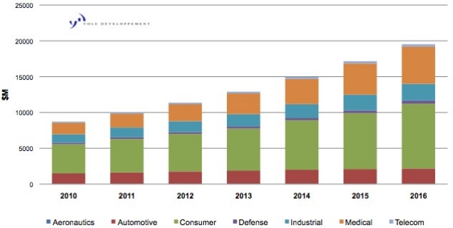
June 7, 2011 – Rapid growth in mainstream consumer markets is changing the structure of the MEMS industry from an artisanal to a volume manufacturing business. Yole Développement projects the MEMS market will near the $10 billion level this year, and is poised for 14% compound annual growth for the next five years, to approach close to $20 billion by 2016.

Click to Enlarge
MEMS forecast per application. (Source: Yole Développement)

These volume markets demand more efficient, non-artisanal solutions for moving designs into production. At the same time, with the maturing of the basic manufacturing technology, the value is moving from the device to the function and the system. And all these developments create a new set of challenges and opportunities to companies to find better ways to speed the ramp to low-cost volume production, to find better ways to integrate multiple die and software into easy-to-manufacture and easy-to-use functions, and to find the right business models to best use these skills to succeed.

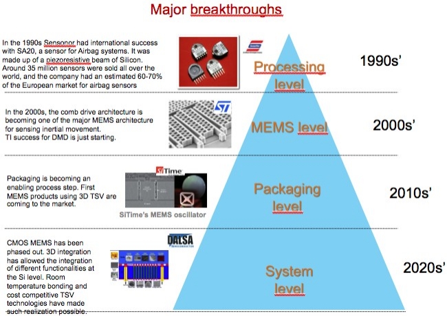
There has been a steady evolution over time, notes Yole founder and CEO Jean Christophe Eloy, as the young MEMS industry has matured to delivering higher functionality, from the manufacturing of MEMS structures in the 2000s, to the more recent innovations in integrated packaging. Coming next will be innovations in wafer bonding and through-silicon via (TSV) integration of multiple sensors and controls, requiring both packaging expertise for the integration and software expertise for managing the complex sensing and actions to be useful — raising the question of who in the value chain will do these steps.

Click to Enlarge
30 years of MEMS manufacturing history, an evolution aimed at climbing the value chain
toward increasing functionalities at the system level. (Source: Yole Développement)

The demand for rapid ramp to high-volume production is driving manufacturers to focus increasingly on ways to more efficiently re-use established process stacks or technology platforms or even product platforms for the more efficient development of new products. And the need to reduce cost for consumer products is driving a relentless push to smaller die size, and to integration by TSV or wafer bonding when possible, and to solutions like capping the MEMS with the ASIC or making use of SOI to form the cavity, says Eloy.

GlobalFoundries’ Rakesh Kumar, director of MEMS, argues that there’s big potential to apply an IC foundry’s best known methods and practices — worked out after many years of experience in semiconductor tools and technologies — toward the more efficient manufacturing of MEMS. To be successful, an IC foundry must lower costs, offer high yield and high-performance MEMS products in a manner similar to ICs, while also shortening time-to-market by reduced technology transfer time and fast ramp to production, he says.

Specialty MEMS foundries are also developing solutions. Claude Jean, EVP/GM at Teledyne DALSA Semiconductor, suggests that the traditional MEMS approach of developing products first on lab equipment then porting over to manufacturing tools is too slow for fast ramp to yields and fast cost reduction. Instead, he highlights the advantages of doing the final rounds of development with an infrastructure closer to production tools.

IMEC’s Jo De Boeck, SVP of smart systems and energy technology, suggests that MEMS technology platforms are required, supported with a design environment consisting of a reference tool flow, corresponding models and design kits and a basic design IP library. Moreover, successful product innovation implementation will require co-developing software and hardware into optimal systems solutions.

We’ve invited these speakers representing leading companies from different viewpoints across the value chain — as well as ones from major IDM Robert Bosch and startup Sand9 — to discuss these key industry issues at SEMICON West, Tuesday, July 12 ("The Future of MEMS". Right afterwards, for a more hands-on look at the future of MEMS, the MEMS Industry Group presents a demo zone of next-generation MEMS sensors in action, demonstrated by MEMS folks who can give the inside scoop on how they work.

Tuesday afternoon also features a related program focusing on packaging issues for heterogeneous integration of MEMS and CMOS. Microsoft’s GM of packaging, quality and reliability, Raj Master, will give the technical keynote, followed by an update on market trends from TechSearch International and IHS iSuppli, and a panel discussion including Fraunhofer IZM, Toshiba Corp. and CEA-Leti, moderated by Analog Devices and NIST.

June  6, 2011 – Marketwire — Moog Inc. (NYSE:MOG.A, MOG.B) acquired Crossbow Technology Inc. of Milpitas, CA. Crossbow designs and manufactures acceleration sensors for inertial navigation units and guidance systems. End-use sectors include aerospace, defense and transportation.

Moog expects "Crossbow’s innovative use of micro electromechanical systems (MEMS) technology in their advanced sensing products" to complement the company’s established controls business, said Warren Johnson, president, Moog Aircraft Group. Intel (INTC) invested in Crossbow in 2003, and the company had launched a business unit for its MEMS-based wireless sensor technology in 2007.

The purchase price, approximately $32 million, is the net of Crossbow’s cash balances. The company’s 2010 revenues equaled $13 million. The acquisition will add approximately $5 million to Moog’s sales for the remaining 2011 fiscal year. It is expected to be neutral to Moog’s earnings per share for the year ending October 1, 2011.

Moog Inc. is a worldwide designer, manufacturer, and integrator of precision control components and systems. Additional information can be found at www.moog.com.

Subscribe to our MEMS Direct newsletter

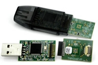
June 6, 2011 – PRNewswireTexas Instruments Incorporated (TI) (NYSE:TXN) developed a single-chip passive infrared (IR) micro electromechanical system (MEMS) temperature sensor for contactless temperature measurement in portable consumer electronics. The TMP006 integrates an on-chip MEMS thermopile sensor, signal conditioning, a 16-bit analog-to-digital-converter (ADC), local temperature sensor and voltage references on a single 1.6mm2 chip.

Click to EnlargeThe TMP006 digital temperature sensor can be used to accurately measure a smartphone, tablet, or other device’s case temperature, or to measure external temperature outside the device. It is an entirely digital product for contactless temperature measurement that is 95 percent smaller than other thermopile sensors, as it integrates the MEMS sensor and supporting analog circuitry.

The TMP006 both offers "advanced thermal management of processors," and allows app developers to "creatively tap into" the temperature measurement functionality, said Steve Anderson, SVP of TI’s High Performance Analog business. The MEMS device is primarily intended to improve user comfort by reporting device temperature, but other applications, such as those that allow users to take a room temperature, are additional benefits.

The MEMS package uses 240uA quiescent current and 1uA in shutdown mode, which TI says is a 90% drop in power consumption from competitive products. It operates in -40 to +125C with typical local sensor accuracy of +/- 0.5C and +/- 1C typical accuracy for the passive IR sensor. It includes a I2C/SMBus digital interface.

An evaluation module is available now, as is an IBIS model to verify board signal integrity requirements, along with full source code for calculating object temperature and applications notes. For more information, visit www.ti.com/tmp006-pr.

Subscribe to our MEMS Direct newsletter

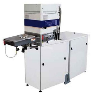
June 6, 2011 — Oxford Instruments debuted the PlasmaPro Estrelas100 deep silicon etch technology for the micro electromechanical system (MEMS) R&D and fabrication market. 

Click to EnlargePlasmaPro Estrelas100’s process flexibility enables use in R&D labs building nano and micro structures. The hardware can run Bosch and cryo etch technologies in the same chamber. The tooling meets fabrication needs of existing — accelerometers, gyroscopes — and emerging — pico projectors, energy harvesters, micro fuel cells — MEMS devices. The system is compatible with 50-200mm wafers, so devices can go to production using the same chamber hardware as development.

Increased plasma stability is said to eliminate "first wafer effect." The tool is designed to reduce polymer buildup, increasing time between mechanical cleans.

Features:

  • Mechanical and electrostatic clamp
  • Heated liners
  • Fast acting closed coupled MFCs use software originally designed for atomic layer deposition
  • Reduced chamber volume ensuring high gas conductance
  • Active spacer technology to reduce ion bombardment at the wafer surface and minimize mask undercut.

PlasmaPro Estrelas100 etch is also available on a four or six sided cluster tool. It can be used for silicon on insulator (SOI) processes.

Oxford Instruments provides high technology tools and systems for industrial and research markets with core technologies in areas such as low temperature and high magnetic field environments, Nuclear Magnetic Resonance, X-ray electron and optical based metrology, and advanced growth, deposition and etching.. The company is listed on the London Stock Exchange (OXIG).

Oxford Instruments Plasma Technology offers flexible, configurable process tools and leading-edge processes for the precise, controllable and repeatable engineering of micro- and nano-structures. Learn more at www.oxford-instruments.com

Also read: Meeting deep silicon etch challenges for silicon MEMS devices by David Lishan, principal scientist, Unaxis Semiconductors

June 3, 2011 — Japanese researchers have developed a strain sensor with oriented single-walled carbon nanotube (SWCNT) films bonded to a stretchable polymer substrate. The sensor can measure strains by detecting changes in the films’ electrical resistance.

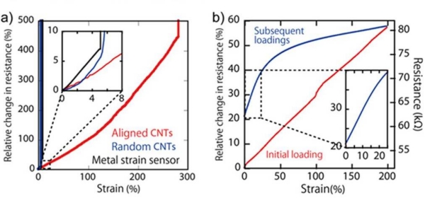
The CNT strain sensors detect strains of up to 280%, about 50x those detected by conventional metal strain sensors. It is durable for more than 10,000 repeated applications of strains less than 150% and has a 14ms strain response time. The sensor is reportedly less prone to creep than strain sensors made of a composite of an electrically conductive material and a polymer and 20x faster in creep recovery. Sensors comprising a conductive material and polymer detect strains of up to 100%, but undergo creep deformation at high strain rates. It takes more than 100 s before the deformation becomes stable and strain measurements can be made.

Click to Enlarge

Figure 1. CNT strain sensor fab method.

The Nanotube Research Center of Japan’s National Institute of Advanced Industrial Science and Technology (AIST) developed a super growth method to synthesize SWCNTs with high carbon purity (Figure 1). The high-density oriented CNT wafer is created by densification of long, vertically oriented single-walled CNT films in which the CNT films were laid horizontally on a silicon wafer. Mass fabrication of three-dimensional CNT devices was achieved by using this CNT wafer. AIST developed a technique to bond this high-density oriented CNT wafer to a soft polydimethylsiloxane (PDMS, a type of silicone rubber) substrate at any position and in any direction, making it possible to fabricate soft devices combining CNTs and a stretchable polymer substrate.

The CNT orientation is perpendicular to the direction of strains.

The team also developed a bonding technique of a soft electrode, the properties of which remain unchanged after deformation, using an adhesive made of PDMS and conductive rubber with dispersed CNTs synthesized by the super growth method. One electrode is bonded to each end of the CNT strain sensor. The electrode allows researchers to make strain sensors in which all of the components are stretchable, including the electrodes. The largest of the sensors fabricated has been 15 x 5cm.
Click to Enlarge

Figure 2. CNT strain sensor properties.

CNT sensor properties were measured at room temperature. While a conventional metal strain sensor was able to measure only small strains of up to 5%, the CNT strain sensor was able to measure strains of up to 280% (Fig. 2a). Strain sensors using random-oriented CNTs cannot measure such large strains. On the first application of the strain, the electrical resistance changed with the strain (red line, Figure 2b). On the second and subsequent applications, the electrical resistance changed differently (blue line, Fig. 2b). This curve has two linear sections with different slopes. The sensor was durable for more than 10,000 repeated applications of strains of up to 150% and showed a creep of only about 3% for the rapid application of a 100% strain. The creep became stable in 5 s.
Click to Enlarge

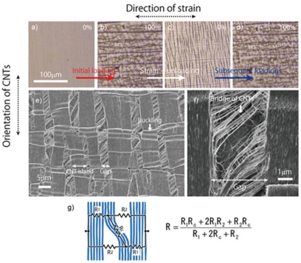
Figure 3. Stretching mechanism of the CNT strain sensor and a model of the change in electrical resistance.

The CNT sensor’s surface was observed under a scanning electron microscope (SEM) to study its mechanism. Before strain was applied, no surface irregularities were observed (Fig. 3a). On the initial application of 100% strain, buckling occurred on the CNT surface, causing cracks in the direction perpendicular to the direction of the strain (i.e. in the direction of the CNTs) (Fig. 3b and e). On the second and subsequent applications of the strain, the cracks closed when the strain was removed (Fig. 3c). When the strain was applied again, the cracks that were initially generated opened again (Fig. 3d). The opening and closing of the cracks indicates that the CNTs follow the movement of the stretchable substrate. Detailed SEMs (Fig. 3d) of the crack surface of the CNTs showed that the cracks were bridged by CNTs (Fig. 3f) and conductive paths were provided by the bridges.

Researchers introduced a CNT-bridge model (Fig. 3g) for this mechanism and calculated the change in electrical resistance. The calculated results agreed well with the measured data shown by the blue line in Fig. 2b.

Applications

The CNT strain sensor can be attached to clothing or the body to monitor knee bending and straightening, finger movement, breathing, voice production, etc., for medical or recreational purposes. One example is a data glove, which is a wearable device that could have applications from tele-surgery to immersive gaming. Conventional metal strain sensors can detect only small strains of up to 5% and therefore limit body movement.
Click to Enlarge

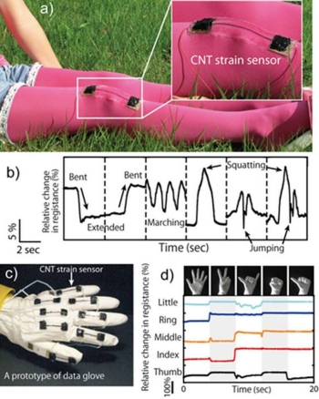
Figure 4. Monitoring knee and finger movement by using the CNT strain sensors.

In a measurement using tights to monitor knee movement (Fig. 4a), strain was applied to the sensor when the knee was bent, and the electrical resistance increased. When the knee was straightened, the strain was removed and the electrical resistance decreased. The sensor detected the change in electrical resistance with the change in knee movement (Fig. 4b). It also detected quick bending and straightening movement of the knees in jumping off the ground and knee movement in absorbing shock on landing.

CNT sensors were attached to each finger of a glove (Fig. 4c). When each finger was moved, its shape was identified by the sensor signal, demonstrating that the sensor can be applied to a data glove (Fig. 4d). As the CNT strain sensor is a highly durable device, the tights and the glove can be used repeatedly by multiple users.

Details of the study were published online in March 2011 in Nature Nanotechnology. Access the article here: http://www.nature.com/nnano/journal/v6/n5/full/nnano.2011.36.html

This study was conducted as part of the research project, "Functional Integrated CNT Flexible Nano MEMS Devices Fabricated by Self-Assembling Processes," (Research Director: Kenji Hata) in the research area, "Creation of Nanosystems with Novel Function through Process Integration" (Research Supervisor: Junichi Sone, VP, National Institute of Materials Science) of the Core Research of Evolutional Science and Technology. This project is funded by the Japan Science and Technology Agency.

The team will seek to collaborate with businesses to develop devices for commercial applications.

Team: Takeo Yamada (Senior Researcher), Super Growth CNT Team (Leader: Kenji Hata), the Nanotube Research Center (Director: Sumio Iijima) of the National Institute of Advanced Industrial Science and Technology (AIST; President: Tamotsu Nomakuchi)

Follow Small Times on Twitter.com by clicking www.twitter.com/smalltimes. Or join our Facebook group

Update August 10, 2011 – Business Wire — CMSF Corp. (OTCBB:CMSF) announced today that it has consummated the acquisition of Plures Technologies, Inc. Plures’s primary business at the present time is the ownership and operation of its Advanced MicroSensors Corporation subsidiary’s MEMS and magnetics fab in Shrewsbury, Massachusetts. Further information concerning this transaction will be set forth in a report on Form 8-K to be filed shortly by CMSF with the Securities and Exchange Commission and will be available at www.sec.gov.

June 3, 2011 – Business Wire — CMSF Corporation (OTCBB:CMSF), which has no significant operations and exists to seek a merger with an operating company, entered into such an agreement with Plures Technologies Inc. Plures, through its 95%-owned subsidiary, Advanced MicroSensors Corporation, is a semiconductor foundry developing and fabricating high-quality, high-margin micro electro-mechanical systems (MEMS) and spintronics products.

On May 23, 2011, RENN Universal Growth Investment Trust PLC and RENN Global Entrepreneurs Fund, Inc. purchased $1,500,000 and $500,000 Plures promissory notes, respectively. At the same time, CMSF agreed to a merger with Plures. When the merger occurs in the coming months, RENN Universal and RENN Global will convert their debt to equity in the combined Plures-CMSF entity, which will be called Plures Technologies Inc.

72.5% of the combined entity’s outstanding common stock will be owned by the current stockholders of Plures, 20.5% of the stock will be owned by RENN Universal, 6.8% will be owned by RENN Global and 0.2% will be owned by existing CMSF shareholders unrelated to Plures, RENN Universal or RENN Global. CMSF filed a Form 8-K on the transaction on May 25, 2011.

CMSF underwent a "long, thorough search" for an appropriate merger partner, said Stephen Crosson, chief executive officer of CMSF.

Advanced MicroSensors Corporation, Plures’ 95%-owned subsidiary, information is available at www.advancedmicrosensors.com.

RENN Universal or RENN Global information is available on www.rencapital.com.

Follow Small Times on Twitter.com by clicking www.twitter.com/smalltimes. Or join our Facebook group

June 3, 2011 — The US National Institute of Standards and Technology’s (NIST) Center for Nanoscale Science and Technology (CNST) has improved atomic force microscopy (AFM) by replacing the microscope’s optical instrumentation with a nanomechanical cantilever probe and nanophotonic interferometer on a chip.

Click to Enlarge

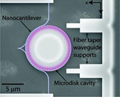
Figure. Scanning electron micrograph (SEM) of the cantilever-microdisksystem. A calculated z-component of the magnetic field is overlaid on the structure. SOURCE: NIST.

The AFM maps local tip-surface interactions by scanning a flexible cantilever probe over a surface. CNST researchers replaced the AFM’s bulky optical sensing instrumentation, which limits the tool’s sensitivity, stability, and accuracy.

The CNST researchers nano-fabricated an integrated sensor combining a nanomechanical cantilever probe with a high-sensitivity nanophotonic interferometer as a monolithic unit on a single silicon chip. The package is chip-scale, self-aligned, and stable. Fiber optic waveguides couple light with the sensor, enabling interfaces with standard optical sources and detectors.

The cantilevers are orders of magnitude smaller than those used in conventional laser-based AFMs. The detection bandwidth is increased significantly, because each smaller structures has an effective mass less than a picogram. System response time is a few hundred nanoseconds.

The probe was fabricated adjacent (>100nm gap) to a microdisk optical cavity. Light circulating within the cavity is influenced by probe tip motion. This readout technique is based on cavity optomechanics. The cavity’s high optical quality factor (Q) means that the light makes tens of thousands of trips around the inside of the cavity before leaking out of it. During this circulation, information is gathered about probe position. Small probe-cavity separation and high Q gives the device sensitivity to probe motion at less than 1 fm/√Hz, while the cavity is able to sense changes in probe position with high bandwidth.

The probe is 25µm long, 260nm thick, and 65nm wide. Probe stiffness is comparable to conventional microcantilevers, maintaining high mechanical gain. Simple probe-tip geometry changes can significantly vary the mechanics of the probe tip, which can be used to "tune" combinations of mechanical gain and bandwidth for various AFM applications.

Results were reported in Nano Letters, "Optomechanical transduction of an integrated silicon cantilever probe using a microdisk resonator," K. Srinivasan, H. Miao, M.T. Rakher, M. Davanco, and V. Aksyuk, Nano Letters 11, 791-797 (2011). Access the article here: http://pubs.acs.org/doi/abs/10.1021/nl104018r

Learn more at www.nist.gov

Follow Small Times on Twitter.com by clicking www.twitter.com/smalltimes. Or join our Facebook group
by Wenbin Ding, Yole Développement

June 2, 2011 – Demand for higher-quality sound and smaller devices will propel 23% compound average growth (CAGR) for MEMS microphones for the next five years, creating market volumes of some 2 billion units a year by 2016, for a roughly $500M business. A sign of the rate of growth: it took mic market pioneer Knowles six years to sell 1 billion units, but only 18 months more to hit the 2 billion mark in May of this year. And plenty of companies are scrambling for a piece of this growing market.

There’s lots of room for growth. MEMS microphones are still in less than 20% or so of mobile phones, but we expect that to reach 40% of phones by 2015-2016. Most voice phones still opt for lower-cost electret condenser microphones, but smart phones — with a big push from Apple’s lead example — need the higher-quality MEMS mics, and also sell for higher prices that can better cover the cost.

The applications for MEMS microphones are also growing. Notebook computers are now starting to adopt the smaller MEMS versions for the better sound, as are tablets of course, and camcorders and cameras with video options.

And demands are also getting more sophisticated, pushing the market towards the MEMS devices for multi sensor solutions for active noise cancellation, and for digital mics for less disruption from RF and EMI. Some handsets in the smart phone market are now starting to use two or more mics for noise cancellation to improve sound quality, while some notebooks use microphone array to better capture sound from users apt to not be directly in front of the microphone. Computers need digital mics to avoid interference. More sophisticated smart phones and tablets will likely increasingly adopt digital mics as well starting from about 2012, when other applications like camcorders and tablets will eventually move to multiple mics as well.

The MEMS devices continue to scale down sharply in size and in cost. By 2010 Knowles had reduced die size by 50% from 2006, for presumably twice the die per wafer, without reducing the size of the microphone diaphragm. Akustica’s latest one-chip solution from its CMOS process is only 0.70mm2. Epcos (TDK-EPC) meanwhile is using flip-chip instead of wire bonding for a thinner package.

MEMS microphone pioneer Knowles now dominates the market with more than 80% share, capitalizing on its strong background in the microphone and audio components business, its strong IP protection for its early packaging solution, its high-volume manufacturing, and a solid brand name consumer gear makers can trust — complete with the all-important used-by-Apple cachet. A crowd of challengers aims to get a piece of this growing market, both companies from the ECM microphone business, and MEMS makers. The field is littered with companies who dropped out after the first flush of interest in MEMS microphones several years ago, and with other suppliers who have yet to make significant inroads into the market — MEMS as usual have proved difficult to ramp in volume, and breaking in to the high-volume consumer phone market isn’t easy. But the current crop of both Asian ECM makers and major MEMS suppliers are likely better positioned for the challenge, as the MEMS microphone market is now well-established, and MEMS manufacturing technology is more mature.

Click to Enlarge
MEMS microphone market forecast, split by application (in millions
of units), 2010-2016. CAGR is 23%. (Source: Yole Développement)

MEMS manufacturing technology will be a focus of this year’s program at SEMICON West’s TechXPOTs: a Tuesday morning (July 12) session on "The future of MEMS: Moving from a niche to a mainstream business" (presented in cooperation with the MEMS Industry Group), and a Tuesday afternoon session on "Heterogeneous integration with MEMS and sensors." Plus exhibits and technical sessions at the Extreme Electronics TechZONE.