Tag Archives: Small Times Magazine

June 2, 2011 – Marketwire — Omron’s Micro Device Division (MDD) will release numerous micro electromechanical system (MEMS) products in the coming year, notably an absolute pressure sensor and a thermal IR sensing array.

Expanding on Omron’s piezo resistive pressure sensor technology, the company is nearing completion on a MEMS absolute pressure sensor. It is sealed on one side from atmospheric pressure and detects elevation changes at a >1 vertical meter resolution. This level of accuracy allows a person to be tracked to a particular floor of a building. Target applications include GPS navigation, portable navigation devices, weather forecasting, and vertical velocity indication. Its operating pressure is 50 to 110 kPa.

The new MEMS thermal IR sensor targets building automation and energy conservation. When positioned to scan, it can detect occupancy in a room (without movement) and measure where additional heating or cooling is required. The product comprises 8 MEMS thermal IR sensors aligned in a 1×8 array and a 4×4 array is in development. The 4×4 array would meet home appliance needs, for example, for electric stovetops.

Omron is adding new flow sensors to both sides of its current product lines: a 70 mL/min high impedance (differential pressure type flow sensor) version, and a 70-200 LPM sensor model for high flow applications.

Omron manufactures MEMS on 200mm silicon wafers, enabling costs and productivity savings by following semiconductor-method manufacturing.

Omron will demo the thermal IR sensor at Sensors Expo, June 7-8 in Rosemont, IL, at booth 307, along with existing MEMS product line expansions.

Omron Electronic Components manufactures advanced electronic components: relays, switches, connectors, MEMS flow sensors, pressure sensors, and optical components. Omron Electronic Components is the Americas subsidiary of Omron Corporation. Learn more at www.omron.com

Follow Small Times on Twitter.com by clicking www.twitter.com/smalltimes. Or join our Facebook group

June 2, 2011 – Business Wire — X-FAB Silicon Foundries released ready-to-use design IP blocks for MEMS accelerometers, as part of its MEMS foundry service offerings. The IP blocks can be used in gyroscopes and accelerometers spec’d up to 100 G-force, shortening NPI and HVM ramp.

MicroMountains Applications and HSG-IMIT (Institute for Microtechnology and Information Technology of Hahn-Schickard-Gesellschaft) helped develop the IP blocks, which can be used in MEMS capacitive accelerometer designs covering 2, 10, and 100G ranges for motion sensing in gaming systems and toys, automotive crash-detection, and more.

The fully characterized blocks run on X-FAB’s advanced open platform inertial sensor process. Development included finite element analysis (FEA) simulation on sensor elements to measure sensitivity, shock-resistance and frequency behavior. After MEMS were manufactured with X-FAB’s inertial sensor process platform, HSG-IMIT characterized the accelerometers using different rate-tables for 3-axis-simulation, temperature and vacuum; shakers; and temperature chambers.

X-FAB’s goal is to shorten accelerometer and gyroscope design times with ready-to-use IP design blocks, accelerating new product introduction (NPI) and volume ramp. One product = one process currently dominates MEMS design and manufacturing, said Iain Rutherford, business line manager for MEMS at X-FAB. Rutherford says the drop-in as-is design blocks can help push the MEMS industry to better development times on more complex MEMS devices.

X-FAB is an analog/mixed-signal foundry group manufacturing silicon wafers for analog-digital ICs (mixed-signal ICs). For more information, visit www.xfab.com

Also read:

Follow Small Times on Twitter.com by clicking www.twitter.com/smalltimes. Or join our Facebook group

June 1, 2011 — Multitest, test handler, contactor, and load board designer and manufacturer, received an order for InCarrier test equipment from a major test house in Asia, which will install an InCarrier loader/unloader, InStrip, and InMEMS module for accelerometer MEMS test.

Click to Enlarge

The InCarrier won out over standard singulated package test tools and other high-parallel test equipment. Multitest states that InCarrier overcomes strip test constraints with respect to singulation after test and lead frame design, and offers combined benefits of singulated package and parallel testers. The products also handle 2 x 2mm packages in a stable and reliable test environment, the company said in a statement.

Click to Enlarge

Multitest manufactures test equipment for semiconductors: test handlers, contactors, and ATE printed circuit boards. For more information, visit http://www.multitest.com/InCarrier.

Follow Small Times on Twitter.com by clicking www.twitter.com/smalltimes. Or join our Facebook group

June 1, 2011 – PRNewswire — Wafer bonding and lithography equipment maker EV Group (EVG) will join Taiwan’s Industrial Technology Research Institute (ITRI) to research and develop advanced manufacturing processes for next-generation micro electro mechanical system (MEMS) devices.

ITRI uses anodic, eutectic, and metal thermo compression wafer bonding in MEMS fab. EVG will help ITRI create and optimize wafer-level bonding steps. To this end, ITRI purchased an EVG510 semi-automated wafer bonding system and an EVG6200 automated mask alignment system with top-bottom alignment and bond alignment options. They will be installed in the Micro Systems Technology Center at ITRI, alongside the research group’s existing EVG mask aligners and wafer bonding tools.

ITRI plans to ramp 200mm MEMS wafer fab using the EVG510 bonder, and cited tool flexibility and process support from EVG as factors in the purchasing decision. Wafer-level aligned bonding enables MEMS fabs to process the wafer using semiconductor-style steps without damaging the mechanical features within the package. Hermetic seals created in wafer bonding also protect the device from contamination and damage during field operation.

ITRI’s partners and customers will have access to the new wafer processing technologies developed with EVG, said Tzong-Che Ho, director of ITRI’s Micro Systems Technology Center. Their goal is to bring next-generation MEMS into new and expanding applications. In Taiwan, consumer mobile communications and automotive electronics are major production areas; MEMS accelerometers, pressure sensors, gyroscopes, and other devices are increasingly used for these products.

This is a good step in EVG’s long-standing relationship with ITRI, noted Dr. Viorel Dragoi, chief scientist at EV Group, adding that the focus on MEMS process development and pilot production is a good fit for both parties.

ITRI is an international applied technology research organization focused on innovation in Taiwan.

EV Group (EVG) provides wafer-processing toolsets — wafer bonding, lithography/nanoimprint lithography (NIL), metrology equipment, photoresist coaters, cleaners and inspection systems — for semiconductor, MEMS and nanotechnology applications. More information is available at www.EVGroup.com.

Also read: Fraunhofer IMS orders Tegal equipment for MEMS fab

Follow Small Times on Twitter.com by clicking www.twitter.com/smalltimes. Or join our Facebook group

May 31, 2011 — The US Department of Energy’s Lawrence Berkeley National Lab, in partnership with the University of California at Berkeley, are working on substrates that best preserve graphene’s intrinsic nano properties. So far, the groups led by Michael Crommie and Alex Zettl, Materials Sciences Division, Berkeley Lab and UC-Berkeley physics professors researched graphene’s interaction with a boron nitride substrate.
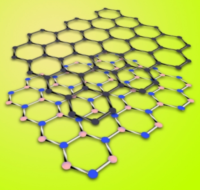
Click to Enlarge

Figure 1. Graphene (top layer) is a hexagonal "chicken wire" arrangement of carbon atoms. Hexagonal boron nitride is a similar arrangement of boron and nitrogen atoms; its lattice constant is just 1.7% larger than graphene’s. 

Graphene’s intrinsic properties — very high electron mobility, very low resistivity — are best studied on suspended graphene, notes Régis Decker, a former postdoctoral fellow in the Crommie group, now at the University of Hamburg, Germany, and lead author of the results published in Nano Letters. Any substrate will affect graphene’s properties. Unfortunately, suspended graphene is unstable under scanning probe microscopy (SPM). The next best thing is to use a substrate that minimally changes graphene’s properties, while lending enough structure to prevent vibration during scans. A graphene substrate should have a large electronic band gap and no dangling bonds if it is to mimic "pure" graphene, said Decker. Suspended graphene is also very flat, which is a desirable substrate property.

A group based at Columbia University reported, in October 2010, that graphene supported on a boron nitride (BN) substrate had dramatically better electron mobility than graphene mounted on the most common semiconductor substrate, silicon dioxide (SiO2). However, the team’s macroscopic measurements couldn’t answer some fundamental research questions, said Yang Wang, co-lead author of the Nano Letters report. The Crommie and Zettl groups compared BN and SiO2 to find out why boron nitride was so inobtrusive. Scanning tunneling microscopy (STM) helped the researchers build up a picture of the substrate’s topography and measure its local electronic states.

In boron nitride’s hexagonal structure (h-BN), alternating nitrogen and boron atoms closely mimic the way carbon atoms are arranged in graphene. Boron and nitrogen atoms in BN compounds are paired equally, and together their valence electrons (three and five, respectively) equal those of a pair of carbon atoms (four each). Although the h-BN lattice is some 1.7% larger than graphene’s, the two honeycombs laid one on the other can be aligned much more closely than graphene and silicon dioxide. Unlike graphene, which normally has no band gap, h-BN has a wide band gap, due to the alternating boron and nitrogen atoms in its lattice. This could lead to graphene with a bandgap, which, while altering graphene’s properties, could lead to interesting applications.
Click to Enlarge

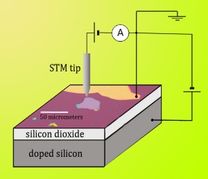
Figure 2. The Berkeley researchers deposited BN flakes on a layer of silicon dioxide, grown on a layer of doped silicon. The doped silicon was used as a gate electrode for doping the graphene during STM. Graphene was applied to both the boron nitride flakes (under the STM tip) and the bare silicon dioxide; the graphene (dark and light purple) was grounded by an electrode of gold/titanium (gold). The STM could scan across both substrate systems.

To create graphene/BN devices, Zettl’s group reduced boron nitride crystals to tiny flakes by exfoliating them between strips of Scotch Tape, then deposited the flakes onto a silicon dioxide layer grown on a layer of doped silicon. This method allowed the researchers to dope the graphene layer during STM.

The Crommie group’s Qiong Wu created graphene via chemical vapor deposition (CVD) on copper, which allows the carbon atoms to self-assemble into an atom-thick honeycomb lattice. The graphene sheets were then transferred from the copper to soft plastic and pressed onto the boron nitride flakes. The assembly was annealed at high heat. A layer of titanium gold electrode grounded the graphene.

Three graphene/BN systems were made for direct STM comparisons with graphene on silicon dioxide. Researchers measured topography and local charge concentrations at various doping levels determined by the silicon-layer gate electrode.

Boron nitride vs silicon dioxide

Atmospheric impurities in substrates alter graphene properties, shortening the electrons’ mean free path by creating "puddles." Charge puddles were notably absent from the BN substrate samples, said Victor Brar of the Crommie group. Practical graphene-based devices on BN substrates could be manufactured without the vacuum atmosphere that typically protects against water, air, and other impurities.
Click to Enlarge

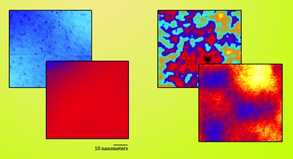
Figure 3. Measuring graphene on a boron nitride substrate (left), graphene on silicon dioxide (right). The STM mapped both topography (back) and local charge densities (front).

Dangling bonds (valence electron available for bonding with another atom) can mess with graphene properties as well. SiO2 has a high concentration of dangling bonds; boron nitride has none.

Topographically, graphene on boron nitride is much less rough than graphene on silicon, with height differences on the scanned surfaces reaching only around 40 picometers (trillionths of a meter). Height differences with the silicon dioxide substrate were up to 30 times greater.

Electronically, variations in charge density were reduced dramatically in the BN substrate, nearly unvarying.

The Crommie group investigated how electronic properties might vary according to the orientation of the graphene sheet on the boron nitride substrate. The two, not-quite-commensurate lattices betrayed their alignment by exhibiting changing moiré patterns with different orientations. Wang reports seeing many different alignments, including alignments that were "almost perfect," but no band gap.

The work recently appeared in Nano Letters: "Local electronic properties of graphene on a BN substrate via scanning tunneling microscopy," Régis Decker, Yang Wang, Victor W. Brar, William Regan, Hsin-Zon Tsai, Qiong Wu, William Gannett, Alex Zettl, and Michael F. Crommie,  http://pubs.acs.org/doi/abs/10.1021/nl2005115.

After the Crommie and Zettl groups submitted their paper, related work by Xue et al appeared in Nature Materials, April 2011, available online at http://www.nature.com/nmat/journal/v10/n4/abs/nmat2968.html.

Visit Berkeley Lab’s website at http://www.lbl.gov/

Follow Small Times on Twitter.com by clicking www.twitter.com/smalltimes. Or join our Facebook group

May 31, 2011 Micro-cantilevers can measure lipid bilayers interactions with surfactants with a new level of sensitivity, say Rice University researcher Sibani Lisa Biswal, assistant professor in chemical and biomolecular engineering, and Kai-Wei Liu, a graduate student in Biswal’s lab.

Lipid bilayer membranes surround living cells and work with specific membrane proteins as "gate keepers": letting ions, proteins and other essential molecules into the cell. Individual lipid molecules in the bilayer have a hydrophilic head and two hydrophobic tails. They aggregate into two-layered sheets, with the heads pointed out and the hydrophobic tails pointed inward.

Liu and Biswal have previously worked on attaching lipid bilayers to microcantilevers. A protective coating on the thin gold layer makes the top of the cantilever inert, so the membranes attach themselves to and spread out over the silicon dioxide bottom. The membrane’s interaction with the cantilever affects surface tension, bending the cantilever enough to be measured by a laser sensor with nanometer resolution.

In their current work, the researchers introduced varying concentrations of lysolipids to the supported lipid bilayers. Lysolipid compounds lower liquids’ surface tension, and have a hydrophilic head but only one hydrophobic tail. They are surfactants that can be used in detergents, among other applications. Based on the experimental results, measured by the micro-cantilevers, detergents could be fine tuned to better destroy stains.

"The cantilever naturally wants to bend with whatever force the membrane puts on it," Biswal said. Cantilever structures are the simplest micro-electromechanical systems (MEMS) that can be easily micromachined and mass-produced.*

In low concentrations, lysolipid molecules wedge themselves into the bilayer, while their hydrophobic tails join up to the membrane’s hydrophobic inner ring; changing the surface tension on the cantilever, Liu and Biswal found.

In high concentrations, lysolipid monomers form micelles, rings of molecules that interact with the membranes and disrupt the hydrophobic interactions that keep them together. Depending on their strength (determined by the chemical makeup of their hydrophobic tails), the micelles can either weaken the membranes by pulling lipid molecules away or destroy the membranes completely.

Biswal sees other potential for the technique. "We’re interested in using this as a general platform for looking at small molecules," she said.

Liu is studying how hepatitis C peptides behave in the presence of a microcantilever-mounted membrane. "This could be a way to probe how viruses are able to enter cell membranes or disrupt proteins on their surfaces," she said.

Biswal suggested that carbon-60 atoms — buckyballs — might also be a good subject, because they are naturally hydrophobic. Research on buckyballs could advanced understanding of nanomaterial/cell interaction.

Results were reported online in the American Chemical Society journal Analytical Chemistry. Access the article here: http://pubs.acs.org/doi/abs/10.1021/ac200401n

The Robert A. Welch Foundation funded the research.

Learn more at www.rice.edu

Follow Small Times on Twitter.com by clicking www.twitter.com/smalltimes. Or join our Facebook group
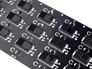
May 30, 2011 – NIST Tech Beat — As smartphones usher in a host of new high-volume MEMS applications, semiconductor and electronics roadmaps are paying serious attention to the manufacturing and costs gaps in MEMS production. NIST’s Michael Gaitan and the MEMS Industry Group are helping shape iNEMI, ITRS roadmaps with MEMS in the spotlight.

The smartphone is becoming mobile electronics king, but the army supporting it is lead by micro electro mechanical systems (MEMS). MEMS create mobile speakers, projectors, gyroscopes and other devices integrated onto mobile computing platforms, notes the US National Institute of Science and Technology (NIST).

NIST reports that MEMS revenues (about $7 billion in 2010) largely come from high-volume industrial and automotive sectors: accelerometers (for airbags) and other sensors for the automotive industry, ink-jet printer head components, display and hard-disk drive technologies. MEMS devices were once seen as distantly related to computer chips and consumer electronics, said Michael Gaitan, Enabling Devices Group leader, NIST, adding that mobile computing devices like smart phones and tablets are propelling so-called ‘New MEMS’ onto the main stage in semiconductor/electronics industries with their "rapid growth."
 
The International Electronics Manufacturing Initiative (iNEMI) has produced technology roadmaps for the electronics industries since 1994. iNEMI’s recently issued nearly 2000-page technology roadmap includes a chapter, drafted by the MEMS Technology Working Group (Gaitan chaired the group), on MEMS technology evolution. Special attention went toward the technical challenges to achieving MEMS manufacturing capabilities that will be required over the next 10 years.

Challenges and gaps exist in:

  • device and reliability testing,
  • wafer-level testing,
  • modeling and simulation tools to support MEMS design, 
  • assembly and packaging standardization.

Gaitan, who is currently on assignment to the NIST Technology Innovation Program, sees cooperation as key. Test costs comprise up to half a MEMS’ manufacturing costs, he points out. Gaitan chairs the new MEMS Technology Working Group, which will contribute to the next version of the International Technology Roadmap for Semiconductors (ITRS). The working group will concentrate on microphones, accelerometers, gyroscopes, etc., in next-gen smart phones, as well as emerging MEMS for mobile opportunities. Projecting 15 years out, the working group is assessing device performance needs, design and simulation tools, packaging and integration, and testing. Conclusions will be included in the 2011 ITRS, to be issued later this year.

The MEMS Industry Group, a trade association focused on advancing MEMS across global markets, has contributed to both roadmapping activities.

NIST’s participation in the iNEMI and ITRS efforts helps to guide its laboratory programs aimed at developing the measurement capabilities that industry will require to make current and next-generation technologies.

The National Institute of Standards and Technology (NIST) is an agency of the U.S. Department of Commerce.Learn more at www.nist.gov

Follow Small Times on Twitter.com by clicking www.twitter.com/smalltimes. Or join our Facebook group
Click to Enlargeby Jan Provoost, science editor, imec

May 27, 2011 – Closing the technical sessions of this year’s ITF, Harmke de Groot, imec program director for ultralow-power technologies, discussed automated body monitoring, and how it could impact future healthcare.

The vision she painted is one of unobtrusive, comfortable sensors that are worn on the body — possibly hidden into clothing, attached to the body as intelligent patches, or even, in the extreme case, implanted. Sensors that measure body parameters and send them wirelessly to a base station and from there on to the hospital.

People suffering from chronic diseases, or elderly people that need watching, could be monitored from their homes. The result would be a win-win: for the healthcare system, automated home monitoring would be cheaper and would free many resources; and for patients, they could be monitored without leaving their homes, permanently and comfortably.

To make this vision come true technically, most of the raw building blocks are available, e.g. sensors, wireless radios, etc. The main exercise now is to integrate these in a package that really delivers on the promise.

One issue, for example, is energy use and autonomy. To make home monitoring really attractive, you’d need sensors that can work for weeks without needing to be replaced or batteries recharged. That is no easy requirement, requiring orders-of-magnitude gain in energy efficiency compared to commercially available electronics. Over the past few years, imec has done a lot of R&D in this area. Recently, it unveiled a new ultralow-power radio component, dedicated for use in body sensors, and a new versatile ultralow-power biomedical signal processor, CoolFlux, made in collaboration with NXP. With these components, and through careful co-design and co-optimization of all the components, imec made monitoring nodes that sense, compute, and send for over a week on a single small battery.

To illustrate the possibilities, imec integrated its components in prototype applications, for example a full-ECG monitor in the form of a lightweight necklace. The ECG remains functional even when the wearer moves around, sending a full ECG reading to a base station that may be up to 10 meters away from the wearer.

Click to Enlarge
Demonstrator ECG necklace with ultralow-
power wireless radio. (Source: imec)

May 27, 2011 — G24 Innovations (G24i), dye sensitized solar cell technology (DSSC) provider, and Texas Instruments (TI, NY:TXN) will combine G24i’s solar cell technology with TI’s nano-powered energy converter under a new strategic development agreement. Their aim is autonomous self-powering devices for OEMs, including computer mice, keyboards, intelligent sensors, and more.

G24i’s Gen-3 DSSC technology is an efficient indoor energy harvesting system. Combined with TI’s technology, it promises devices will have better energy efficiency, and standby power for industrial and home automation uses, said Richard Costello, chief operating officer at G24i. The increased device energy efficiency and lower carbon footprint is possible because of the combined light energy and energy harvesting capabilities, added Martin Carpenter, business development manager at Texas Instruments.

Also read: G24, Chinese institutes to push dye-solar tech and check out our Energy Storage Trends blog.

G24 Innovations (G24i) is a global manufacturer of next generation Dye-Sensitized Solar Cells (DSC). Learn more at www.g24i.com.

Texas Instruments manufactures semiconductors. Learn more at www.ti.com.

Follow Small Times on Twitter.com by clicking www.twitter.com/smalltimes. Or join our Facebook group

May 27, 2011 — Based on COMSOL Multiphysics simulation software, the new COMSOL Inc. Microfluidics Module enables users to study microfluidic devices and rarefied gas flows. The module is designed for microfluidics and vacuum researchers and engineers.

The Microfluidics Module can be used with lab-on-chip devices, inkjet technology, digital microfluidics, electrokinetic and magnetokinetic devices, biosensors, and vacuum system designs. Tutorials and relevant models can be used for instruction or a starting point for experiments (Capillary Rise, Jet Instability, Drug Delivery System, Electrokinetic Valve, Electroosmotic Mixer, Electrowetting Lens, Lamella Mixer, Star Chip, Viscous Catenary, Vacuum Capillary, and Ion Implanter). Read more about ion implant here.

Microfluidics device simulation requires the researcher to incorporate multiple physical effects, noted Dr. James Ransley, who developed the Microfluidics Module with COMSOL. The Microfluidics Module’s toolset handles single- and multi-phase flows, transport and chemical reactions, flow in porous media, and rarefied flows. One user interface allows users to couple physics phenomena with thermal and electromagnetic effects, he added.

Interfaces for single-phase flow simulate compressible gas flows at low pressures, non-Newtonian flows (such as blood flow), and laminar and creeping flows that typically occur in lab-on-a-chip systems, and similar applications.

The module’s modeling interfaces for executing two-phase flow simulations use the level set, phase field, and moving mesh methods. It accounts for fluid-interface effects such as capillary forces, surface tension forces, and Marangoni effects.

Electrokinetic and magnetohydrodynamic models can be set up to simulate electrophoresis, magnetophoresis, electroosmosis, dielectrophoresis, and electrowetting effects. These suit research into existing and emerging passive electronic display technologies.

Chemical diffusion for multiple dilute species allows simulation of processes occurring in lab-on-chip devices and biosensors.

The Microfluidics Module’s free molecular flow interface uses the fast angular coefficient method and enables imulations where the molecular mean free path is much longer than the geometric dimensions. Vacuum system designers can use the tool in combination with COMSOL’s LiveLink interfaces for industry-standard CAD packages, running quick parametric studies of chamber geometries and pump configurations.

COMSOL Multiphysics is a software environment for the modeling and simulation of any physics-based system. Optional modules add discipline-specific tools for mechanical, fluid, electromagnetics,  and chemical simulations, as well as CAD interoperability. Learn more at www.comsol.com.

Follow Small Times on Twitter.com by clicking www.twitter.com/smalltimes. Or join our Facebook group