Tag Archives: Small Times Magazine

May 10, 2011 — For the MEMS industry in general and for Japan’s MEMS sector in particular, the damage from the March 11 earthquake and tsunami was not as severe as initially feared due to a fortuitous accident of geography.

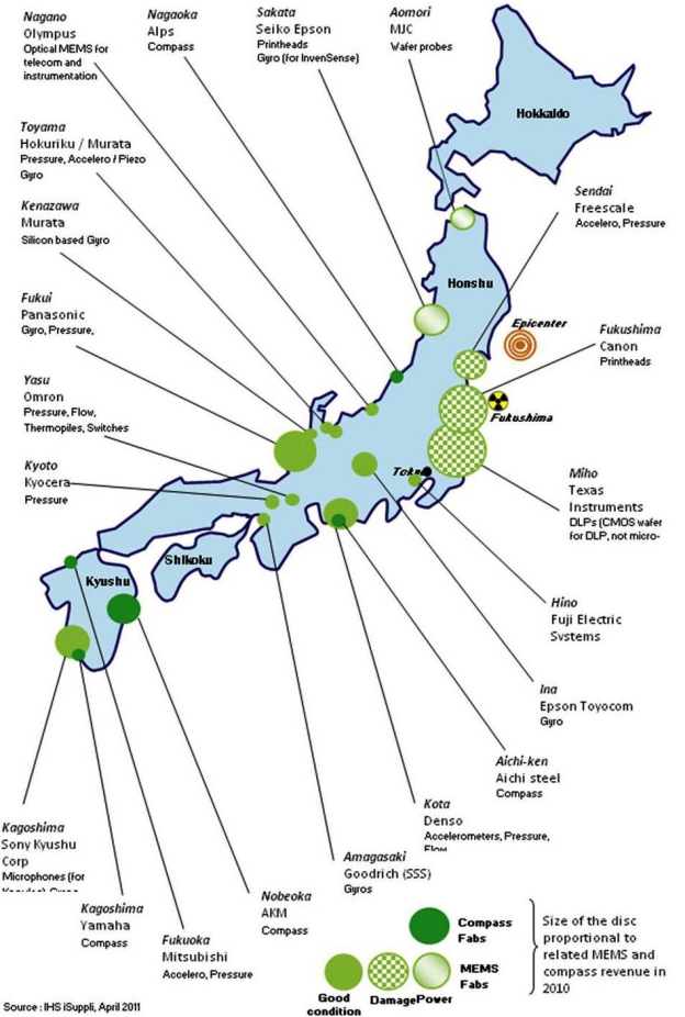
Most MEMS fabs and foundries are located in southern Honshu, away from the disaster-devastated northern section of Japan, notes Jérémie Bouchaud, director and principal analyst for MEMS at IHS. MEMS and compass suppliers had been employing multiple fabrication plants for manufacturing before the March 11 earthquake and tsunami occurred, reducing the impact of supply disruptions caused by damage to a specific factory.
Click to Enlarge


"To date, the supply of MEMS sensors and actuators remains only slightly affected by the Japan catastrophe," said Jérémie Bouchaud, director and principal analyst for MEMS at IHS. "In fact, the main effect of the earthquake on the world MEMS industry is on the demand side, not on supply. Manufacturers of finished electronic products have been more severely impacted than the component suppliers."

9 of the top 50 MEMS manufacturers worldwide are Japanese companies (Canon, Panasonic, Epson and Denso all rank among the Top 20 in the global MEMS space), and Japan is a strong manufacturing base for MEMS companies headquartered in western countries. Japanese companies sold some $1.38 billion worth of MEMS in 2010, representing 21.3% of the global market.

Approximately 32.5% of MEMS sensors and actuators in value were processed — partly or entirely — in Japanese facilities in 2010, corresponding to revenues from both Japanese MEMS companies and from foreign companies that have their MEMS processed in Japan. Western companies with MEMS facilities in Japan include Freescale Semiconductor, Knowles Electronics, Goodrich Corp. and Texas Instruments Inc. for the complementary metal-oxide semiconductor (CMOS) circuitry of its digital light processing (DLP) chipsets.

Japan makes nearly all of the world’s digital compasses. Compasses rapidly are becoming a standard feature in tablets and cell phones equipped with global positioning system (GPS) functionality. Worldwide shipments of digital compasses reached 263 million units in 2010, up 354% from 58 million the earlier year, with shipments expected to rocket to 1.28 billion units by 2015, IHS iSuppli research indicates. Four Japanese firms — AKM Semiconductor, Yamaha Corp., Aichi Steel and Alps Electric — accounted for 97% of the global supply of digital compasses.

Only three of the 22 most important MEMS and compass fabrication plants in Japan suffered direct damage, IHS iSuppli research shows, although 19 fabs potentially could be affected by the same logistical and power issues impacting all Japanese industries in the calamity’s aftermath. The three damaged facilities belonged to Freescale, Canon Corp. and Texas Instruments, shown in the attached figure pinpointing the location of MEMS and digital compass fabrication facilities throughout Japan.

  • According to Freescale, the company has decided to close its 150mm fab in Sendai, near the quake’s epicenter, and focus efforts on accelerating the transfer of MEMS production to its 200mm Oak III fab in Texas. Freescale was lucky in that the Sendai fab had been scheduled for shutdown by the end of 2011, and the company already had built buffer inventories. Had it not made this decision in 2009, Freescale and its customers would have been severely hurt, IHS believes.
  • For Canon, which makes printers and MEMS print heads in the city of Fukushima, site of the nuclear meltdown, production was halted after significant damage to the company’s plant. However, Canon managed to repair the damage very quickly, with the plant completely operational again by the first week of April. As a result, the impact of the disaster on Canon’s MEMS revenue for 2011 is expected to be very modest, IHS iSuppli data indicate.
  • For its part, Texas Instruments’ Miho fab northeast of Tokyo has undergone the repair of various infrastructure systems for water, gases and chemicals. Full production will resume by the middle of July, with full shipment capacity to commence before September, the company said. Prior to the catastrophe, Texas Instruments already was using multiple fabs for the fabrication of CMOS wafers for DLP MEMS chips, and the company is in a fortunate position to rapidly increase production at its other fabs to compensate for the disruption at Miho.

To learn more about this topic, see the new IHS iSuppli report "The Japanese Disaster and Its Impact on the MEMS and Compass Industry" http://www.isuppli.com/MEMS-and-Sensors/Pages/The-Japanese-Disaster-and-Its-Impact-on-the-MEMS-and-Compass-Industry.aspx?PRX

Follow Small Times on Twitter.com by clicking www.twitter.com/smalltimes. Or join our Facebook group

Peter Singer, editor-in-chief, Small Times and ElectroIQ.com

May 9, 2011 — ElectroIQ’s chief editor Peter Singer recently toured the Center for Advanced Materials Processing (CAMP) at Clarkson University in Potsdam, NY. The Center is largely focused on the synthesis and processing of advanced materials. The following video interviews with researchers and professors cover nanotechnology in aerospace technology, cleanrooms, illumination, and energy technologies, among other topics.

A tour of Clarkson U’s research labs

Ratneshwar Jha, Clarkson University, shows us his laboratory at the school, describing the research they perform. Professor Jha explained how, in the Smart Structures laboratory, they are using a scanning laser vibrometer and a synthetic jet actuator — which has a very small (10-30mm) piezoelectric membrane — to develop new techniques for active flow control. "That kind of active flow control can energize flow, reduce drag and increase lift which could be really useful for airplanes," he said.

Other work involves carbon fiber plates. "We are looking into finding defects in that plate based on the propagation of lamb waves (detected by laser vibrometer)," he said. 

Biotechnology lab tour

Professor Evgeny Katz shows us the bioelectronics and biotechnology lab at Clarkson University, where they research biocomputing (similar to biosensing) and other fields using bio-chemical reactions. Professor Katz explained that in the biotechnology lab, they are working on biocomputing: "We are trying to process by chemical means different biochemical signals. It’s similar to biosensing but we are processing multiple signals to make logical conclusions, not using computers but biochemical reactions." This could be very useful for monitoring health conditions.

One research project presently underway, funded by the DoD, has a goal of giving wounded soldiers immediate assistance. "It might be possible in the near future to analyze biomedical conditions with our system and give a signal to a chemical actuator to process and inject the appropriate drug," he said.


Particle engineering for better medicine

Richard Partch, a senior professor at Clarkson University, discusses the breadth of chemistry, and goes in-depth of medicinal apps. Partch talked about the medicinal chemistry aspect of their work, which is focused on making micro-emulsions that can bind to commonly overdosed drugs so that can be quickly inactivated. Future antidotes for overdoses are in the works. Other work includes attaching DNA to particles for security applications.


View videos from Clarkson University on semiconductor technologies

View Clarkson videos on photovoltaics technologies


Clarkson U research on particle transport

Goodarz Ahmadi, Dean of Engineering at Clarkson University (with the university for 30 years, Ahmadi has served as a dean for the past 5), discusses his research interests: particle transport in various environments, including particulate contamination in semiconductor manufacturing.

Ahmadi says: "We look at how particles are transported in various environments, such as in a room or in human respiratory systems. Also, we look a lot of industrial applications. I’ve done work with IBM, Xerox, Kodak, Corning and other companies, looking at issues that they had with particulate transport in various applications from copier machines to contamination of chip manufacturing systems. We’ve also done work for the NSF, NASA and the DoE related to energy issues."

CMP work at Clarkson U

S.V. Babu (also with the school for 30 years) discusses particle synthesis and chemical mechanical planarization (CMP) research taking place at Clarkson University. Babu has studied CMP for 15 years.

Babu says: "We have leveraged the expertise of CAMP in colloidal science and thin film processing. A lot of our students who have graduated are now running the CMP operations at IBM, Intel and Micron."

Bio-compatible ultra-bright fluorescent nanoparticle research

Igor Sokolov, Physics and Chemistry Professor at Clarkson University, shares info on ultra-bright nanoparticles that are substantially brighter than quantum dots.

Acoustics in engineering materials

Cetin Cetinkaya, Professor of mechanical engineering at Clarkson University, researches acoustics. Acoustic waves can be used to characterize drug function and effectiveness. Semiconductor nanoparticle removal can also be accomplished with acoustic waves.

Airborne particles and industry

Suresh Dhaniyala, Clarkson University, discusses airborne particles. These can be contaminants in the semiconductor fab. He shows us Clarkson U’s instruments to study particles.


Nanostructured thin films for energy apps, biomed

Sitaraman Krishnan, assistant professor in the chemical engineering department at Clarkson University, discusses his research on nanostructured thin films for bio/life sciences and energy (solar cells and fuel cells).

The visit was arranged by Tim Dunn, VP, marketing and business development, Mohawk Valley EDGE and the Marcy NanoCenter in Rome, NY and Mike Novakowski, director of business development, CenterState Corporation for Economic Opportunity, NY’s Creative Core in Syracuse, NY.  This was part of a tour of various prestigious universities in upstate New York (including Cornell University, Syracuse University and Binghamton University, as well the Syracuse Center of Excellence), with an eye on how well they could help businesses that decide to locate there.

Subscribe to Solid State Technology/Advanced Packaging.

Follow Solid State Technology on Twitter.com via editors Pete Singer, twitter.com/PetesTweetsPW and Debra Vogler, twitter.com/dvogler_PV_semi.

Or join our Facebook group

May 9, 2011 — Pyrograf Products Inc.’s quality management system has been ISO 9001:2008 certified. In the growing field of carbon nanotube (CNT) manufacturers, ISO certification provides essential customer confidence and company credibility, states Pyrograf Products.

Pyrograf Products developed quality control methodologies for the commercial scale production of stacked-cup carbon nanotubes (CNT), also known as carbon nanofiber. The company recently consolidated 15 years of carbon nanotube quality control experience and expertise into a quality management system and was granted ISO 9001:2008 certification.

ISO 9001 provides a suite of proven business and quality management techniques to efficiently and effectively operate a successful business. Pyrograf Products developed its quality management system according to ISO standards over a one-year period and then underwent a thorough analysis of its policies and procedures conducted by Eagle Registrations Inc. Eagle, based in the Dayton, OH area, is an ANSI-ASQ National Accreditation Board (ANAB) accredited registrar.

Certification through Eagle to ISO 9001:2008 ensures consistent quality and continual improvement of products to provide an added sense of confidence in Pyrograf-III carbon nanofiber, says Pyrograf. "ISO certification provides an internationally recognized means for us to communicate Pyrograf’s commitment to quality and continuous improvement to our customers," said David Burton, GM.

Pyrograf-III is a patented, highly graphitic, low-cost stacked-cup carbon nanotube with properties approaching the theoretical values of graphite in almost every performance characteristic. Pyrograf-III stacked-cup carbon nanotubes are a highly pure product with over 99.9% fibrous material and very low metal concentrations. Pyrograf Products produces stacked-cup carbon nanotubes with an annual capacity of 50,000 lbs per year. Pyrograf-III stacked-cup carbon nanotubes are currently being used worldwide to provide mechanical, electrical, and thermal advantages in polymeric composites.

Also read: CNT, graphene, and other nanocarbon production lags capacity 

Pyrograf Products, Inc., an affiliate of Applied Sciences, Inc., was incorporated in 1996 to manufacture carbon nanofiber in commercial volumes under the trade name Pyrograf-III. Applied Sciences, Inc. (ASI) has developed a national reputation as a research organization specializing in advanced materials and their applications. Learn more at http://pyrografproducts.com

Follow Small Times on Twitter.com by clicking www.twitter.com/smalltimes. Or join our Facebook group
May 9, 2011The Dolomite Centre Ltd, designer and manufacturer of microfluidic devices, signed a collaboration agreement with Sphere Fluidics, a leading company in commercializing picodroplet technology that performs thousands of simultaneous analyses on single cells and small populations of molecules.

Sphere Fluidics is commercializing new lab-on-a-chip and picodroplet technology developed at Cambridge University by company founders Professor Chris Abell and Professor Wilhelm Huck. Sphere Fluidics offers expertise in miniaturized discovery systems and services based on microfluidics and picodroplets.

Focusing on storing and retrieving individual picodroplets containing a unique sample, Sphere Fluidics’ technology benefits rapid antibody discovery, identification of novel algal strains, generation of new biocatalysts, etc.

The agreement between Sphere Fluidics and Dolomite establishes core areas where the two companies will collaborate:

  • Dolomite will become the exclusive worldwide distributor for Sphere Fluidics’ standard products, including a range of PDMS picodroplet handling chips and surfactants;
  • Dolomite will develop and sell new products in picodroplet technology, based on Sphere Fluidics’ expertise.

Dolomite expects to add further functionality, such as droplet merging, via the collaboration. Sphere Fluidics expects the cooperation to bring its technologies to market faster.

"Microdroplets are a fascinating and fast growing area of research, especially useful where tests need to be conducted on only a few nanolitres of sample containing, for example, cells or DNA," commented Dr. Andrew Lovatt, CEO of Dolomite.

Sphere Fluidics is commercializing new lab-on-a-chip and picodroplet technology from Cambridge University that can perform thousands of simultaneous reactions on single cells and small populations of molecules contained within aqueous droplets, fractions of a millimetre in size. For more information please visit www.spherefluidics.com

A Microfluidic Application Centre, Dolomite focused on working with customers to turn their concepts for microfluidic applications into reality. For more information please visit www.dolomite-microfluidics.com


Follow Small Times on Twitter.com by clicking www.twitter.com/smalltimes. Or join our Facebook group

May 6, 2011 – BUSINESS WIRE — Optics Balzers, optical coating partner, is offering a portfolio of patterning technologies for producing high-grade optical components. Depending on the application, patterning techniques such as photolithography, laser ablation, or masked coatings are available.

Beside the core business of coating optical thin film components, Optics Balzers also offers additional processing steps such as patterning of optical components. Most patterning solutions are used in conjunction with the sputter technology developed by Optics Balzers.

Photolithography capabilities such as wet etching, reactive ion etching, and lift-off techniques allow the manufacture of high-precision patterned coatings and gratings in the submicron range. Photolithographic techniques are specifically applied in the production of lids for micro electromechanical systems (MEMS) elements and CCD/CMOS image sensors. This method enables pattern sizes smaller than 10 microns to be produced.

Laser ablation offers novel options for patterning optical filter coatings. Through the application of customized processes high-precision patterns can be generated on the coated components. Laser ablation provides flexibility in producing customized shapes and patterns as well as very short processing times. It is possible to manufacture patterned filters down to a minimum pattern size of 100 microns by means of this technology.

Metal masks fixed to the substrates generate patterns during the coating process. The achievable pattern size and shape that this technology allows is limited, with the minimum size being around 200 microns. The advantage of the masked coating technique is that patterning can be applied with almost any coating process and material, including processes requiring high temperatures.

Together with its subsidiary in Jena, Optics Balzers supplies optical coatings and components. More information is available at www.opticsbalzers.com.

May 6, 2011 – PRNewswire — STMicroelectronics (NYSE: STM), micro electromechanical systems (MEMS) supplier, launched a complete hardware solution for advanced sensing applications with 10 degrees of freedom (DoF). A set of 3 thin, high-performance MEMS sensors provides accurate and comprehensive information on linear, angular, and magnetic motion together with altitude readings, enabling enhanced navigation and smarter user interface in mobile phones and other portable consumer devices.

An emerging new class of mobile consumer applications, such as location-based services and pedestrian dead-reckoning for indoor and multi-floor navigation, require rather complex sensing capabilities. By using three ST MEMS sensors — a geo-magnetic module, a gyroscope, and a pressure sensor — a consumer device can have a complete indication of its linear acceleration, angular velocity, earth gravity, heading and altitude. With this information, mobile users will be able to identify their direction and precise location in all three dimensions everywhere they go, including in places with no or low GPS signal: inside buildings in urban canyons, or in mountainous and forested terrain.

Facilitating the fusion of complex motion-sensor data in smart consumer devices, ST has also recently introduced an advanced filtering and predictive software engine, which integrates the outputs from 3-axis accelerometers, gyroscopes and magnetic sensors. Fusing these sensors’ data through sophisticated algorithms, the iNEMO Engine delivers more accurate and reliable sensor performance.

"Multi-sensor capabilities enhance the mobile user experience with previously unseen realism and accuracy in next-generation motion- and location-based applications," said Benedetto Vigna, group VP and GM of ST’s MEMS, Sensors and High Performance Analog Division.

Designed and produced using the same micromachining technology process that the company applies to its more than 1.2 billion sensors, ST’s MEMS chips boast ultra-small size and minimized current consumption coupled with superior accuracy and reliability. The three-chip 10-DoF sensor solution comprises the following components:

  • The LSM303DLHC geo-magnetic module integrates high-resolution, three-axis sensing of linear and magnetic motion in a 3 x 5 x 1mm package, with operating current consumption as low as 110 microamps. The device delivers extremely accurate output across full-scale extended ranges up to +16g (linear acceleration) and +8 Gauss (magnetic field), with excellent stability over time and temperature.  In addition to that, it comes with a host of advanced features, including 4D/6D orientation detection and two programmable interrupt signals that enable immediate notification of motion detection, free fall and other conditions.
  • Housed inside a 4 x 4 x 1mm package, the L3G4200D 3-axis digital gyroscope provides state-of–the-art performance in terms of output accuracy and stability over temperature and time. The device couples a 16-bit data output with a wide set of user-programmable full-scale ranges from +250dps up to +2000dps. An embedded FIFO (first-in first-out) memory block removes the need for continuous communication of between the sensor and the host processor, decreasing dramatically the overall power consumption.
  • ST’s soon-to-be-announced silicon pressure sensor uses an innovative technology to provide extremely high resolution measurements of pressure — and therefore also of altitude — in a 3 x 3 x 1mm package. The device has an operating pressure range of 260-1260 millibars, corresponding to the atmospheric pressures between -700 and +10000m relative to sea level, and can detect height variations as small as 0.3m.

ST’s 10-DoF sensor solution is now available for evaluation, with mass production scheduled for the end of Q3 2011.

STMicroelectronics creates innovative semiconductor solutions for multimedia convergence and power applications. For further information on ST’s MEMS solutions, go to www.st.com/mems.

Follow Small Times on Twitter.com by clicking www.twitter.com/smalltimes. Or join our Facebook group
May 6, 2011 — Evident Technologies Corporation and Samsung Electronics Co. Ltd entered into a comprehensive patent licensing and purchasing agreement for Evident’s quantum dot LED technology. This agreement grants Samsung worldwide access to Evident’s patent portfolio for all products related to quantum dot LEDs from manufacture of the quantum dot nanomaterials to final LED production.

"We are excited that Samsung, the leader in consumer electronics, has licensed our quantum dot technology," said Dr. Clint Ballinger, CEO of Evident Technologies. "We already enjoy a terrific working relationship and look forward to the future of this technology."

Quantum dots are nanometer-sized semiconductor crystals that have great commercial promise in electronic applications from solar energy conversion to thermoelectrics to LEDs. Evident commercialized quantum dot LEDs with products launched in 2007.

Evident Technologies is a nanotechnology company specializing in the creation of semiconductor quantum dots. Learn more at http://www.evidenttech.com/.

May 5, 2011Crystals and MEMS are used in electronic components as the basis of oscillators. Both are popular in consumer electronics devices like smartphones. Crystal growth was significantly interupted by the major March 11 earthquake off the coast of Sendai, Japan. MEMS, on the other hand, seem to have escaped the disaster largely unscathed, show 2 new reports from IHS iSuppli.

"Numerous Japanese crystal products are manufactured in factories located near the epicenter of the earthquake or are situated close to the coastal regions impacted by the tsunami," Rick Pierson, senior analyst for CPT and semiconductors at IHS, said. Most MEMS fabs and foundries are located in southern Honshu, away from the disaster-devastated northern section of the island, noted Jérémie Bouchaud, director and principal analyst for MEMS at IHS. Moreover, MEMS and compass suppliers had been employing multiple fabrication plants for manufacturing before the quake and tsunami occurred, reducing the impact of supply disruptions caused by damage to a specific factory.

Click to Enlarge
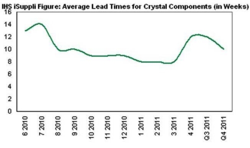
  6 2010 7 2010 8 2010 9 2010 10 2010 11 2010 12 2010 1 2011 2 2011 3 2011 4 2011 Q3 2011 Q4 2011
KHz and MHz Crystals 13 14 10 10 9 9 9 8 8 8 12 12 10

Disruptions spurred by the Japan earthquake and tsunami caused shipments of crystals to be delayed by four weeks in April compared to March, impacting the supply of a critical component employed in products including cell phones and PCs, new IHS iSuppli research indicates. The average lead time for megahertz and kilohertz crystals rose to 12 weeks in April, up 50% from eight weeks in March (figure). Unusually long lead times can lead to delivery delays and short supplies, which could threaten price increases.

"Because Japan is the world’s leading producer of crystals — major suppliers include Epson, NDK and Citizen — the quake crisis will cause pricing for crystals from major Japanese suppliers to climb during the next few weeks," said Rick Pierson.

Among the facilities damaged in the disaster is a supplier’s location in northern Japan that produces crystals for oscillator products. Damage was also sustained by two oscillator suppliers in Fukurawa and Kanagawa, as well as at NDK, which produces crystal oscillator products in its Furukawa, Osaki-city manufacturing site.

On a positive note, status reports from one leading manufacturer of quartz crystals and oscillators that are sold in cylindrical, plastic, metal and ceramic packages show production has restarted at that manufacturer’s Yamanashi, Funehiki-cho, Tamura-shi and Fukushima-ken plants. However, aftershocks and recurring disruptions to the local power grid continue to delay the resumption of normal operations.

For the MEMS industry in general and for Japan’s MEMS sector in particular, the damage was not as severe as initially feared due to a fortuitous accident of geography.  Bouchaud pointed out.

Only three of the 22 most important MEMS and compass fabrication plants in Japan suffered direct damage, IHS iSuppli research shows, although 19 fabs potentially could be affected by the same logistical and power issues impacting all Japanese industries in the calamity’s aftermath. The three damaged facilities belonged to Freescale, Canon Corp. and Texas Instruments (map) pinpointing the location of MEMS and digital compass fabrication facilities throughout Japan.

Click to Enlarge

According to Freescale, the company has decided to close its 150mm fab in Sendai, near the quake’s epicenter, and focus efforts on accelerating the transfer of MEMS production to its 200mm Oak III fab in Texas. Freescale was lucky in that the Sendai fab had been scheduled for shutdown by the end of 2011, and the company already had built buffer inventories. Had it not made this decision in 2009, Freescale and its customers would have been severely hurt, IHS believes.

For Canon, which makes printers and MEMS print heads in the city of Fukushima, site of the nuclear meltdown, production was halted after significant damage to the company’s plant. However, Canon managed to repair the damage very quickly, with the plant completely operational again by the first week of April. As a result, the impact of the disaster on Canon’s MEMS revenue for 2011 is expected to be very modest, IHS iSuppli data indicate.

For its part, Texas Instruments’ Miho fab northeast of Tokyo has undergone the repair of various infrastructure systems for water, gases and chemicals. Full production will resume by the middle of July, with full shipment capacity to commence before September, the company said. Prior to the catastrophe, Texas Instruments already was using multiple fabs for the fabrication of CMOS wafers for DLP MEMS chips, and the company is in a fortunate position to rapidly increase production at its other fabs to compensate for the disruption at Miho.

To learn more about this topic, see the new IHS iSuppli report: The Japanese Disaster and Its Impact on the MEMS and Compass Industry

Also read: MEMS producers in Japan: Facility updates after earthquake

May 5, 2011 — A coordination action on graphene has been funded by the European Commission (EC) to develop plans for a 10-year, EUR1 billion Future and Emerging Technology (FET) flagship. This is an

Click to Enlarge

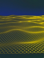
Image. Graphene, a single layer of carbon atoms, may be the most amazing and versatile substance available to mankind. Stronger than diamond, yet lightweight and flexible, graphene enables electrons to flow much faster than silicon. It is also a transparent conductor, combining electrical and optical functionalities in an exceptional way.

ambitious, large-scale visionary research initiative, aiming at a breakthrough for technological innovation and economic exploitation based on graphene and related two-dimensional materials.

 Graphene can trigger a smart and sustainable carbon revolution, with profound impact in information and communication technology (ICT) and everyday life. Its unique properties will spawn innovation on an unprecedented scale and scope for high speed, transparent and flexible consumer electronics; novel information processing devices; biosensors; supercapacitors as alternatives to batteries; mechanical components; lightweight composites for cars and planes.

Cambridge’s role, led by Dr Andrea Ferrari of the Department of Engineering, is to develop the science and technology roadmap for the future investment. These will be the structured plans for what new research on graphene and other two-dimensional materials is needed and the routes for the implementation of graphene in industrially viable technologies. The Cambridge team will determine what new facilities should be built in Europe for that.

"Graphene, a truly European technology, [2010 Nobel Prize for Physics winners Andre Geim and Konstantin Novoselov are both of the University of Manchester, UK and natives of Russia; Geim is a Dutch citizen], is at the crossroad between fundamental research and applications. Exploiting the full potential of graphene will have huge impacts on society at large. We are thrilled that the EU Commission shares our view and believes in our focused and open approach to moving forward, at a time when the international community, from United States to Korea, is moving significant resources to strengthen their know-how and facilitate the roadmap to applications," says Dr Andrea Ferrari.

The research effort of individual European research groups pioneered graphene science and technology, but a coordinated European level approach is needed to secure a major role for EU in this ongoing technological revolution.

Click to Enlarge

Photo. Cambridge University’s Dr Andrea Ferrari, Department of Engineering.

The graphene flagship aims to bring together a large, focused, interdisciplinary European research community, acting as a sustainable incubator of new branches of ICT applications, ensuring that European industries will have a major role in this radical technology shift over the next 10 years. An effective transfer of knowledge and technology to industries will enable product development and production.

The graphene flagship includes over 130 research groups, representing 80 academic and industrial partners in 21 European countries. The coordination action is lead by a consortium of nine partners who pioneered graphene research, innovation, and networking activities. Coordinated by Chalmers University of Technology in Sweden, it includes the Universities of Cambridge, Manchester and Lancaster in the UK, the Catalan Institute of Nanotechnology in Spain, the Italian National Research Council, the European Science Foundation, AMO GmbH in Germany, and the Nokia corporation. The advisory council includes Nobel Laureates Andre Geim (University of Manchester), Konstantin Novoselov (University of Manchester), Albert Fert (THALES) and Klaus von Klitzing (Max-Planck Institute), the leading graphene theoretician Francisco Guinea (CSIC, Spain), as well as Luigi Colombo (Texas Instruments, USA) and Byung Hee Hong (SKK University, Korea), both pioneers of graphene mass production and graphene-based product development.

The pilot phase coordination action started May 1. Its main task is to pave the way for the full 10-year EUR1 billion flagship both in terms of the organizational framework and a scientific and technological roadmap for research and innovation. The action plan for the FET Flagship will be submitted in 2012 to the European Commission, aiming for GRAPHENE to be one of the two flagships launched in 2013.

More details on the graphene flagship pilot can be found at www.graphene-flagship.eu

More information on the EU Future Emerging Technology Flagship Initiative is at http://cordis.europa.eu/fp7/ict/programme/fet/flagship/home_en.html

Follow Small Times on Twitter.com by clicking www.twitter.com/smalltimes. Or join our Facebook group

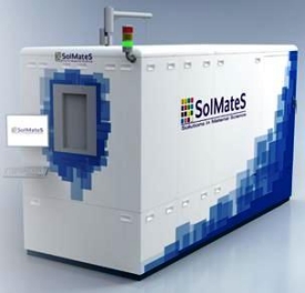
May 5, 2011 — SolMateS received a $3 million investment for the final development phase of their piezoelectric thin film deposition machine, PiezoFlare 1200.

Click to EnlargePrivate equity funds Twente Technology Fund and Participatiemaatschappij Oost Nederland (East-Netherlands Holding Company) invested the capital on April 27, 2011. SolMateS will use the investment to accelerate product development and international expansion for its unique production system.

Piezoelectric layers are to be used in all kinds of miniaturized systems where precise actuation is needed: small motors, radio-frequency micro electromechanical system (RF MEMS) components, micro pumps, etc.

Wet processing is typically used for forming piezoelectric layers, but SolMateS claims that production price and quality cannot meet the high-volume electronic industry standards. 

PiezoFlare 1200 is an automated deposition system for PZT thin films on 6" or 8" wafers, based on pulsed laser deposition. It offers high-yield piezo performance and flexibility for customized PZT compositions. The technology enables high-volume reliable production for PZT thin film deposition.

SolMateS technology has been developed at the University of Twente, and can be used to make MEMS for next-generation mobile electronics, thin film actuators and medical devices.

SolMateS information is available online at www.solmates.nl

Follow Small Times on Twitter.com by clicking www.twitter.com/smalltimes. Or join our Facebook group