Tag Archives: Small Times Magazine

April 7, 2011 – FARS News Agency — Iranian researchers at Mashhad’s Ferdowsi University improved the quality of microextraction by incorporating carbon nanotubes (CNTs).

"We studied trace measurements of environmental samples by gas-liquid chromatography method and applying a new pre-concentration method," Dr. Sarafraz Yazdi, professor at Ferdowsi University, told INIC.

Pre-concentration (extraction) methods demand high consumption of organic solvents, which are expensive and pollute the environment. Scientists have been working on microextraction methods that need no or little amounts of solvent since the 1990s. "One of the non-solvent methods is solid phase microextraction (SPME) in which some solid phase adsorbent (of micrograms) is placed on a capillary fiber of melted silica. This fiber is exposed to the sample and adsorbs it. Afterwards, desorption process takes place in measurement device," Yazdi said.

"In the present study, we placed different adsorbents on fiber through chemical bonding by means of sol-gel methods, which have many advantages over its initial formation. We deposited polyethylene glycol (PEG), a polar compound, on the fiber by sol-gel method. We also managed to introduce functionalized [multiwall carbon nanotubes] MWCNTs to PEG and deposited it on fiber through the aforementioned method. The presence of CNTs resulted in an increase in the effective adsorbent surface and performance of the method."

It is possible to use this method for pre-concentration and measurement of trace environmental samples without using toxic organic solvents.

Follow Small Times on Twitter.com by clicking www.twitter.com/smalltimes. Or join our Facebook group

April 6, 2011 – BUSINESS WIRE — BioScale Inc., a life science company that develops, manufactures, and promotes novel analytical tools enabling advancements in protein research, relocated its corporate headquarters to 4 Maguire Road in Lexington, MA. The move will enable BioScale to scale up its commercial, scientific, R&D, and manufacturing functions in the newly renovated 30,000 square foot facility including Biological Level 2 laboratories and a clean room for its MEMS sensor manufacturing and assembly.

"The positive response we have received from the launch of BioScale’s ViBE product line required us to grow our facility and functionality. We’re building out additional sales, marketing, manufacturing, and application development areas. This growth requires a new, better equipped, and larger facility," commented Mark Lundstrom, BioScale CEO.

BioScale’s current staff includes professional, scientific and manufacturing employees. As the company executes its commercialization plans in 2011, significant employee growth is expected through 2012 with many of the roles in supply chain, sales, marketing, manufacturing and operations.

BioScale is a life science company that develops, manufactures and promotes a proprietary protein analysis technology to accelerate the discovery, development and production of biological and pharmaceutical products. BioScale’s innovative ViBE platform powered by its AMMP (Acoustic Membrane Microparticle) technology enables highly sensitive detection and quantitation of proteins in complex samples used in pre-clinical and clinical research, bioprocess, patient point-of-care and personalized medicine applications. For more information, visit www.bioscale.com.

Follow Small Times on Twitter.com by clicking www.twitter.com/smalltimes. Or join our Facebook group

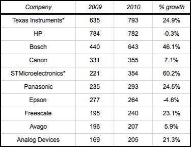
April 7, 2011 – Five years after losing its leadership position in global MEMS supplies, Texas Instruments is back on top thanks to demand for digital light processing (DLP) technology, according to IHS iSuppli’s new 2010 rankings. (Check out 2009 results here and here.)

Click to Enlarge
Top 10 MEMS IDM and fabless manufacturers in 2010 (in US $M). *Does not include MEMS foundry revenue. (Source: IHS iSuppli)

"Texas Instruments’ fortunes in the MEMS market have risen and fallen based on the success of its DLP technology," said Jérémie Bouchaud, director and principal analyst MEMS and sensors for IHS, in a statement. Before 2005 it rode popularity of DLP for rear-projection TV sets, but once those started disappearing so did DLP demand and pricing — its sales slumped 31% from 2005-2009.

Now DLP demand is rising again with the emergence of front-projectors and pico projectors, particularly in China and India, thanks in part to its ability to project 3D content (helps in education applications). Meanwhile, pico projectors produce large displays for their diminutive size (<2lb and <60in3), some of which tan put up 50-in. diagonal images on surfaces (e.g. a wall) using the DLP technology — perfect for advanced mobile devices such as smartphones and netbooks. (A million DLP pico projectors shipped in 2010, iSuppli notes.)

And so, TI enjoyed nearly 25% growth in 2010, third best among the top-10, raking in $793M worth of MEMS. HP’s sales actually declined a fraction to $782M.

A quick snapshot of the other top-10 players:

Hewlett-Packard: The now-No. 2 MEMS chipmaker stagnated due to weakness in the inkjet printhead sector, which contracted -0.8%. HP’s shipments were up, but sales were down due to price erosion, but also HP’s gradual switch to permanent parts, which dented its installed base for disposable print nozzles.

The Bosch Group: The company maintained its No.3 spot and leadership in the sensor segment of MEMS, as sales spiked 46% in 2010. Its consumer MEMS sales (Bosch Sensortec) grew even better (51% to $120M) thanks to accelerometers used in cell phones, in which it outpaced all competitors (ADI 30%, Kionix 22%, ST 10%). Meanwhile, Bosch’s sales growth in auto MEMS outraced the overall sector (45% vs. 32%), due to a rapid rebound in car production, more demand for luxury cars and sensor-equipped cars in Germany, Chinese demand for manifold air pressure sensors, and new government mandates for auto safety systems.

STMicroelectronics: The fastest-growing of the big MEMS suppliers (60%) is tops in the rapidly expanding markets for consumer electronics and cellphone MEMS, notes iSuppli. The company has shipped 50% of consumer accelerometer demand in the past two years (meaning it won’t be able to gain much share anymore), and is seeking new growth drivers e.g. in gyroscopes, which brought in $117M in 2010 and represented 85% of the company’s revenue growth in consumer MEMS. MEMS microphones and MEMS pressure sensors for handsets and tablets should contribute to revenue in 2011, iSuppli notes. Meanwhile, ST also is now shipping low-g accelerometers and introducing high-g accelerometers for airbags.


Learn more in IHS iSuppli’s MEMS website: http://isuppli.com/MEMS-and-Sensors/Pages/Products.aspx

Follow Small Times on Twitter.com by clicking www.twitter.com/smalltimes. Or join our Facebook group

April 6, 2011 — A joint cooperation between three research groups at nanoGUNE reports an innovative method to focus infrared light with tapered transmission lines to nanometer-size dimensions. This device could trigger the development of novel chemical and biological sensing tools, including ultra-small infrared spectrometers and lab-on-a-chip integrated biosensors.

In conventional optical instruments, light cannot be focused to spot sizes smaller than half the wavelength because of diffraction effects. An important approach to beat this diffraction limit is based on optical antennas, which have the ability to concentrate (focus) light to tiny spots of nanometer-scale dimensions, orders of magnitude smaller than what conventional lenses can achieve. Tiny objects such as molecules or semiconductor nanoparticles that are placed into these so-called "hot spots" of the antenna can efficiently interact with light. Thus, optical antennas boost single molecule spectroscopy or the sensitivity of optical detectors. However, the hot spot is bound to the antenna structure, which limits flexibility in designing nano-optical circuits.

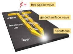
Experiments conducted at nanoGUNE show that infrared light can be transported and nanofocused with miniature transmission lines, consisting of two closely spaced metal nanowires. While lenses and mirrors manipulate light in its form of a free-space propagating wave, transmission lines guide the infrared light in form of a tightly bound surface wave.

Click to Enlarge
Figure 1. Concept and design of the device. Courtesy of Martin Schnell, nanoGUNE.

The researchers at nanoGUNE adapted the concept of classic transmission lines to the infrared frequency range. Transmission lines are specialized cables for carrying radio frequency signals, etc. A simple form consists of two metal wires running closely in parallel, also called ladder line. This structure was widely used to connect a radio receiver or television set to a rooftop antenna. Applied at MHz frequencies, where typical wavelengths are in the range of centimeters to several meters, it is a prime example for transport of energy in waveguides of strongly subwavelength-scale diameter.

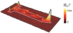
In their experiments, the researchers demonstrated that infrared light can be transported in the same way, by scaling down the size of the transmission lines to below 1um (left panel of the figure). To that end, they fabricated two metal nanowires connected to an infrared antenna. The antenna captures infrared light and converts it into a propagating surface wave traveling along the transmission line. By gradually reducing the width of the transmission line (tapering), the researchers demonstrate that the infrared surface wave is compressed to a tiny spot at the taper apex with a 60nm diameter (right panel of the figure). This tiny spot is 150 times smaller than the free-space wavelength, emphasizing the extreme subwavelength-scale focus achieved in the experiments. The researchers applied their recently introduced near-field microscopy technique (Schnell et al., Nano Lett. 10 3524 [2010]) to map the different electrical field components of the infrared focus with nanoscale resolution.

Click to Enlarge

Figure 2. Near-field microscopy image of the tapered transmission line structure, taken at 9.3µm wavelength (30 THz). It shows the infrared field intensity along the transmission line, revealing the tiny infrared hot spot at the taper apex. Courtesy of Martin Schnell, nanoGUNE.

Nanofocusing of infrared light with transmission lines has important implications in spectroscopy and sensing applications. Connecting a transmission line to the antenna, the infrared light captured by the nanoantenna can be transported over significant distances and nanofocused in a remote place. "This opens new pathways for the development of infrared nanocircuits," says Rainer Hillenbrand, leader of the Nanooptics Group at the nanoscience institute nanoGUNE. The key is that the classical RF concepts still work at IR frequencies, 30 THz, adds Martin Schnell, who performed the experiments.

The fabrication of the transmission lines was carried out by members of the Nanodevices Group and the TEM Laboratory, while the infrared transport and focusing functionality was designed and verified in the Nanooptics Group at nanoGUNE.

Original publication: M. Schnell, P. Alonso-González, F. Casanova, L. Arzubiaga, L. E. Hueso, A. Chuvilin, R. Hillenbrand Nanofocusing of Mid-Infrared Energy with Tapered Transmission Lines, Nature Photonics, advanced online publication, 03 April 2011. DOI: 10.1038/NPHOTON.2011.33, http://www.nature.com/nphoton/journal/vaop/ncurrent/full/nphoton.2011.33.html

Learn more at www.nanogune.eu

Follow Small Times on Twitter.com by clicking www.twitter.com/smalltimes. Or join our Facebook group

April 5, 2011 — Semico chief of technology and blogger Tony Massimini looks at the AKU230 MEMS microphone from Akustica, and finds the tiny device trimmed down by use of semiconductor manufacturing processes rather than traditional MEMS fab.

From the Semico Spin blog:

"The AKU230 is manufactured using conventional CMOS processes. The microphone membrane is a metal/dielectric layer, manufactured just like every other metal/dielectric layer in a CMOS process. The ADC circuitry is located around the membrane and is fabricated at the same time as the membrane during the same conventional CMOS processes. This approach offers savings in silicon area compared to a MEMS microphone fabricated using more traditional MEMS processes.

Some MEMS microphones have an analog audio output. Some have an analog audio output but can provide a digital output using a second semiconductor, essentially an ADC. Akustica MEMS microphones, including the AKU230, are the only MEMS microphones that combine the microphone and the ADC circuitry on one chip, offering a simpler, less expensive solution and one insertion cost rather than two."

Read more from Massimini in his post, "Akustica AKU230: A Tiny Microphone with Huge Potential," at http://www.mapmodel.com/index.php/2011/03/30/akustica-aku230-a-tiny-microphone-with-huge-potential/

Also read "Akustica digital microphone uses smallest fully integrated MEMS"

Follow Small Times on Twitter.com by clicking www.twitter.com/smalltimes. Or join our Facebook group

April 5, 2011 — With the first observation of thermoelectric effects at graphene contacts, University of Illinois researchers found that graphene transistors have a nanoscale cooling effect that reduces their temperature.
 
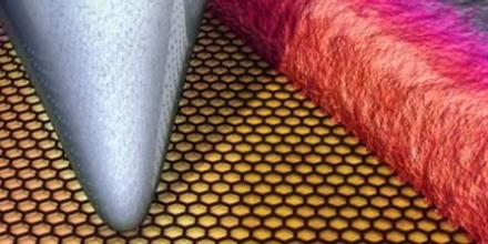
The Illinois team used an atomic force microscope (AFM) tip as a temperature probe to make the first nanometer-scale temperature measurements of a working graphene transistor. The measurements revealed surprising temperature phenomena at the points where the graphene transistor touches the metal connections. They found that thermoelectric cooling effects can be stronger at graphene contacts than resistive heating, lowering the temperature of the transistor.

Click to Enlarge

Image: An atomic force microscope tip scans the surface of a graphene-metal contact to measure temperature with spatial resolution of about 10nm and temperature resolution of about 250 mK.  Color represents temperature data. Alex Jerez, Beckman Institute Imaging Technology Group.

Future computer chips made out of graphene could be faster than silicon chips and operate at lower power, if scientists can grasp a thorough understanding of heat generation and distribution in graphene devices.

The researchers were led by mechanical science and engineering professor William King and electrical and computer engineering professor Eric Pop.

All electronics dissipate heat as a result of the electrons in the current colliding with the device material, a phenomenon called resistive heating. This heating outweighs other smaller thermoelectric effects that can locally cool a device. The speed and size of computer chips are limited by how much heat they dissipate. Computers with silicon chips use fans or flowing water to cool the transistors, a process that consumes much of the energy required to power a device. Graphene’s apparent self-cooling effect means that graphene-based electronics could require little or no cooling.

"In silicon and most materials, the electronic heating is much larger than the self-cooling," King said. "However, we found that in these graphene transistors, there are regions where the thermoelectric cooling can be larger than the resistive heating, which allows these devices to cool themselves. This self-cooling has not previously been seen for graphene devices."

"Our measurements and simulations project that thermoelectric effects will become enhanced as graphene transistor technology and contacts improve," said Pop, who is also affiliated with the Beckman Institute for Advanced Science, and the Micro and Nanotechnology Laboratory at the U. of I.

Next, the researchers plan to use the AFM temperature probe to study heating and cooling in carbon nanotubes (CNTs) and other nanomaterials.

King also is affiliated with the department of materials science and engineering, the Frederick Seitz Materials Research Laboratory, the Beckman Institute, and the Micro and Nanotechnology Laboratory.

The Air Force Office of Scientific Research and the Office of Naval Research supported this work.

The team published its findings in the April 3 online edition of the journal Nature Nanotechnology (http://www.nature.com/nnano/journal/vaop/ncurrent/full/nnano.2011.39.html). Co-authors of the paper included graduate student Kyle Grosse, undergraduate Feifei Lian and postdoctoral researcher Myung-Ho Bae.

Follow Small Times on Twitter.com by clicking www.twitter.com/smalltimes. Or join our Facebook group

April 4, 2011 — Nanoco Group plc (AIM: NANO), cadmium-free quantum dots  manufacturer, produced a 1kg batch of red cadmium-free quantum dots (CFQD) for a major Japanese corporation, which triggers a US$2 million payment to Nanoco by the corporation.

The production of cadmium-free quantum dots on this scale is a major technical achievement that required scalability in Nanoco’s patent-protected technology and the expertise of its production and technical teams.

The 1kg of red CFQD was manufactured to specification at Nanoco’s recently commissioned production facility in Runcorn, Cheshire, UK.

Nanoco expects to be able to demonstrate that green CFQD meet technical milestones within the next few months, which will trigger a milestone payment of US$1 million. This will be followed by the production of 1kg of green CFQD for delivery to the same customer in the second half of 2011. Once validated, the green CFQD will also attract a US$2 million milestone payment.

Also read: Making quantum dots less toxic broadens users’ options 

Nanoco develops and manufactures commercial quantities of quantum dots for use in multiple applications including lighting, solar cells, and biological imaging. Nanoco’s quantum dots, which are free of heavy metals and comply with RoHS legislation, can be combined into a wide range of materials including liquids, polymers and glass. Nanoco forms strategic partnerships with major end users across a range of applications. Nanoco began trading on the AIM market of the London Stock Exchange in May 2009 under the ticker symbol NANO. Learn more at http://www.nanocotechnologies.com/.

Follow Small Times on Twitter.com by clicking www.twitter.com/smalltimes. Or join our Facebook group

April 4, 2011 — A team of researchers from Harvard University and Zena Technologies, led by Kenneth B. Crozier, demonstrated that individual, vertical silicon nanowires can shine in all colors of the spectrum.

The vibrant display, dependent on the diameter of the individual wires, is even visible to the naked eye. The finding has potential for use in nanoscale image sensor devices, offering increased efficiency and the ability to detect color without the use of filters.

Image. To demonstrate the ease of controlling and positioning colorful nanowires, the researchers created a nanoscale-sized tribute to Harvard, designing a pattern resembling the engineering school’s Veritas seal and and spelling out the acronym SEAS. As even small changes in the radius of a wire can alter the color, the Harvard seal turned out to be blue, more suitable for the famous seal of a certain other Ivy League institution.

"In this vertical configuration you can get very strong color effects, and you can tune them over a range of wavelengths of the visible region. The strong effects can be seen right down to the level of the individual wire," says Crozier, John L. Loeb Associate Professor of the Natural Sciences at the Harvard School of Engineering and Applied Science (SEAS). To create the multicolored array of vertical silicon nanowires, the engineers at Harvard and Zena Technologies used a combination of electron beam (e-beam) lithography and inductively coupled plasma reactive ion etching.

A smooth wafer of silicon was plasma etched until all that remained were the vertically protruding nanowires, resembling bristles on a toothbrush. While the nanowires were created in arrays of thousands for convenience, the colors they exhibited were due to the properties of the individual wires, not by the way light was scattered or diffracted in the group.

"Each nanowire acts as a waveguide, like a nano-sized optical fiber, but an optically absorbing one," explains Crozier. "At short wavelengths there is not much optical coupling to the nanowire. At long wavelengths, the coupling is better, but the properties of the waveguide are such that there is not much absorption. In between, there is a range of wavelengths where the light is coupled to the nanowire and absorbed. This range is determined by the nanowire diameter. We made nanowires with diameters of 90, 100, and 130nm that appeared red, blue and green, respectively."

The technology has promising applications. The researchers’ eventual aim is to use the wires in image sensors. Traditional photodetectors in image sensor devices can gauge the intensity of light but not determine its color without the use of an additional filter, which throws away much of the light, limiting the device’s sensitivity.

The researchers hope to address this by fabricating vertical nanowires containing photodetectors above standard photodetectors formed on a silicon wafer. The nanowire and standard photodetectors could each detect a different part of the spectrum of the incident light. By comparing the signals from each, the color could be determined without losing so much of the light.

"With image sensors, every little bit of efficiency counts. Moreover, we even imagine using the colored wires to encode data in a read-only type of information storage," adds Crozier.

The researchers have filed a provisional patent for their work. The finding, published in the March 17, 2011, online edition of Nano Letters (http://pubs.acs.org/doi/abs/10.1021/nl200201b), may be the first experimental report that silicon nanowires can take on a variety of colors depending on their diameter and under bright-field illumination. Previous work has shown that nanowires can take on different colors but only by looking at scattered, rather than directly reflected, light. Crozier’s co-authors included Kwanyong Seo, Paul Steinvurzel, Ethan Schonbrun, Yaping Dan, and Tal Ellenbogen, all from SEAS, and Munib Wober, from Zena Technologies. The study was supported by funding from Zena Technologies and the United States Department of Energy, Office of Science and Basic Energy Sciences. In addition, the research team acknowledges the Center for Nanoscale Systems at Harvard for fabrication work.

Learn more at http://www.seas.harvard.edu/.

Follow Small Times on Twitter.com by clicking www.twitter.com/smalltimes. Or join our Facebook group

April 4, 2011 — Yole Développement released a report on ferroelectric thin films, comprising an overview of the ferroelectric thin films applications and the current and future industrial ferroelectric thin films users in each application. Yole analyzes deposition techniques and materials (PVD, CVD, CSD) trends, and shares production data for ferroelectric thin films (ferroelectric thin film production forecast 2010-2015 in number of wafers, market shares of the different detection techniques globally and by application, market shares of the ferroelectric material).

Ferroelectric thin films have been used for many years in integrated passives devices (IPDs), ferroelectric memories (FeRAM) and MEMS inkjet heads. Such thin films can be used for ferroelectric, piezoelectric or pyroelectric properties.

Ferroelectric materials were considered exotic semiconductor materials in the past. Thanks to better knowledge and industrialization of these materials, they are increasingly used in many new applications, especially in the MEMS field: MEMS wafer-level autofocus, RF MEMS, MEMS ultrasonic transducers infrared sensors, IPD tunable capacitors, and many others.

Figure. Ferroelectric thin films market forecast (in K wafers 6" eq). SOURCE: Ferroelectric Thin Films Report, Yole Développement.

Physical vapor deposition (PVD) is the dominant deposition technique but chemical solution deposition (CSD) techniques will increase its market share greatly, especially in MEMS applications, thanks to its better material composition. PZT, the most well-known ferroelectric material, will keep the leadership on SBT, BST, except if other materials are developed to replace lead, blacklisted by the RoHs European directive.

Driven by existing and new applications, the production of ferroelectric thin films will grow from 881,000 6" eq. wafers in 2010 to 1,263,000 wafers in 2015, meaning a CAGR of +7.5 %. Inkjet head application and IPDs ESD/EMI planar capacitor represent more than 90% of the production in 2010 but other applications will grow strongly to reach globally 26% of the total production in 2015.

Large industrial companies are already using ferroelectric thin films in various applications fields, showing the reliability of this technology:

  • IPDs: NXP, STM
  • MEMS: EPSON
  • FeRAM: Panasonic, Fujitsu, Rhom, Oki, Ramtron

Companies cited in the report:

Argonne lab, Asicon, Avx, BAE, Brother, CEA Le Ripault, Cranfield University, Deplhi, DRS, Epcos, EPFL, Epichem, Epiphotonics, EPSON , FLIR, Fraunhofer IMT, Fraunhofer IPMS, Fujifilm Dimatix, Fujitsu, Gennum, Hammamatsu, Heimann, Holst centre, Hynix, IBM, Imagine Optic, IMEC, Infineon, Inostek, Ipdia, Irisys, KIST, Kojundo lab, Korean Institute of Technology, KTH, L3Com, LAAS, Lemoptix, Lensvector, LG , Matsushita, Maxim, Microsystem lab, Microvision, Mitsubishi Chemical, Murata, Nippon Ceramic, NovioMEMS, NovioMEMS, NXP, Oce, Oerlikon, OKI, Olympus, ON semiconductor, Onchip, Panasonic, Panasonic, Paratek, Philips, Philips Research, Polight, Pondus Instruments, Pulse, Pyreos, Pyreos, Ramtron, Rohm, Samco, Samsung, Semtech, Siemens Medical, Singapore univ, Sintef, Solmates, Sonitor, Sound Design Technology, Steinbeis Transfer centre, ST microelectronics, Suss, Symetrix Corporation, Tango, Technolas perfect vision, Tegal, Texas Instrument, Tezzaron, Thales, Toshiba, Tyndall, Ulis, Ulvac, US Army lab, Vermon, VTT, Western digital, Wispry, Xaar.

In the next 5 years, many new players plan to adopt or evaluate ferroelectric thin films to enter on key markets, from SMEs (Polight, Irisys, NovioMEMS, etc.) to large groups (Océ, Xaar, Delphi, IBM, Philips research, etc).

Ferroelectric Thin Films report from Yole gives an overview of the ferroelectric thin films industry today. It helps devices manufacturers to evaluate the benefits of using ferroelectric think films technologies, identify new business opportunities and partners, monitor their competitor’s advancements. It also helps materials manufacturers, investors, R&D centers and MEMS & Packaging foundries in their developments to identify new opportunities and partners.
 
Authors:
Yann de Charentenay was granted a master degree in physics in INPG in Grenoble and also in Innovation management from Compiegne University. Since 2003, he has worked for Yole Development in the field of MEMS, materials and compound semiconductors. He has contributed to more than 50 marketing and technological analysis.

Dr. Eric Mounier has a PhD in microelectronics from the INPG in Grenoble. Since 1998 he is a cofounder of Yole Developpement, a market research company based in France. At Yole Developpement, Dr. Eric Mounier is in charge of market analysis for MEMS, equipment & material. He is Chief Editor of Micronews, and MEMS’Trends magazines (Magazine on MEMS Technologies & Markets).

Yole Développement is a group of companies providing market research, technology analysis, strategy consulting, media in addition to finance services. More information on www.yole.fr.

Follow Small Times on Twitter.com by clicking www.twitter.com/smalltimes. Or join our Facebook group

Dominique Vicard and Nathalie Sprynski, CEA-Leti, France

For more than a decade, CEA-Leti has been developing microsensors capable of precisely measuring their orientation in relation to the Earth’s gravitational and magnetic fields. Now, Leti is beginning to incorporate arrays of these tiny micro sensors into new kinds of instrumented — or proprioceptive — materials.

The goal of this embedded micro sensor initiative is to capture detailed information about the shape, position and motion of objects fabricated out of these new sensor-laden smart materials, and then use mathematical algorithms to analyze that data and apply it to real-world problems.

Potential applications for proprioceptive materials include:

  • Medicine, where they could help determine the shape and curvature of patients’ spinal columns, or define the best shape for medical belts or wound dressings;
  • Aviation and auto design, where flexible, sensor-equipped ribbons could be used to measure turbulence in the wake of fast-moving aircraft or cars;
  • Computer-aided design (CAD), where applying smart-material wrappers to real objects could generate data for creating detailed numerical models, possibly taking the place of 3D scanners;
  • Sports equipment, where the performance of sails, surfboards, skis or other gear could be monitored, evaluated and improved;
  • Games and virtual reality, where smart clothes could capture players’ complete body moves, allowing them to be totally integrated into the game.
Click to Enlarge
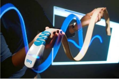
Figure 1. CEA-Leti’s prototype Morphosense tool — embedded with micro sensors — is shown superimposed over a virtual ribbon generated by the system.

To explore the capabilities of proprioceptive materials, Leti researchers have created a ribbon-like prototype called Morphosense, which allows users to remotely capture information about curved shapes in space (Figure 1). Built from a flexible, plastic-coated printed circuit board (PCB) with 16 coupled sensors distributed along the ribbon at 25mm intervals, the system uses a serial-peripheral-interface (SPI) bus to read the sensors’ position data, which is then transmitted wirelessly to a host computer using Bluetooth 2.0 technology.

Two types of sensors are used in tandem to determine the orientation of each point along the Morphosense ribbon. Micro-accelerometer sensors provide data on the ribbon’s orientation to the Earth’s gravitational field as well as acceleration data when the sensor is moving. Micro-magnetometer sensors provide data on the ribbon’s orientation to the Earth’s magnetic field. By embedding both kinds of sensors at each location and combining their orientation information, it is possible to determine the absolute orientation of known points along the ribbon’s surface, which can then be used to generate a mathematical representation of its shape.

The algorithm used to reconstruct the ribbon’s curves requires knowledge of tangential data at each sensor’s position, and the distance between sensors along the ribbon. Based on that, the derivative function can be determined using the arc-length parameter and cubic splines on the unit sphere, and then integrating the three components to retrieve the curve.

Morphosense has enabled Leti to validate the use of proprioceptive materials for both shape capture and motion capture. We still have much to learn about the capabilities and potential uses of embedded micro-sensors, but the technology is looking very promising.

Click to Enlarge
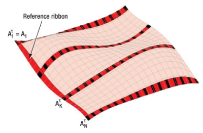
Figure 2. The shape of more-complex surfaces can be acquired using multiple sensor ribbons in a comb structure.

Having proven the concept of capturing relatively simple shapes and motion from ribbons, Leti is turning its attention to more complex three-dimensional surfaces. One promising approach is to embed sensors in either a rectangular mesh, or a comb structure (Figure 2). By reconstructing the curves independently, then adjusting them according to their distribution (based on known information about the system), it should be possible to reconstruct a smooth surface fitting the curves.

Looking ahead, Leti researchers expect to continue miniaturizing these sensors, as well as integrating them into a wider variety of plastic and textile smart materials. Better algorithms should also help improve the interpretation of sensor data and allow the development of more accurate surface models.

Dominique Vicard is Leti’s lab manager for sensors, functionalization and environment. Contact Vicard at +33.4.38.78.55.59; [email protected].

Nathalie Sprynski is a research engineer in mathematics.
     
Follow Small Times on Twitter.com by clicking www.twitter.com/smalltimes. Or join our Facebook group