Tag Archives: Small Times Magazine

PhD student Peter Krogstrup from the Nano-Science Center at the Niels Bohr Institute, University of Copenhagen, developed a theoretical model to explain why and how nanocrystal wires (nanowires) form, in collaboration with researchers from CINAM-CNRS in Marseille. The results have been published in the scientific magazine, Physical Review Letters

Click to Enlarge
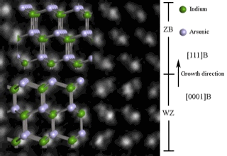
High-resolution image of the crystal structure of an InAs nanowire photographed with an electron microscope. The smallest distance between the indium and arsenic atoms seen in the picture (illustrated with green and gray), is 15 millionths of a millimeter. The nanowire is grown in the direction of the arrow. During growth the crystal structure of the nanowire changes from being hexagonal (WZ) to cubic (ZB). From the crystal orientation seen in the image, the hexagonal structure is characterized by the direction from the In to As atoms changes from layer to layer, while the direction of the cubic structure is always the same.

Krogstrup laid the foundations for a greater understanding of nanowires and potentially improving their performance, which could benefit solar cells and electronics. In the latest edition of Physical Review Letters, he describes how, under certain conditions, nanowires form a crystal structure that were not expected to be possible. See the article here: http://prl.aps.org/abstract/PRL/v106/i12/e125505

"Crystals will always try to take the form in which their internal energy is as little as possible. It is a basic law of physics and according to it these nanowires should have a cubic crystal structure, but we almost always see that a large part of the structure is hexagonal," explains Krogstrup.

He has, as part of his doctoral dissertation, examined the shape of the catalyst particle (a little nano-droplet), which controls the growth of the nanowires. It appears that the shape of the droplet depends on the amount of atoms from group 3 in the periodic system, which make up half of the atoms in the nanowire crystal. The other half, atoms from group 5 in the periodic system, are absorbed by the drop. The atoms organize themselves into a lattice, and the nanowire crystal grows.

"We have shown that it is the shape of the droplet that determines what kind of crystal structure the nanowires obtain and with this knowledge it will be easier to improve the properties of the nanowires," explains Krogstrup. "The crystal structure has an enormous influence on the electrical and optical properties of the nanowires and you would typically want them to have a certain structure, either cubic or hexagonal. The better nanowires we can make the better electronic components we can make to the benefit of us all."

Krogstrup’s research is conducted in collaboration with the firm SunFlake A/S, which is located at the Nano-Science Center at the Niels Bohr Institute, University of Copenhagen. The company is working to develop solar cells of the future based on nanowires.

Learn more at http://www.nbi.ku.dk/english/

Follow Small Times on Twitter.com by clicking www.twitter.com/smalltimes. Or join our Facebook group

March 28, 2011 — A Harvard bioengineer and an MIT aeronautical engineer have created a new device that can detect single cancer cells in a blood sample, potentially allowing doctors to quickly determine whether cancer has spread from its original site.

Click to Enlarge

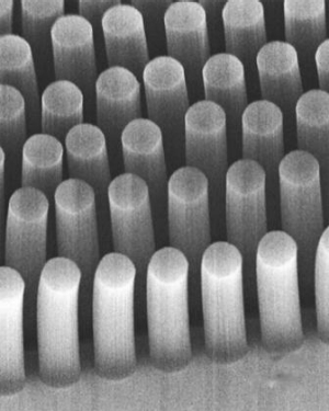
These posts, made of carbon nanotubes, can trap cancer cells and other tiny objects as they flow through a microfluidic device. Each post is 30 microns in diameter. Image: Brian Wardle.

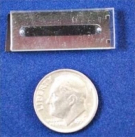
The microfluidic device, described in the March 17 online edition of the journal Small, is about the size of a dime, and could also detect viruses such as HIV. It could eventually be developed into low-cost tests for doctors to use in developing countries where expensive diagnostic equipment is hard to come by, says Mehmet Toner, professor of biomedical engineering at Harvard Medical School and a member of the Harvard-MIT Division of Health Sciences and Technology.

Click to Enlarge

This tiny microfluidic device can separate cancer cells from normal blood cells. Image: Brian Wardle.

Toner built an earlier version of the device four years ago. In that original version, blood taken from a patient flows past tens of thousands of tiny silicon posts coated with antibodies that stick to tumor cells. Any cancer cells that touch the posts become trapped. However, some cells might never encounter the posts at all.

Toner thought if the posts were porous instead of solid, cells could flow right through them, making it more likely they would stick. To achieve that, he enlisted the help of Brian Wardle, an MIT associate professor of aeronautics and astronautics, and an expert in designing nano-engineered advanced composite materials to make stronger aircraft parts.

Out of that collaboration came the new microfluidic device, studded with carbon nanotubes (CNTs), that collects cancer cells eight times better than the original version.

When designing advanced materials, Wardle often uses hollow CNT cylinders whose walls are lattices of carbon atoms. Assemblies of the tubes are highly porous: A forest of carbon nanotubes, which contains 10 billion to 100 billion carbon nanotubes per square centimeter, is less than 1% carbon and 99% air. This leaves plenty of space for fluid to flow through.

The MIT/Harvard team placed various geometries of carbon nanotube forest into the microfluidic device. As in the original device, the surface of each CNT can be coated with antibodies specific to cancer cells. However, because the fluid can go through the forest geometries as well as around them, there is much greater opportunity for the target cells or particles to get caught.

The researchers can customize the device by attaching different antibodies to the nanotubes’ surfaces. Changing the spacing between the nanotube geometric features also allows them to capture different-sized objects: tumor cells (about a micron in diameter), viruses (40nm), etc.

Circulating tumor cells (cancer cells that have broken free from the original tumor) are normally very hard to detect, because there are so few of them — usually only several cells per 1ml sample of blood, which can contain tens of billions of normal blood cells. However, detecting these breakaway cells is an important way to determine whether a cancer has metastasized. "Of all deaths from cancer, 90% are not the result of cancer at the primary site. They’re from tumors that spread from the original site," Wardle says.

Toner’s original cancer-cell-detecting device is now being tested in several hospitals and may be commercially available within the next few years. The researchers are now beginning to work on tailoring the device for HIV diagnosis.

Read the Small abstract and access the article here: http://onlinelibrary.wiley.com/doi/10.1002/smll.201002076/abstract

Courtesy of Anne Trafton, MIT News Office

Follow Small Times on Twitter.com by clicking www.twitter.com/smalltimes. Or join our Facebook group
March 28, 2011 — Studies done by Mark Lusk and colleagues at the Colorado School of Mines could significantly improve the efficiency of solar cells. Their latest work describes how the size of light-absorbing particles — quantum dots — affects the particles’ ability to transfer energy to electrons to generate electricity.

They provide evidence to support a controversial idea, called multiple-exciton generation (MEG), which theorizes that it is possible for an electron that has absorbed light energy, called an exciton, to transfer that energy to more than one electron, resulting in more electricity from the same amount of absorbed light.

The results are published in the April issue of the journal ACS Nano.
 
The idea of quantum dots improving solar cells is not new, as Katherine Derbyshire reported in 2007, but it has yet to be commercialized. For this study, Lusk and collaborators used a National Science Foundation (NSF) supported high-performance computer cluster to quantify the relationship between the rate of MEG and quantum dot size.
 
They found that each dot has a slice of the solar spectrum for which it is best suited to perform MEG and that smaller dots carry out MEG for their slice more efficiently than larger dots. This implies that solar cells made of quantum dots specifically tuned to the solar spectrum would be much more efficient than solar cells made of material that is not fabricated with quantum dots.
 
According to Lusk, "We can now design nanostructured materials that generate more than one exciton from a single photon of light, putting to good use a large portion of the energy that would otherwise just heat up a solar cell."
 
Quantum dots are man-made atoms that confine electrons to a small space. They have atomic-like behavior that results in unusual electronic properties on a nanoscale. These unique properties may be particularly valuable in tailoring the way light interacts with matter.
 
Experimental verification of the link between MEG and quantum dot size is a hot topic due to a large degree of variation in previously published studies. The ability to generate an electrical current following MEG is now receiving a great deal of attention because this will be a necessary component of any commercial realization of MEG.

The research team, which includes participation from the National Renewable Energy Laboratory (NREL), is part of the NSF-funded Renewable Energy Materials Research Science and Engineering Center at the Colorado School of Mines in Golden, CO. The center focuses on materials and innovations that will significantly impact renewable energy technologies. Harnessing the unique properties of nanostructured materials to enhance the performance of solar panels is an area of particular interest to the center.
 
"These results are exciting because they go far towards resolving a long-standing debate within the field," said Mary Galvin, a program director for the Division of Materials Research at NSF. "Equally important, they will contribute to establishment of new design techniques that can be used to make more efficient solar cells."

Learn more at http://www.mines.edu/

Subscribe to Photovoltaics World

Follow Photovoltaics World on Twitter.com via editors Pete Singer, twitter.com/PetesTweetsPW and Debra Vogler, twitter.com/dvogler_PV_semi.

Or join our Facebook group

March 25, 2011 — Despite widespread disruption to Japan’s transportation and utility infrastructure, the country’s digital compass makers report they are working to guarantee that supply of the critical component meets rapidly rising global demand.

IHS iSuppli research indicates that 97% of all digital compass manufacturing worldwide in 2010 was conducted in Japan. The world’s top four suppliers of digital compasses are Japanese firms AKM Semiconductor, Yamaha, Aichi Steel and Alps.

AKM said its main fab that produced electronics compasses for the iPad 2 tablet has not been damaged. The fab is located on Kyushu island, far the south of quake’s epicenter. IHS had indicated the company’s delivery of products potentially could be affected by the same logistical and power supply issues impacting all Japanese industries. AKM said that it uses multiple fabs, including one external source, for the fabrication of its compass, allowing it to mitigate potential logistical challenges.

No. 2 supplier Yamaha said its plant manufacturing digital compasses also was undamaged by the quake and that it is not experiencing the power outages plaguing companies in other parts of the country. Yamaha’s Kagoshima factory is also on Kyushu island. The company said it will work to address logistical problems by changing ports to locations that are not affected by the earthquake and electricity outages.

No. 3 supplier Aichi Steel operates its digital compass fab in Aichi Ken near Nagoya. The company said this facility has suffered no damage and that there has been no delay in shipments. 

Fourth-ranked supplier Alps said that although its compass fab is located in Nagaoka, near the quake zone, the facility appears to in good condition and is operating normally. Read updates on MEMS facilities in Japan.

Click to Enlarge
Year 2006 2007 2008 2009 2010 2011 2012 2013 2014 2015 2009-2014 CAGR
Millions of units 4.1 4.5 9.2 58.0  263.4 470.7 693.2 904.9 1111.2 1,279.3 80.5%
Figure. Global digital compass shipment forecast (Millions of units) SOURCE: IHS iSuppli March 2011.

Global demand for digital compasses is rising rapidly, increasing to 263 million units in 2010, up 354% from 58 million in 2009, reports IHS iSuppli. By 2015, shipments will rise to 1.28 billion, as presented in the attached figure.

Digital compasses are becoming standard in tablets and GPS-enabled cell phones, said Jérémie Bouchaud, director and principal analyst for MEMS (micro-electromechanical systems) and sensors at IHS. He lists Apple Inc.’s iPhone 3 and iPhone 4, devices operating with Microsoft Corp.’s Mobile Windows 7, and Android phones as examples. Move controllers and the upcoming Sony PlayStation Portable (PSP) 2 from Sony Corp also use digital compasses.

Because the calibration of digital compasses regarding electromagnetic interference (EMI) is specific to the systems in which they are used, the components supplied by one company are not easily replaceable with those from another.
 
For more information on the digital compass market, see Bouchaud’s new upcoming report: Digital Compasses Pick up Reigns of Magnetic Sensors Market at http://www.isuppli.com/MEMS-and-Sensors/Pages/Digital-Compasses-Pick-up-Reigns-of-Magnetic-Sensors-Market.aspx?PRX 

Follow Small Times on Twitter.com by clicking www.twitter.com/smalltimes. Or join our Facebook group
March 25, 2011 — University of British Columbia (UBC) chemists developed a model to predict the optical properties of non-conducting ultra-fine particles. The finding could help inform the design of tailored nano-structures, and be of use for remote sensing of atmospheric pollutants, the study of cosmic dust formation, and other fields.

Aerosols and nano-particles play a key role in atmospheric processes as industrial pollutants, in interstellar chemistry and in drug delivery systems, and have become an increasingly important area of research. They are often complex particles made up of simpler building blocks.

Research published this week by UBC chemists in the Proceedings of the National Academy of Sciences indicates that the optical properties of more complex non-conducting nano-structures can be predicted based on an understanding of the simple nano-objects that make them up. Those optical properties in turn give researchers and engineers an understanding of the particle’s structure.

"Engineering complex nano-structures with particular infrared (IR) responses typically involves hugely complex calculations and is a bit hit and miss," says Thomas Preston, a researcher with the UBC Department of Chemistry.

"Our solution is a relatively simple model that could help guide us in more efficiently engineering nano-materials with the properties we want, and help us understand the properties of these small particles that play an important role in so many processes."

"For example, the properties of a more complex particle made up of a cavity and a core structure can be understood as a hybrid of the individual pieces that make it up," says UBC Professor Ruth Signorell, an expert on the characterization of molecular nano-particles and aerosols and co-author of the study.

The experiment also tested the model against CO2 aerosols with a cubic shape, which play a role in cloud formation on Mars.

The research was supported by the Natural Sciences and Engineering Research Council of Canada and the Canada Foundation for Innovation.

Read the paper in the Proceedings of the National Academy of Sciences
www.pnas.org/content/early/2011/03/14/1100170108.abstract

Learn more about UBC at http://www.ubc.ca/

Follow Small Times on Twitter.com by clicking www.twitter.com/smalltimes. Or join our Facebook group

March 25, 2011 – BUSINESS WIRE — Micro electromechanical systems (MEMS) are starting to be the "Swiss Army Knives" of modern consumer electronics: they can take the form of (or be incorporated in) accelerometers, gyroscopes, magnetometers, altimeters, screens, projectors, and microphones. New data from ABI Research indicates that strong growth in the MEMS market over the next five years will result in nearly five billion MEMS being shipped during 2016.

MEMS are found in smartphones, netbooks, media tablets, eReaders, games consoles and handheld gaming platforms, where some of them assist with navigation, dead reckoning, image stabilization, and augmented reality. (Often, consumer devices contain more than one MEMS component.) Still others will underpin new forms of display that use far less power than today’s screen technologies (although initially at greater cost.)

"Initially, smartphones will provide the greatest boost to uptake," notes practice director Peter Cooney, "but if OEMS embrace MEMS displays, they may deliver the strongest overall growth in revenue over time. ABI Research’s MEMS market forecasts depend on device shipments growing as expected. At this point however, we are confident about the prospects for [consumer electronics] CE devices market growth."

The MEMS market is currently split between seven quite specialized major vendors — STMicroelectronics, Asahi Kasei, InvenSense, Bosch, Knowles, Kionix, Freescale Semiconductor — and numerous smaller ones.

"Over time, competition in the MEMS market will result in falling ASPs," says Cooney. "Two of the larger vendors, Bosch and STMicroelectronics, have more diversified product offerings, taking shares across a number of applications. This positions them well to prosper as market conditions change, while other vendors continue to specialize. There is still room for new vendors with new products, however."

ABI Research’s "MEMS in Smartphones and Consumer Electronics" study (http://www.abiresearch.com/research/1006495) analyzes the market opportunity for all of the consumer devices mentioned above in terms of unit volumes, revenues and average selling prices, with forecasts to 2016. ABI Research provides in-depth analysis and quantitative forecasting of trends in global connectivity and other emerging technologies. For more information visit www.abiresearch.com

Follow Small Times on Twitter.com by clicking www.twitter.com/smalltimes. Or join our Facebook group

Giles Humpston, Tessera Inc.

Modern semiconductors are manufactured with feature sizes measured in nanometers. Despite this, semiconductors are not traditionally classed as nanotechnology. A transistor made with 0.5µm technology does not behave in a manner greatly different to one at the 32nm node. To fit with the modern definition of nanotechnology, materials must exhibit properties that are different from those predicted by simple scaling of dimensions. Their properties are influenced by the laws of physics because the feature size is of the same order as the critical size for physical phenomena. Often the difference is manifest as a step change. For example, the radius of the tip of a crack is typically tens of nanometers. Conventional crack propagation and consequent mechanical failure are impossible if the material dimensions are smaller than this.

Nanotechnology is likely to manifest itself in the semiconductor industry in two forms. The first of these is semiconductor devices themselves. It is well known that we cannot go on shrinking devices ad infinitum. Once the device size approaches single atoms quantum physics comes into play — a transistor may, or may not, switch, depending on the prevailing statistics. Building traditional logic gates out of such devices is not sensible, but other decision-making architectures based on quantum devices are being developed. For solid state memories, an important metric of the material used is the ratio of change between the 1 and 0 states. In a well-designed and fabricated flash memory, the ratio will be around 10,000. By exploiting phase change in the nanomaterial graphene, it is possible to obtain ratios of conductivity over 1 million. If realized in a full-sized memory, this would result in a five-fold increase in storage capacity.

In the near term, the most likely application of nanotechnology to semiconductors is in the area of interconnects. Most recent research effort has been concentrated on carbon nanotubes (CNTs). These materials are ballistic conductors with quantum behavior and exhibit exceptionally low electrical resistance. Values around 10E-4 Ohm-cm have been measured, and they have stable current densities as high as 10E12 A/cm2. One of the major causes of power consumption and propagation delay in semiconductor circuits is the RC time constant of interconnects; reducing R by a factor of 10 will confer significant benefits to conventional semiconductors.

Nanotechnology may even replace the ubiquitous gold plating found on the connectors of virtually every plug-in card. Gold is an excellent conductor, but needs to be a minimum thickness to adequately resist corrosion and add durability. The recent spike in the price of gold is having a measurable effect on connector pricing. Nanomaterials are under development that essentially mimic the electrical and mechanical properties of gold. Because they are base metal alloys, their prices are low and remain stable.

It has been said that the twentieth century was the era of the electron, and the twenty-first century will be the era of the photon. USB3, with its optical interface, is an example of this transition. Nanotechnology, by virtue of its dimensions, is conducive to interacting with light. A well-known example is the quantum dot, one use of which is wavelength conversion. These offer the prospect of designing light-emitting semiconductors with high electro-optic efficiency, and changing the emitted light to the desired spectrum using an engineered coating.

Conclusion

Although there are few examples of commercialized semiconductor nanotechnology, there is no doubt that it offers the prospect of significant innovation by providing materials with properties outside of the current domain. The semiconductor industry, with its large and focused R&D base, is likely to be an early adopter. Research journals abound with papers on nanotechnology, offering a tantalizing glimpse of what the future may hold.

Giles Humpston received his PhD and BSc from Brunel U., U.K. and is director of Research and Development at Tessera, 3025 Orchard Parkway, San Jose, CA 95134 USA; [email protected].

March 24, 2011 – Marketwire — Vendum Batteries (OTCBB: VNDB), a US-based battery technology development company, joined the Nano Knowledge Transfer Network (NanoKTN), a Government agency leading and supporting the commercialization of nanotechnologies in the UK.

NanoKTN is about networking, establishing industry collaborations, partner brokering and accessing R&D and commercialization grant schemes from £5,000 to £250,000 ($7,500 to $390,000). Vendum expects to successfully obtain grants and begin further research and development to further improve its battery technology and immediately commence with pre-production prototypes. Through NanoKTN and working closely with universities, start-up companies like Vendum can build strong supply chains.

Fraser Cottington, CEO of Vendum batteries, believes involvement with NanoKTN is a vital component to linking with the academic community in a meaningful and focused way and allows the company to spread the investment risk, by working with in partnership to achieve common goals, in high-tech battery technology and design.

The NanoKTN aims to simplify the nanotechnology innovation landscape by providing a clear and focused vehicle for the rapid transfer of high-quality information on technologies, markets, funding and partnering opportunities. Objectives include: Improved industrial performance through adoption of nanotechnology; Drive knowledge transfer between companies and the research base; Facilitate interactions through networking and event organization; Provide thought leadership and industry input into UK policy and strategy.

Vendum Batteries has a pending patent on a non-toxic, carbon-based light-weight battery. The paper-thin battery contains none of the toxic elements used in conventional batteries and its carbon nanotube and cellulose-based technology makes it entirely biodegradable. For more information please visit www.vendumbatteries.com

Follow Small Times on Twitter.com by clicking www.twitter.com/smalltimes. Or join our Facebook group

March 23, 2011 – BUSINESS WIRE — BioNanomatrix Inc., a developer of nanoscale, single-molecule imaging and analysis platforms designed to reduce the time and cost needed to analyze the genome, has closed a $23.3-million Series B round of equity financing.

Domain Associates, based in Princeton, NJ, and San Diego, CA, led the round, with new investor Gund Investment Corporation and existing investors Battelle Ventures, Innovation Valley Partners and KT Venture Group joining the round.

The company is moving toward commercialization of its nanoAnalyzer platform for whole genome analysis, said R. Erik Holmlin, newly elected president and chief executive officer of BioNanomatrix.

Holmlin noted that BioNanomatrix introduced the nanoAnalyzer 1000 System at the 2010 annual meeting of the American Society of Human Genetics last November and said that the company "has already placed a number of systems with early-access users." Learn more about nanotechnology for life sciences/biomedical applications here.

"BioNanomatrix has made impressive progress in developing and refining its platform technology and testing the nanoAnalyzer in collaboration with leading researchers in the genomics field," said Domain Associates Partner Brian K. Halak, PhD., who joins the company’s Board of Directors.

"This capital infusion enables BioNanomatrix to establish a strong West Coast presence that will provide additional business opportunities and the ability to recruit from a talent base that has established this industry," Dr. Halak continued.

The nanoAnalyzer technology targets integration of genetic information in molecular diagnostics, personalized medicine and biomedical research.

BioNanomatrix is developing and commercializing technologies for analysis of large biological molecules, such as nucleic acids, which are vital to life science research, clinical diagnostic applications and development of new therapeutics. For more information, visit www.bionanomatrix.com.

Follow Small Times on Twitter.com by clicking www.twitter.com/smalltimes. Or join our Facebook group

March 23, 2011 — Researchers at Rice University have created a synthetic material that gets stronger from repeated stress, much like the body strengthens bones and muscles after repeated workouts.

Work by the Rice lab of Pulickel Ajayan, professor in mechanical engineering and materials science and of chemistry, shows the potential of stiffening polymer-based nanocomposites with carbon nanotube (CNT) fillers. The team reported its discovery this month in the journal ACS Nano (see the abstract at http://pubs.acs.org/doi/abs/10.1021/nn103104g).

The complex, dynamic interface between nanostructures and polymers in carefully engineered nanocomposite materials enable this self-enhancing quality. Brent Carey, a graduate student in Ajayan’s lab, found the interesting property while testing the high-cycle fatigue properties of a composite he made by infiltrating a forest of vertically aligned, multiwalled nanotubes (MWCNTs) with polydimethylsiloxane (PDMS), an inert, rubbery polymer. Repeatedly loading the material didn’t seem to damage it at all; the stress made it stiffer.

Carey, whose research is sponsored by a NASA fellowship, used dynamic mechanical analysis (DMA) to test their material. He found that after 3.5 million compressions (five per second) over about a week’s time, the stiffness of the composite had increased by 12% and showed the potential for even further improvement.

"It took a bit of tweaking to get the instrument to do this," Carey said. "DMA generally assumes that your material isn’t changing in any permanent way. In the early tests, the software kept telling me, ‘I’ve damaged the sample!’ as the stiffness increased. I also had to trick it with an unsolvable program loop to achieve the high number of cycles."

Materials scientists know that metals can strain-harden during repeated deformation, a result of the creation and jamming of defects — known as dislocations — in their crystalline lattice. Polymers, which are made of long, repeating chains of atoms, don’t behave the same way.

The team is not sure precisely why their synthetic material behaves as it does. "We were able to rule out further cross-linking in the polymer as an explanation," Carey said. "The data shows that there’s very little chemical interaction, if any, between the polymer and the nanotubes, and it seems that this fluid interface is evolving during stressing."

"The use of nanomaterials as a filler increases this interfacial area tremendously for the same amount of filler material added," Ajayan said. "Hence, the resulting interfacial effects are amplified as compared with conventional composites.

Simply compressing the material didn’t change its properties; only dynamic stress — deforming it again and again — made it stiffer.

Carey drew an analogy between their material and bones. "As long as you’re regularly stressing a bone in the body, it will remain strong," he said. "For example, the bones in the racket arm of a tennis player are denser. Essentially, this is an adaptive effect our body uses to withstand the loads applied to it.

"Our material is similar in the sense that a static load on our composite doesn’t cause a change. You have to dynamically stress it in order to improve it."

Cartilage may be a better comparison — and possibly even a future candidate for nanocomposite replacement. "We can envision this response being attractive for developing artificial cartilage that can respond to the forces being applied to it but remains pliable in areas that are not being stressed," Carey said. Read more about nanotech in medical sciences here.

Both researchers noted this is the kind of basic research that asks more questions than it answers. While they can easily measure the material’s bulk properties, it’s an entirely different story to understand how the polymer and nanotubes interact at the nanoscale.

"People have been trying to address the question of how the polymer layer around a nanoparticle behaves," Ajayan said. "It’s a very complicated problem. But fundamentally, it’s important if you’re an engineer of nanocomposites.

"From that perspective, I think this is a beautiful result. It tells us that it’s feasible to engineer interfaces that make the material do unconventional things."

Co-authors of the paper are former Rice postdoctoral researcher Lijie Ci; Prabir Patra, assistant professor of mechanical engineering at the University of Bridgeport; and Glaura Goulart Silva, associate professor at the Federal University of Minas Gerais, Brazil.

Rice University and the NASA Graduate Student Researchers Program funded the research.

Follow Small Times on Twitter.com by clicking www.twitter.com/smalltimes. Or join our Facebook group