Tag Archives: Small Times Magazine

March 16, 2011 — The Ontario County Local Development Corp. has awarded a $75,000 matching grant to the College of Nanoscale Science and Engineering’s (CNSE) Smart System Technology & Commercialization Center of Excellence (STC), leveraging an additional $75,000 from STC to fund a site master plan for the 57-acre high-tech campus in Canandaigua, NY.

The site master plan, which will be developed by Bergmann Associates, will assist STC as it seeks to become a state-designated "shovel-ready" site, making it a more attractive location for nanotechnology companies looking to locate in Ontario County and the greater Rochester, NY region.

Integrated into CNSE in a partnership between 2 New York Centers of Excellence, STC provides advanced capabilities that enable computer chips to interface with electro-mechanical and biological devices. Leveraged by CNSE’s $7 billion enterprise, the combination gives New York State a global competitive advantage in the development and commercialization of smart system technologies.

"We are optimistic that the high-tech tenant companies based at CNSE’s STC will be expanding in the years to come, and we want to ensure that when those companies are ready, they have the ability and capacity to expand on the STC campus," said Ontario County Economic Developer Mike Manikowski. CNSE’s STC and Moser Baer Technologies have already announced a $20 million public-private partnership to develop the a pilot production line for organic light emitting diodes (OLEDs). Moser Baer Technologies is the United States-based subsidiary of Moser Baer India, Ltd. With its partnership with CNSE’s STC, Moser Baer Technologies is now poised to make its Canandaigua location its first US-based manufacturing operation producing the first OLED manufacturing line for lighting in the U.S.

Moser Baer currently has 9 employees on-site at STC, which will soon increase to 19, and the company expects to create more than 50 jobs by the end of 2012. The company is ramping up its OLED pilot line in space leased in the existing buildings at STC, where Moser Baer Technologies has received support through a Geneva Empire Zone designation. Once the pilot line is successful, it would be advantageous for Moser Baer Technologies to consider locating additional manufacturing capacity here.

"Any future expansion would require additional square footage, so we are very pleased to see Ontario County Local Development Corp. assisting in the planning for future development at this site," said David Newman, VP, Moser Baer Technologies. "Having a shovel-ready location within the tax parcel where we have Empire Zone designation would clearly be an additional incentive to our future growth at this location."

CNSE’s STC assists a variety of partners in industry and government in transitioning new technologies from concept to commercialization. Maintaining a 140,000-square-foot facility with over 25,000 square feet of cleanrooms for micro electro-mechanical systems (MEMS) fabrication and packaging, CNSE’s STC works with small-, medium- and large-sized companies to provide pilot prototyping, low-volume manufacturing and scalable manufacturing. Learn more at http://cnse.albany.edu/Home.aspx

For more information on Ontario County Economic Development programs, visit www.ontariocountydev.org.

Follow Small Times on Twitter.com by clicking www.twitter.com/smalltimes. Or join our Facebook group

March 16, 2011 —  While 2010 was a banner year for the microelectromechanical systems (MEMS) business, with overall growth of 18%, 3 Europe-based companies managed to outperform the market, according to new IHS iSuppli research by analyst Jérémie Bouchaud.

Click to Enlarge
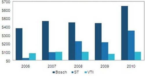
Figure. MEMS revenues for top European companies, not including MEMS foundry revenues. (Millions of US dollars). Source: IHS iSuppli March 2011.

IHS estimates that STMicroelectronics N.V. (STM) revenue for MEMS sensors (not counting its foundry work for inkjet printers) exceeded $353 million in 2010, up 63% from $216 million in 2009.

STMicroelectronics’ strong performance was boosted by $117 million in revenue for its gyroscope business, which also helped the company’s overall consumer MEMS segment achieve 85% revenue growth in 2010. New STM MEMS microphones and MEMS pressure sensor solutions for handsets and tablets paved the way for further growth. Collective revenue from these MEMS products should contribute to STMicroelectronics’ bottom line, beginning in 2011.

Outside of the consumer MEMS segment, STMicroelectronics made significant gains in the high-g accelerometer business for airbags because of a key customer in this area.

The Bosch Group GmbH reached $643 million in MEMS revenue in 2010, up 46% from $440 million in 2009. Consumer revenue for Bosch grew by 51% in 2010 to reach $120 million, up from $80 million in 2009, with accelerometers for handsets as the main source of revenue in this area. Bosch remained the fastest growing company in the consumer accelerometer area, ahead of all its competitors in the consumer MEMS segment. Competitors ADI Inc. expanded 30%; Kionix Inc. grew by 22%; and STMicroelectronics rose by 10%. 

Bosch’s consumer growth should continue, as IHS believes that the company is preparing to launch a 3-axis gyroscope in 2011, even though the company has not made any official comments.

IHS estimates that Bosch’s automotive MEMS revenue grew by 45% in 2010 from $360 million to $523 million, compared to 27% for the rest of the MEMS market. Passenger car production rebounded in 2010, even in countries like Germany, which were expected to be stagnant after the conclusion of the "cash for clunker" schemes. Luxury cars also saw sales increase, spurring a rise in the adoption of mandated technologies such as electronic stability control (ESC) systems, which use MEMS sensors. German cars, especially luxury vehicles that have high electronics content and lots of sensors, are selling well in Asia, particularly China.

Bosch has a very strong position in pressure sensors, especially low-pressure silicon MEMS types used for manifold air pressure sensors in China. Bosch supplies this type of sensor to many cars in the luxury and mid-priced segment. Pressure sensors are being fitted to cars based on the requirement for EURO 4-equivalent emissions regulations set for many Chinese cities. Mandates for safety systems in vehicles, such as ESC systems, are accelerating and beginning to approach full fitment rates for a new series of vehicles in Europe, the United States, Australia, Canada and South Korea in 2011/2012.

While Bosch’s auto MEMS segment won’t grow at the same rate as last year, there is no apparent supply situation that will affect the company’s growth.

Finland-based VTI Technologies Oy also enjoyed strong growth in MEMS, reaching $100 million in 2010, up 35% from $75 million in 2009. VTI attained its previous high level mark of 2007, thanks to a solid performance in the automotive MEMS segment.

Already the No. 1 supplier of low-g accelerometers, VTI began shipping gyroscopes for automotive ESC to Continental in 2010. It also maintained dominance in the medical accelerometer space last year.

Much like Bosch, VTI in 2011 will benefit from the automotive mandates for safety systems, such as ESC systems, in the regions where the mandates are being implemented.

IHS iSuppli provides MEMS and Sensors Research at http://www.isuppli.com/MEMS-and-Sensors/Pages/Products.aspx?MWX

Also read: 
Panasonic, Seiko Epson lead MEMS resurgence in Japan

Follow Small Times on Twitter.com by clicking www.twitter.com/smalltimes. Or join our Facebook group

March 16, 2011 — Recently, we reported that MEMS manufacturing is experiencing a resurgence in Japan, with companies like Panasonic and Seiko Epson leading the charge. In light of the March 11 earthquake and tsunami that devastated northwestern Japan, and led to power outages and transport disurptions across the nation, we provide here a list of MEMS companies that have issued updates on their facilities. To send us your update, email our editorial team via [email protected].

  • Seiko Epson: Epson reports that it has had no employee casualties. Seiko Epson Corporation Sakata Plant and Tohoku Epson Corporation (Sakata, Yamagata Prefecture) operations were suspended due to a power outage caused by the earthquake. Although there was no damage to the buildings, Seiko Epson is still confirming the state of the production facilities, and a date to resume production is not determined.
  • Hitachi: Damages mainly at production bases in Ibaraki prefecture, spanning its power systems, urban planning, IT/control systems, appliances, and automotive systems. The Nikkei daily quoted a company source saying that with power blackouts, "we’ve no idea when production will restart."
  • Panasonic: The company says it is still assessing the quake’s full impact on its operations, but said it could not enter an optical pickup plant in Sendai nor a digital camera facility in Fukushima. Supply and distribution is also partly disabled.
  • Yokogawa Electric Corp.: Manufacturing facilities were not directly impacted by the earthquake or the tsunami as they are distant from the quake epicenter, and sales and service offices and facilities located nearer the epicenter suffered only slight damage. 
  • Hosiden Corp.: Hosiden’s Japanese-language website reports that the company did not suffer major damages to its sites. The company is gathering information on suppliers in northern Japan that could have been affected by the quake. 
  • Omron: No Omron staff were harmed. Omron reports "limited damage to Omron bases and facilities," expecting operations to be back to 100% once transport and electrical infrastructure issues are resolved. Yasu Facility, which produces MEMS, suffered no adverse effects. Omron cautions that there are a large number of Omron suppliers in the disaster area, and that it is taking steps to ensure a viable supply chain. 
  • Sony: Manufacturing operations have been suspended at several manufacturing sites, including Tome Plant, Nakada/Toyosato Sites and Sony Shiroishi Semiconductor Inc., in the Miyagi Prefecture. Sony Corporation Sendai Technology Center (Tagajyo, Miyagi) has ceased operation due to earthquake damage. Undamaged sites have temporarily suspended operations on a voluntary basis, due to widespread power outages.
  • Tamagawa seiki (designer and manufacturer of MEMS gyros) has a plant located in Hachinohe city. There is no damage in the plant and production continues. The company’s employees are safe as well. 

Also read:
Letter from Japan: Update on infrastructure, fab status after earthquake
News from Japan on the Impact of Disasters 
Japan earthquake update: List of facilities impacted 
Update: Japan earthquake’s impact on semiconductor community
Japan earthquake raises questions of solar supply and replacing nuclear power
Japan quake hampering package substrate supplies

Follow Small Times on Twitter.com by clicking www.twitter.com/smalltimes. Or join our Facebook group

Ruby T.S. Lam, John M. Collins, Alexander B. Smetana, Saju Nettikadan, NanoInk Inc.

March 15, 2011 — The ability to place individual cells at defined locations and control their microenvironment has numerous applications in the field of cell biology. Cells respond to their microenvironment and the resulting extracellular signals [1, 2]. The ability to control the cellular microenvironment enables investigation of biochemical and topological cues on various cell behavior, such as cell adhesion, differentiation, and molecular signaling pathways.

Cell morphology has been shown to be closely related to their function at an individual cell level as well as at the tissue and organ level [3]. The long rod shape of myocytes, the elongated shape of neurons, and the spindle shape of fibroblasts are all believed to play a role in the function of their respective tissues. For in vitro systems, these morphologies are influenced by the topographical elements and the geometry of the adhesion pads [4]. Furthermore, biochemical signals from the surface and intercellular signaling from neighboring, interacting cells are critical factors in mediating cell behavior [5]. Controlling the cellular microenvironment is particularly interesting for stem cell studies: commitment of stem cells to different specific lineages has been demonstrated to be dependent on cell shapes that are induced by topography and biochemical cues [6]. Further, the ability to place cells at defined positions on a substrate is critical to the development of cell-based sensing and cell-based drug discovery.

Microcontact printing is currently the most common method for micropatterning cells [7]. This method is used to deposit biomaterials or other chemical entities at defined locations on a surface using a stamp made of a soft material such as Polydimethylsiloxane (PDMS). The limitations of microcontact printing are that not all proteins can be reliably deposited, patterning of multiple materials is also difficult to achieve [8]. The need for a mask and stamp for each pattern makes this method very rigid and not amenable to rapid changes in pattern definition. The surfaces are generally fabricated through silicon microfabrication methods which are not biologically friendly, are expensive, and do not suit to rapid changes in pattern design.

The nanolithography platform, NLP 2000, was designed to provide a simple solution to achieve high precision placement of nano- to micro-sized features with nanoscale precision. The process of deposition of material is based on Dip Pen Nanolithography (DPN), an established method of nanofabrication in which materials are deposited onto a surface using a sharp tip [9, 10]. The tool is capable of patterning a wide range of materials with feature sizes from 50nm to 10µm over an area of 40 x 40mm. The features can be placed with nanoscale precision using a three-axis closed-loop stage.

Click to Enlarge

Figure 1. Acrylic polymer patterns printed on glass substrates by NLP 2000.

The NLP 2000 has been used to deposit proteins, DNA, lipids, polymers, hydrogels, silanes and thiols on many different substrates at subcellular scales. Printing these various materials allows the design and construction of microenvironments for cell-based studies. In this report, we present results demonstrating the capability of the technology to construct topographical and biochemical features at subcellular scales and show the cellular response to these features.
Click to Enlarge

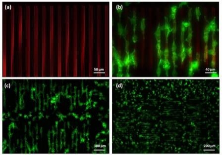
Figure 2. Fluorescence images of (a) patterned acrylic polymer-rhodamine topography; (b) 3T3 cells selectively adhered to and aligned along the direction of the polymer topography; (c) & (d) elongated cells covered 70% of the patterned area (over 1.5 x 0.7mm) at 1.5hrs after cell seeding. Green – actin filaments; red – acrylic polymer patterns.

Influencing cell behavior using topographical features is an attractive strategy for investigating many aspects of cellular function. Features at subcellular dimensions are particularly interesting because it closely mimics the physical features of the in vivo microenvironment. An ultraviolet (UV) curable polymer was used to successfully fabricate topographies on a glass surface. Despite the high ink viscosity (>20,000 cps), the researchers directly deposited it onto a glass surface at subcellular scales with nanoscale precision. Polymer lines that are as fine as 500nm in width and 20nm in height were achieved. Figure 1 shows the bright field images of several polymer patterns constructed on the same chip. These structures were shown to favor cell adhesion. NIH/3T3 fibroblasts (25,000 cells/cm2) were cultured on the substrate in low serum media. Cell attachment was observed on approximately 70% of the patterned features within two hours of cell seeding. Cell morphology was altered due to the patterned polymer on the glass substrate. Figure 2 shows the cellular shapes resulting from the printed polymer topographies that covered a 1.5 x 0.7mm area of the glass substrate. Most cells attached to the topography were selectively aligned on top of the ridges and elongated along the direction of the grating. It is known that focal adhesion dynamics are dictated by topography. Here, spacing between the ridges played an important role in modulating cell spreading and morphology. In this case, cells residing on ridge structures smaller than 2µm showed only minimal focal contact, whereas more pronounced cell elongation and spreading was observed on topographies between 10 to 15µm in total width. In addition, the greatest alignment was observed on grating spaced 20µm apart, and declined as the width decreased. Cells on non-patterned regions also attached to the substrate, but were mostly rounded. On flat surfaces coated with the polymer, the cells bound spread out randomly, demonstrating that the chemical characteristics of the acrylic polymer did not contribute to the elongated morphology. The molecular mechanisms responsible for topography-mediated responses still remain unclear. The data demonstrates that the tool is a flexible platform for construction of topographically patterned substrates for cell biological studies.
Click to Enlarge

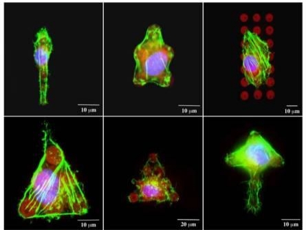
Figure 3. Single 3T3 fibroblasts attached to fibronectin patterns. Cells conform to the shape of the pattern provided. Green – actin filaments; blue – nucleus; red – fibronectin

Another field of interest for cell patterning studies is the cellular response to surface bound biomolecular signals. DPN can be used to fabricate subcellular-scale ligand features for cell studies. The tool enables the user to produce substrates with precise positioning of individual protein ligands, allowing one to control the spacing between ligands with nanometer precision. Here, we demonstrate the technique to directly deposit extracellular matrix proteins onto functionalized glass surfaces. Given the constructive nature of Dip Pen Nanolithography, printing was carried out at ambient conditions, which avoided any protein denaturation due the harsh environmental conditions. A series of fibronectin dot arrays (8μm in diameter and 15μm pitch) were designed and fabricated. The surface was then treated with 2% BSA to prevent nonspecific cell adhesion. NIH/3T3 fibroblasts were added at high density (100,000 cells/cm2) for 30 minutes, at which point non-adherent cells were washed and removed. Cells that remained attached to the fibronectin spots adopted the orientation of the micropatterns. Figure 3 shows fluorescence images of single 3T3 fibroblasts patterned into various shapes using fibronectin. Controlling the shape and location of cells distributed on a patterned substrate at a multicellular scale opens the door to investigate the effects of cell-cell contact in a well-controlled fashion.

Conclusion

Several earlier studies have demonstrated that both topography and biochemical cues are important in regulating cellular behavior. We have demonstrated that Dip Pen Nanolithography, as a fabrication tool, mimics cellular microenvironments in both approaches. It is likely that a truly novel biomaterial scaffold mimicking the in vivo conditions will consist of both topographical and biochemical cues. This nanolithography process can integrate these cues and enable tailor-making of biomimetic microenvironments from subcellular scales to multicell levels.

Acknowledgments
Dip Pen Nanolithography and DPN are registered trademarks of NanoInk Inc.

Ruby T.S. Lam received her PhD/Cambridge University and is an Applications Scientist at NanoInk Inc., 8025 Lamon Avenue, Skokie, IL 60077 USA; ph.: 8477453634; [email protected]

John M. Collins received his PhD/University of Illinois at Chicago and is an Applications Scientist at NanoInk Inc.

Alexander B. Smetana received his PhD/Kansas State University and is an Applications Scientist at NanoInk Inc.

Saju Nettikadan received his PhD/ The Ohio State University and is the director of applications development at NanoInk Inc.

References
1. Shen CJ, Fu JP, Chen CS. Patterning Cell and Tissue Function. Cellular and Molecular Bioengineering, 2008, 1, 15-23.
2. Kulangara K, Leong KW. Substrate topography shapes cell function. Soft Matter, 2009, 5, 4072-4076.
3. Dalby MJ, Childs S, Riehle MO, Johnstone HJH, Affrossman S, Curtis ASG. Fibroblast reaction to island topography: changes in cytoskeleton and morphology with time. Biomaterials, 2003, 24, 927-935.
4. Biggs MJP, Richards RG, Dalby MJ. Nanotopographical modification: a regulator of cellular function through focal adhesions. Nanomed.:Nanotechno., Biol. Med., 2010, 6, 619-633.
5. Lutolf MP, Hubbell JA. Synthetic biomaterials as instructive extracellular microenvironments for morphogenesis in tissue engineering. Nat. Biotechnol., 2005, 23, 47-55.
6. Yim EKF, Pang SW, Leong KW. Synthetic nanostructures inducing differentiation of human mesenchymal stem cells into neuronal lineage. Exp. Cell Res., 2007, 313, 1820-1829.
7. Altomare L, Riehle M, Gadegaard N, Tanzi M, Fare S. Microcontact printing of fibronectin on a biodegradable polymeric surface for skeletal muscle cell orientation. Int. J. of Art. Organs, 2010, 33, 535-543.
8. Ganesan R, Kratz K, Lendlein A. Multicomponent protein patterning of material surfaces. J. of Mater. Chem., 2010, 20, 7322-7331.
9. Piner RD, Zhu J, Xu F, Hong SH, Mirkin CA. "Dip-pen" nanolithography. Science, 1999, 283, 661-663.
10. Sekula S, Fuchs J, Weg-Remers S, Nagel P, Schuppler S, Fragala J, Theilacker N, Franueb M, Wingren C, Ellmark P, Borrebaeck CAK, Mirkin CA, Fuchs H, Lenhert S. Multiplexed Lipid Dip-Pen Nanolithography on Subcellular Scales for the Templating of Functional Proteins and Cell Culture. Small, 2008, 4, 1785-1793.

Follow Small Times on Twitter.com by clicking www.twitter.com/smalltimes. Or join our Facebook group

March 15, 2011 — Engineering researchers at the University of Michigan have found a way to improve the performance of ferroelectric materials, which have the potential to make memory devices with more storage capacity than magnetic hard drives and faster write speed and longer lifetimes than flash memory.

In ferroelectric memory, the direction of molecules’ electrical polarization serves as a 0 or a 1 bit. An electric field is used to flip the polarization, which is how data is stored.

Click to Enlarge

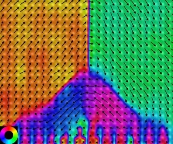
Figure. At the atomic scale, University of Michigan researchers have for the first time mapped the polarization of a cutting-edge material for memory chips. Credit: Chris Nelson and Xiaoqing Pan

With colleagues at U-M and collaborators from Cornell University, Penn State University, and University of Wisconsin, Madison, Xiaoqing Pan, a professor in the U-M Department of Materials Science and Engineering, has designed a material system that spontaneously forms nano-size spirals of the electric polarization at controllable intervals, which could provide natural budding sites for the polarization switching and thus reduce the power needed to flip each bit.

"To change the state of a ferroelectric memory, you have to supply enough electric field to induce a small region to switch the polarization. With our material, such a nucleation process is not necessary," Pan said. "The nucleation sites are intrinsically there at the material interfaces."

To make this happen, the engineers layered a ferroelectric material on an insulator whose crystal lattices were closely matched. The polarization causes large electric fields at the ferroelectric surface that are responsible for the spontaneous formation of the budding sites, known as "vortex nanodomains."

The researchers also mapped the material’s polarization with atomic resolution, which was a key challenge, given the small scale. They used images from a sub-angstrom resolution transmission electron microscope (TEM) at Lawrence Berkeley National Laboratory. They developed image processing software to accomplish this.

"This type of mapping has never been done," Pan said. "Using this technique, we’ve discovered unusual vortex nanodomains in which the electric polarization gradually rotates around the vortices."

A paper on the research, titled "Spontaneous Vortex Nanodomain Arrays at Ferroelectric Heterointerfaces" is available online at NanoLetters. Access the article here: http://pubs.acs.org/doi/abs/10.1021/nl1041808

This research is funded by the Department of Energy, the National Science Foundation and the U.S. Army Research Office.

The University of Michigan College of Engineering is home to 11 academic departments, numerous research centers and expansive entrepreneurial programs. The College plays a leading role in the Michigan Memorial Phoenix Energy Institute and hosts the world-class Lurie Nanofabrication Facility. Find out more at http://www.engin.umich.edu/.

Follow Small Times on Twitter.com by clicking www.twitter.com/smalltimes. Or join our Facebook group
March 14, 2011 – BUSINESS WIRE Plasma-Therm LLC, plasma etch and deposition equipment supplier, secured majority shareholder status of Advanced Vacuum, a vacuum and thin film equipment provider headquartered in Sweden. Both operations have partnered to create a strategic alliance with complementary etch and deposition systems that support the needs of R&D through production environments.

The partnership aims to expand an established sales and service network and enable additional resource allocation to Advanced Vacuum’s product development thanks to additional support and funding through Plasma-Therm. Both companies plan to extend their market reach in the areas of dedicated R&D systems, failure analysis and non-clustered platforms.

"With this transaction we anticipate expansion into applications that will leverage Advanced Vacuum’s capabilities for custom vacuum equipment design and fabrication…and their expertise in control system upgrades," said Abdul Lateef, CEO at Plasma-Therm.

Advanced Vacuum provides a focused portfolio of services and products for the vacuum and thin film technology industries. Offerings include vacuum and electronics control systems and open load plasma etch and deposition systems. Advanced Vacuum is also a key principal OEM equipment supplier for northern Europe through representation of Edwards Vacuum, Advanced Energy and Entegris. To learn more about Advanced Vacuum, visit their website at www.advanced-vacuum.se.

Plasma-Therm is a supplier of advanced plasma process equipment offering etch and deposition technologies. Plasma-Therm systems support various specialty markets including solid state lighting, thin film head, MEMS, photomask and compound semiconductor. To learn more about Plasma-Therm, visit www.plasmatherm.com.

Follow Small Times on Twitter.com by clicking www.twitter.com/smalltimes. Or join our Facebook group

March 11, 2011 — Oxford Nanopore Technologies Ltd signed an exclusive agreement with Harvard University’s Office of Technology Development for the development of graphene for DNA sequencing. Under the terms of the agreement, Oxford Nanopore has exclusive rights to develop and commercialize methods for the use of graphene for the analysis of DNA and RNA, developed in the Harvard laboratories of Professors Jene Golovchenko, Daniel Branton, and Charles Lieber.

Graphene is a single-atom thick lattice of carbon with high electrical conductivity. These properties make it an ideal material for high resolution, nanopore-based sequencing of single DNA molecules.

The agreement adds to an existing collaboration between Oxford Nanopore and Harvard that spans basic methods of nanopore sensing through to the use of solid-state nanopores. Oxford Nanopore will also continue to support fundamental nanopore research at Harvard.

Dr Gordon Sanghera, CEO of Oxford Nanopore Technologies, explained that the "groundbreaking research at Harvard lays the foundation for the development of a novel solid-state DNA sequencing device."

"Oxford Nanopore is probably best known for protein nanopores,” continued Dr Sanghera. "However, today’s agreement highlights that we are increasing our investment in solid-state nanopores by adding graphene to our existing portfolio of solid-state nanopore projects and collaborations."

The Harvard team and collaborators used graphene to separate two chambers containing ionic solutions, and created a hole — a nanopore — in the graphene. The group demonstrated that the graphene nanopore could be used as a trans-electrode, measuring a current flowing through the nanopore between two chambers. The trans-electrode was used to measure variations in the current as a single molecule of DNA was passed through the nanopore. This resulted in a characteristic electrical signal that reflected the size and conformation of the DNA molecule. The work was presented in a 2010 Nature publication (S. Garaj et al, Nature Vol 467,doi:10.1038/nature09379).

Graphene is believed to be the thinnest membrane able to separate two liquid compartments from each other. This is an important characteristic for DNA sequencing; a trans-electrode of this thickness would be suitable for the accurate analysis of individual bases on a DNA polymer as it passes through the graphene.

Nanopore techniques aim to improve substantially the cost, power and complexity of DNA sequencing. While first-generation technologies in development at Oxford Nanopore use nanopores made by porous proteins, subsequent generations will use synthetic solid-state materials such as silicon nitride. Challenges remain in industrial fabrication of synthetic nanopores with the required dimensions and electronic properties. Graphene offers a potential solution due to its strength, dimensions, electrical properties and future potential for low-cost manufacturing.

Oxford Nanopore Technologies Ltd is developing a novel technology for direct, electronic detection and analysis of single molecules using nanopores. The company also has collaborations for the development of solid-state nanopores. Learn more at http://www.nanoporetech.com/

Nature publication: Graphene as a subnanometre trans-electrode membrane, S. Garaj, W. Hubbard, A. Reina, J. Kong, D. Branton & J. A. Golovchenko. Nature Vol 467,doi:10.1038/nature09379 (Sept 2010)
This publication describes the use of graphene as a trans-electrode, detecting a DNA strand as it passes through a hole in the graphene sheet. A sheet of graphene was stretched over a silicon-based frame, and inserted between two separate liquid reservoirs. An electrical voltage was applied between the reservoirs and when a nanopore was formed in the graphene this allowed the flow of an ionic current through the nanopore.

This current could be measured as an electrical current signal using the trans-electrode properties of graphene. Double-stranded DNA strands were added to one chamber and electrophoretically driven through the nanopore. This created a characteristic electrical signal that reflected the size and conformation of the DNA molecule. Graphene is thin enough to interact with individual nucleotides on a DNA strand as it passes through the nanopore, and therefore suitable for further development as a solid state DNA sequencing tool. Graphene Graphene is a single atom thick sheet of carbon – one layer of graphite. The carbon atoms are arranged in a hexagonal planar structure. Graphene has extremely high strength-to-weight ratio and has higher electrical conductivity than silicon. The material has been proposed as suitable for many future applications including a range of electronic nanodevices, batteries, touch screens, transmitters and receivers for broadband communications.

Follow Small Times on Twitter.com by clicking www.twitter.com/smalltimes. Or join our Facebook group

March 11, 2011 — Paper association TAPPI’s nanotechnology groups have created a new International Nanotechnology Division. This Division will focus on nanotechnology for renewable materials, including the advancement of R&D for nanocellulose and applications such as coatings, plastics, digital displays, military body armors, and medical implants.

The nanotech division will comprise producers, academia, government, consulting companies, suppliers and others in the industry.

Creation of the new division builds on the six years of success with TAPPI’s International Conference on Nanotechnology for Renewable Materials, held this year in Washington DC, June 6-8 (www.tappinano.org). The event has accelerated the development of standards for nanocellulose, such as bringing TAPPI’s ANSI Accredited Standards process to support ISO’s Technical Committee on Nanotechnology. The International Nanotechnology Division will augment this event by supporting technical developments and broader industry understanding of the value of nanocellulosic nanomaterials. It will also address emerging issues around environmental health, safety and risk assessment in the development of commercial nano-based products. 

The new International Nanotechnology Division is TAPPI’s eleventh division. Each division works to share specific knowledge and provide solutions for the global industry through a variety of member benefits, products, services, and volunteer opportunities, including publications, events, education and training.

TAPPI is now recruiting volunteers for the International Nanotechnology Division who can help identify advancements in renewable nanocellulose materials research, development and commercialization. To learn more or join this division of TAPPI, email Mary Ann Cauthen, TAPPI Member Group Coordinator, at [email protected]

TAPPI is the leading association for the worldwide pulp, paper, packaging and converting industries. Visit www.tappi.org for more information.

Follow Small Times on Twitter.com by clicking www.twitter.com/smalltimes. Or join our Facebook group

March 10, 2011 — A Brigham Young University (BYU) physics student and his professor have a new method of growing tiny machines from carbon molecules.

BYU physics professor Robert Davis and his student Taylor Wood started by patterning the iron seeds of the BYU logo onto an iron plate. Next, they send heated gas flowing across the surface, and a batch of carbon nanotubes (CNT) springs up.

"It’s a really fragile structure at this point — blowing on it or touching it would destroy it," Davis said. "We developed a process to coat and strengthen the tubes so that we can make microstructures that have practical applications."

Another student, Jun Song, used the process to make devices that quickly and neatly separate the various chemicals contained in a solution. The approach using carbon nanotubes is more precise than current chemical separation methods because it gives more control over the channels that the fluids flow through.

The BYU researchers are building several kinds of micro-machines, including actuators, switches, and humidity-detecting cantilevers. Next on their agenda is to create filtration devices.

The company US Synthetic licensed the commercial rights from BYU. Another company, Moxtek, also entered into a licensing agreement with BYU for applications to their X-ray windows.

The technique is detailed by the BYU physicists in a new study published in the scientific journal Advanced Functional Materials. Physics professor Richard Vanfleet and chemistry professor Matthew Linford also contributed to the project and appear as co-authors on the new study. Two researchers from US Synthetic also appear as co-authors. 

Learn more at http://www.byu.edu/webapp/home/index.jsp

Follow Small Times on Twitter.com by clicking www.twitter.com/smalltimes. Or join our Facebook group
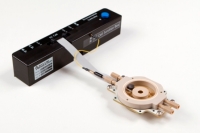
March 10, 2011 — Asylum Research, scanning probe and atomic force microscopy (SPM/AFM) technology provider, launched the Electrochemistry Cell (EC Cell) for its MFP-3D AFMs. The EC Cell is a versatile platform for electrochemical experiments combined with AFM imaging, accommodating samples (working electrodes) including metal cylinders, flat conducting samples, and even conducting thin films on insulating substrates.

Click to EnlargeThe platform enables studies of deposition, oxidation, corrosion, and mass transfer of metals and other materials. Nanoscale topographical changes can be precisely monitored in situ as induced by electrochemical reactions. The cell provides for heating from ambient to 60°C (optional) and can be operated in a fully sealed configuration. 

Asylum Research developed the EC Cell in collaboration with Professor Richard Compton of the University of Oxford (UK) to conduct electrochemical experiments and develop images of the changes occurring to the sample, said Dr. Maarten Rutgers, product manager.

The MFP-3D offers independent piezo positioning in all three axes, combined with low noise closed-loop feedback sensor technology. The MFP-3D enables top and bottom sample viewing and easy integration with most commercially available inverted optical microscopes. 

Asylum Research is a technology leader in atomic force and scanning probe microscopy (AFM/SPM) for both materials and bioscience applications. Learn more at www.AsylumResearch.com.

Follow Small Times on Twitter.com by clicking www.twitter.com/smalltimes. Or join our Facebook group