Tag Archives: Small Times Magazine

February 28, 2011 – Alchimer, nanometric deposition technology provider for through-silicon vias (TSVs), semiconductor interconnects, micro electro mechanical systems (MEMS), and other electronic applications, announced that the Centre de Collaboration MiQro Innovation/MiQro Innovation Collaborative Centre (C2MI) has licensed its suite of products.

The C2MI, which includes a state-of-the-art MEMS facility, was launched in 2009 by Université of Sherbrooke in Bromont Technoparc, Quebec, Canada. The center’s 200mm MEMS and 3D wafer-level-processing (WLP) equipment will enable its members to test a variety of materials for MEMS production.

Alchimer’s suite of products and its Electrografting (eG) technology will support the center’s 3D MEMS programs. Electrografting is Alchimer’s electrochemical process that enables the growth of extremely high-quality polymer and metal thin films.

The MiQro Innovation Collaborative Centre and its members are pushing the design rules in this space, at the leading edge of 3D integration in MEMS, said Alchimer CEO Steve Lerner.

"Alchimer Electrografting technology dramatically increases yields in MEMS, 3D-IC and on-chip interconnects, and provides strong support for work in advancing the technology for 3D MEMS manufacturing with a cost-effective approach," said Luc Ouellet, vice-president of R&D at Teledyne DALSA Semiconductor, a pure-play MEMS foundry.

Alchimer develops and markets innovative chemical formulations, processes and IP for the deposition of nanometric films used in a variety of microelectronic and MEMS applications, including wafer-level interconnects and TSVs (through-silicon vias) for 3D packaging. For more information, visit www.alchimer.com.

The MiQro Innovation Collaborative Centre (C2MI) is an original partnership between Université de Sherbrooke and microelectronics industry leaders. The initial investment (building and research equipment) of $218.45 million is supported by Industry Canada ($82.95 million), by the ministère du Développement économique, de l’Innovation et de l’Exportation ($94.9 million), by the town of Bromont (taxe exemption for 10 years, a $15 million value), by the founding partners and equipment suppliers ($40.6 million). Visit www.c2mi.ca to learn more.

Follow Small Times on Twitter.com by clicking www.twitter.com/smalltimes. Or join our Facebook group

February 28, 2011 — Various industries — such as aerospace, sporting goods manufacturers, construction – are incorporating technological advances using nanocomposites, with extraordinary results. Epoxy materials are being transformed into stiffer, lighter, and stronger materials thanks to the addition of fullerenes and carbon nanotubes (CNTs). Dongsheng Mao, Applied Nanotech, Applied Nanotech Holdings (APNT), describes a process involving multi-walled carbon nanotubes (MWCNTs) that have stronger mechanical properties yet remain lightweight and within end-product cost parameters.

These epoxy materials frequently appear in industry as fiber reinforced plastics (FRP). The properties of these new epoxy/carbon nanotube composites are generally not easily transferred to the FRP. However, using this new composite, APNT achieved a 31% improvement in the flexural strength of the final FRP and similar improvements are expected in compression strength.
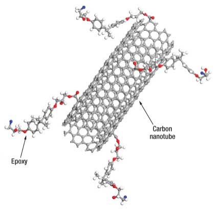
Click to Enlarge
Figure 1. Schematic diagram of carbon nanotube (CNT) reinforced epoxy. Strong bonding between functionalized carbon nanotubes and epoxy is formed to significantly improve mechanical properties of the composites.

The epoxy/CNT nanocomposite material has properties tailored to 3D assembling, thanks to an ability to uniquely handle blocks of CNTs. Large-volume applications include golf club shaft and sports racquet manufacture. Manufacturers using this material can decrease product weight while maintaining strength, portability, and flexibility. Sporting goods products are only the first application area.

The role carbon nanotubes play

Only 1-2% of the product is carbon nanotubes, yet they improve mechanical properties. By dispersing and functionalizing CNTs individually, ANI spread the CNTs throughout an epoxy matrix such that, when force is applied on the final product, a part of that stress is transferred to the CNTs.

CNTs possess unique mechanical properties. Their stiffness, strength and resilience exceed similar properties of any current material, with the potential for fundamentally new material systems, in particular, structural nanocomposites. Unfortunately, their integration with polymer matrices presents new technical challenges.

CNTs tend to aggregate with each other to form ropes or bundles due to intrinsic van der Waals forces associated with their high surface energy. De-agglomeration and dispersion of CNTs in various media has been recognized as one of the major challenges of commercial CNT adoption. Traditional methods such as sonication, high-shear mixing, stirring, and surfactants are often used in lab-scale quantities to disperse CNTs, but those methods have proven ineffective on an industrial scale. Although surface functionalization of CNTs has improved dispersions, the results for the mechanical properties of CNT-reinforced nanocomposites also depend on mixing procedures and carbon fiber-reinforced polymer (CFRP) manufacture methods.

Transferring interesting and unique nanocomposite properties to CFRPs can be realized only by successfully integrating functionalized CNTs into more complex structures. Using CNTs as a reinforcing component in polymer composites requires the ability to tailor the nature of the CNT walls to control the interfacial interactions between the CNTs and the polymer chains.

Applied’s CNT achieved over 40% improvement in both flexural and compression strength for epoxy/carbon nanotube composites. Chemical and mechanical modification and CNT functionalization, for them to be accepted and integrated properly into the epoxy matrix, were essential.

Click to Enlarge
Figure 2. Yonex’s new golf clubs (EZONE) are made using Applied Nanotech, Inc’s patented technology (www.yonex.co.jp).

Commercializing new CNT products

At times, companies worry about sharing propriety research information. Without all of the pertinent data, it is difficult to clearly understand how to apply nanotechnology methods to achieve the desired result. In cases like this, if the CNTs are not functionalized properly, or epoxy penetration into the fiber is suboptimal, the final material will have visible defects and no mechanical enhancement. Communication between industry and research entities is therefore essential to develop commercially viable products, as APNT demonstrates with this sporting goods partner.

Cost is always a manufacturing consideration. Even the greatest design improvements fail in the market if consumer cost is prohibitive. We advise clients to carefully examine how nanotechnology is applied to a project. In the past, single-wall nanotubes (SWCNTs) have enabled some great results, but costs were exorbitant. Today, functionalized CNT prices are dropping considerably, so we focused on MWCNTs. The results were significantly improved compression strength, flexural strength, modulus, impact strength, and vibration damping factor compared with epoxy.

We have demonstrated that the functionalization and dispersion methods used in CNT-reinforced epoxy and other thermosetting nanocomposites is a promising technology that can be expanded into many other fields, including aviation, defense, aerospace, marine, and cleantech.

Dongsheng Mao received his Ph.D from Chinese Academy of Sciences with a background of Materials Science and Engineering and is director of the Nanocomposite Division at Applied Nanotech. Inc., Applied Nanotech Holdings (Stock Symbol: APNT), 3006 Longhorn Blvd., Suite 107, Austin, TX 78758; [email protected]. Dongsheng Mao is director of Applied Nanotech Inc.’s Nanocomposite Division.

Follow Small Times on Twitter.com by clicking www.twitter.com/smalltimes. Or join our Facebook group

February 25, 2011 — The Smart System Technology & Commercialization Center of Excellence (STC) of the College of Nanoscale Science and Engineering (CNSE) of the University at Albany will spearhead a pair of national initiatives valued at $6 million to develop, fabricate and deploy innovative nano-sensing technologies in support of critical applications in the military and energy sectors.

STC has been awarded a $3 million contract by the U.S. Space and Naval Warfare Systems Command (SPAWAR) in San Diego, CA to develop, fabricate and test a variety of smart sensor technologies to enhance military intelligence gathering by soldiers in the field. Featuring a combination of integrated circuits with active sensing technologies, they include intelligence, surveillance and reconnaissance (ISR) sensors; inertial sensors, acoustic sensors and energy-harvesting components; opto-electro-mechanical systems; and resistive heaters.

Dr. Richard Waters, fabrications manager for SPAWAR Systems Center San Diego, said, "The critical effort to develop and deploy innovative technologies that not only assist the U.S. military in achieving its strategic objectives, but also keep our fighting forces out of harm’s way, will be strengthened through this partnership between SPAWAR and CNSE’s Smart System Technology & Commercialization Center of Excellence."

STC is also working with the Electric Power Research Institute (EPRI) of Palo Alto, CA to design a groundbreaking wireless sensor for monitoring potentially damaging vibration of components on high-speed power generating equipment. This innovative on-line sensor can potentially save the industry hundreds of millions of dollars in lost availability and repair costs, as well as improving safety. STC will further leverage this work into a $3 million initiative through the U.S. Department of Energy (DOE) to develop a full system. Prototypes are expected this summer for the sensor system, which will initially monitor blades in steam turbines, but is expected to be expanded to include blades in wind turbines, helicopters, jet engines and turbines that power ships and submarines, among other applications.

Steven Hessler, Program Manager at EPRI, said, "The smart sensor technologies STC is developing, using their advanced design and fabrication capabilities, should provide our members with new opportunities to deliver power reliably, efficiently and cost-effectively."

Work for both programs will take place at STC’s facilities and be supported by CNSE’s Albany NanoTech Complex.

CNSE SVP and CEO Dr. Alain Kaloyeros said, "The UAlbany NanoCollege, through its Smart System Technology & Commercialization Center of Excellence, is delighted to collaborate with SPAWAR and EPRI on these exciting initiatives enabled by nanoscale innovations. These new partnerships highlight STC’s expanded focus on developing smart sensor technologies and solutions to address areas of critical national need, including the military and energy sectors."

CNSE VP for disruptive technologies and STC executive director Paul Tolley said, "We are excited to work with both SPAWAR and EPRI to develop innovative smart sensor technologies that address vital challenges for the U.S. military and the energy industry. These programs demonstrate the growing importance of smart sensor technologies to enable essential system improvements, from the state-of-the-art systems used by SPAWAR to enhance military performance while protecting our soldiers, to the program with EPRI that will ensure reliable power generation with significant financial savings."

Integrated into CNSE in a partnership of two of New York’s Centers of Excellence, STC provides certified cleanroom space for fabrication and packaging of MEMS devices that leverages CNSE’s $7 billion Albany NanoTech Complex, which features 80,000 square feet of Class 1 capable cleanrooms equipped with leading-edge tools and state-of-the-art capabilities to accelerate 21st century nanotechnology innovations. The UAlbany CNSE college is dedicated to education, research, development, and deployment in the emerging disciplines of nanoscience, nanoengineering, nanobioscience, and nanoeconomics. The UAlbany NanoCollege houses a fully integrated, 300mm wafer, computer chip pilot prototyping and demonstration line within 80,000 square feet of Class 1 capable cleanrooms.

An expansion currently in the planning stages is projected to increase the size of CNSE’s Albany NanoTech Complex to over 1,250,000 square feet of next-generation infrastructure housing over 105,000 square feet of Class 1 capable cleanrooms and more than 3,750 scientists, researchers and engineers from CNSE and global corporations. For information, visit www.cnse.albany.edu.

The College of Nanoscale Science and Engineering’s Smart System Technology & Commercialization Center assists small and large companies transition new technologies from concept to manufacturing. STC maintains a 140,000-square-foot facility with over 25,000 square feet of cleanrooms for micro electromechanical systems (MEMS) fabrication and packaging, and works with large and medium-sized companies to help them bring new technologies to market; with small companies ready to transition from prototype and low-volume manufacturing to scalable manufacturing; and with various federal agencies to develop technology solutions to areas of critical national need, including smart prosthetics and improvised explosive device (IED) detection. For more information, visit www.stcmems.com.


Follow Small Times on Twitter.com by clicking www.twitter.com/smalltimes. Or join our Facebook group

February 25, 2011 — New research from the University of Pennsylvania demonstrates a more consistent and cost-effective method for making graphene, the atomic-scale material that has promising applications in a variety of fields, and was the subject of the 2010 Nobel Prize in Physics.

As explained in a recently published study on Feb. 10 in the journal Chemistry of Materials, a Penn research team was able to create high-quality graphene that is just a single atom thick over 95% of its area, using readily available materials and manufacturing processes that can be scaled up to industrial levels.

"This research is pushing closer to the ultimate goal, which is 100%," said the study’s principal investigator, A.T. Charlie Johnson, professor of physics. "We have a vision of a fully industrial process."

Other team members on the project included postdoctoral fellows Zhengtang Luo and Brett Goldsmith, graduate students Ye Lu and Luke Somers and undergraduate students Daniel Singer and Matthew Berck, all of Penn’s Department of Physics and Astronomy in the School of Arts and Sciences.

Graphene is a chicken-wire-like lattice of carbon atoms arranged in thin sheets a single atomic layer thick. Its unique physical properties could lead to major advances in solar power, energy storage, computer memory and a host of other technologies. But complicated manufacturing processes and often-unpredictable results currently hamper graphene’s widespread adoption.

One of the more promising manufacturing techniques is chemical vapor deposition (CVD), which involves blowing methane over thin sheets of metal. The carbon atoms in methane form a thin film of graphene on the metal sheets, but the process must be done in a near vacuum to prevent multiple layers of carbon from accumulating into unusable clumps. "If you need to work in high vacuum, you need to worry about getting it into and out of a vacuum chamber without having a leak," Johnson said. "If you’re working at atmospheric pressure, you can imagine electropolishing the copper, depositing the graphene onto it and then moving it along a conveyor belt to another process in the factory."

The Penn team’s research shows that single-layer-thick graphene can be reliably produced at normal pressures if the metal sheets are smooth enough. Johnson’s group used commercially available copper foil in their experiment. "The fact that this is done at atmospheric pressure makes it possible to produce graphene at a lower cost and in a more flexible way," Luo, the study’s lead author, said.

Other methods make expensive custom copper sheets in an effort to get them as smooth as possible; defects in the surface cause the graphene to accumulate in unpredictable ways. Instead, Johnson’s group electropolished their copper foil, making it smooth enough to produce single-layer graphene over 95% of its surface area.

Working with commercially available materials and chemical processes that are already widely used in manufacturing could lower the bar for commercial applications.

"The overall production system is simpler, less expensive, and more flexible," Luo said.

This research was supported by Penn’s Nano/Bio Interface Center through the National Science Foundation. Learn more at www.upenn.edu

Follow Small Times on Twitter.com by clicking www.twitter.com/smalltimes. Or join our Facebook group

February 25, 2011 – Global production value of nanocarbon products — single-walled carbon nanotubes (SWNT), multi-walled carbon nanotubes (MWNT), fullerenes, graphene, carbon nanofiber, and nanodiamonds — will triple over the next four years in value, and by orders-of-magnitude in actual production, according to a recent analyst report.

Production of carbon nano products totaled about 710 tons in 2010, for a rough value of $435M, calculates Innovative Research and Products Inc. (iRAP). The company predicts that will swell to 9,300t and $1.3B by 2015.


2010
2015
AAGR %
(2010-2015)
SWNT 180 320 12.2
MWNT 105 700 46.7
Fullerenes 61 60 -0.33
CNF 88 144 10
Graphene 0.75 48 130
TOTAL
435
1272
24

Nanocarbon production value (in US $M) according to types. (Source: iRAP)

Inside the numbers, iRap finds some key trends:

  • Production closing the capacity gap. Those surging output numbers for nanocarbon products suggest partially solving a more important problem: massive overcapacity. In 2010, production capacity for these materials was 4065t — actual output of 710t translates to 17% capacity utilization. (Output was only about 500t in 2009, and 340t in 2008.) But by 2015, iRap sees this gulf closing, with actual production doubling over the period to exceed 9300t (a 67.3% annual growth rate), translating to an 80% utilization based on the 12,300t of projected capacity.
  • Despite surging output and capacity, demand hasn’t really caught up yet, iRap notes, but suppliers want to be ready to match future demand seen coming in the next 5-10 years. Contributing to that demand spark, overall prices are coming down: the firm projects prices for all nanocarbon products will fall by an average of ~12%/year from 2010-2015.

  • Nanotubes leading the way. Multiwalled carbon nanotubes (MWNT) will pace the growth, says iRap: 390t of global capacity in 2008, 1500t in 2009, >3400t in 2010, and 9400t by 2015. But single-walled carbon nanotubes (SWNT), the most expensive of the lot, are the key to the kingdom; they "are much more difficult to produce than MWCNTs," iRap notes, and are seen replacing silicon as the ubiquitous electronic starting material within the next decade or so.
  • Asia is production home. Asia’s production capacity for both types of nanotubes (SWNT and MWNT) is 2×-3× higher than North America and Europe combined, says iRap. Japan is a leader in MWNT production (driven by demand for lithium-ion battery electrodes) but China and Korea are catching up fast.

  • Share of nanocarbon production value according to types, 2015 vs. 2010. (Source: iRAP)


February 24, 2011 — A lab at Rice University has developed an efficient method to disperse nanotubes in a way that preserves their unique properties and adds more. The technique allows inorganic metal complexes with different functionalities to remain in close contact with single-walled carbon nanotubes (SWCNT) while keeping them separated in a solution.

That separation is critical to manufacturers who want to spin fiber from nanotubes, or mix them into composite materials for strength or to take advantage of their electrical properties. The ability to functionalize the nanotubes at the same time may advance imaging sensors, catalysis and solar-activated hydrogen fuel cells.

A batch of nanotubes can stay dispersed in water for weeks on end. Keeping carbon nanotubes from clumping in aqueous solutions and combining them with molecules that add novel abilities have been difficult for scientists exploring the use of these highly versatile materials. They’ve tried attaching organic molecules to the nanotubes’ surfaces to add functionality as well as solubility. But while these techniques can separate nanotubes from one another, they take a toll on the nanotubes’ electronic, thermal and mechanical properties.

Angel Marti, a Rice assistant professor of chemistry and bioengineering and a Norman Hackerman-Welch Young Investigator, and his students reported this month in the Royal Society of Chemistry journal Chemical Communications that ruthenium polypyridyl complexes are highly effective at dispersing nanotubes in water efficiently and for long periods. Ruthenium is a rare metallic element.

Marti and his team created ruthenium complexes by combining the element with ligands, stable molecules that bind to metal ions. The resulting molecular complex is part hydrophobic (the ligands) and part hydrophilic (the ruthenium). The ligands strongly bind to nanotubes while the attached ruthenium molecules interact with water to maintain the tubes in solution and keep them apart from one another.

Another key turned out to be moderation. Marti and co-authors Disha Jain and Avishek Saha — Jain is a former postdoctoral researcher in Marti’s lab, and Saha is a graduate student — were originally eyeing ruthenium complexes as part of a study to track amyloid deposits associated with Alzheimer’s disease. "We started to wonder what would happen if we modified the metal complex so it could bind to a nanotube," Marti said. "That would provide solubility, individualization, dispersion and functionality."

"Avishek put this together with purified single-walled carbon nanotubes (created via Rice’s HiPco process) and sonicated. Absolutely nothing happened. The nanotubes didn’t get into solution — they just clumped at the bottom.

"That was very weird, but that’s how science works — some things you think are good ideas never work."

Saha removed the liquid and left the clumped nanotubes at the bottom of the centrifuge tube. "So I said, ‘Well, why don’t you do something crazy. Just add water to that, and with the little bit of ruthenium that might remain there, try to do the reaction.’ He did that, and the solution turned black."

A low concentration of ruthenium did the trick. "We found out that 0.05% of the ruthenium complex is the optimum concentration to dissolve nanotubes," Marti said. Further experimentation showed that simple ruthenium complexes alone did not work. The molecule requires its hydrophobic ligand tail, which seeks to minimize its exposure to water by binding with nanotubes. "That’s the same thing nanotubes want to do, so it’s a favorable relationship," he said.

Marti also found the nanotubes’ natural fluorescence unaffected by the ruthenium complexes. "Even though they’ve been purified, which can introduce defects, they still exhibit very good fluorescence," he said.

He said that certain ruthenium complexes have the ability to stay in an excited state for a long time — about 600 nanoseconds, or 100 times longer than normal organic molecules. "It means the probability that it will transfer an electron is high. That’s convenient for energy transfer applications, which are important for imaging," he said.

That nanotubes stay suspended for a long time should catch the eye of manufacturers who use them in bulk. "They should stay separated for weeks without problems," Marti said. "We have solutions that have been sitting for months without any signs of crashing."

The Welch Foundation supported the research.

More information can be found at www.rice.edu

Follow Small Times on Twitter.com by clicking www.twitter.com/smalltimes. Or join our Facebook group

February 24, 2011 – FARS News Agency — Iranian researchers at Kashan University calculated the physical and mechanical properties of multi-walled carbon nanotubes (MWCNT) and nitride-Bohr nanotubes in a move to help improve the design of arms for nano-robots.

The body of the nano robot has joints or fixed points around which arms move. This research studies the various stability types of two-walled or multi-walled carbon nanotubes in an elastic environment around these moving parts. "What distinguishes this study from all other researches carried out recently is the presentation of Pasternak model that considers the effect of shear forces applied by the elastic environment to the two-walled carbon nanotubes," Dr. Ali Qorbanpour Arani, a lecturer at University of Kashan, told the Iran Nanotechnology Initiative Council.

Arani, a member of the Nanoscience and Nanotechnology Research Center of University of Kashan added, "In this study, the physical and mechanical properties of the multi-walled carbon and nitride-Bohr nanotubes were determined. The properties can be used in the design of nano-robots’ arms. In addition, they can be used as intelligent nanotubes due to their piezoelectric properties by using electrical field on them, and they can control the rotation and movement or the kinetic of the movement in the arms and neck of the nano-robot."

"Taking into account the fact that nanotubes are usually studied in an elastic environment, in order to calculate the forces applied to nanotubes, which include vertical and shear forces, we used Winkler model (for studying the vertical forces) and Pasternak model (for the vertical and shear forces) to obtain more precise results," Qorbanpour Arani concluded.

Copyright 2011 Fars News Agency. All Rights Reserved

Follow Small Times on Twitter.com by clicking www.twitter.com/smalltimes. Or join our Facebook group

February 24, 2011 NEC Corporation (NEC; TSE: 6701) announced the development of a compact sensor that measures the power consumption of electronic devices and delivers this information to energy management systems, without needing an external power supply or battery. An independent power supply to the sensor is achieved through energy harvesting.

Energy harvesting converts energy from a surrounding area into electrical energy without the need of an external power source. Although this method can be used to convert magnetic fields emitted from power lines into an operating electric supply, energy harvesting can only convert about 1mW of power, which is insufficient for sensors currently that are used to measure power consumption and send data to an energy management system.

These newly developed sensors consume less than 1mW of power by leveraging an original circuit design that enables them to both measure the power consumption of electric devices and transmit data. As a result, these sensors can provide visibility of electrical device power consumption without the need of an external energy supply. Furthermore, since these sensors do not require data transmission devices, such as wireless interfaces, they may be easily managed and produced in a compact size.

Research by NEC:
Development of a monitoring sensor that enables high precision, low power, continuous real time monitoring and measurement of current waveforms that are consumed by electronic devices. These measurements identify distinctions between each device and provide detailed information on energy consumption and operational status that also enable the detection of unusual operating conditions.

Development of a data transmission circuit that uses the measurement object’s AC power line as a transmission path to send current waveform information to a management system in order to calculate power consumption. This has eliminated the need for wireless transmission devices to send data to energy management systems, which has increased usability and enabled the miniaturization of sensors.

Development of a control circuit that manages the power consumption of sensors by alternately operating the monitoring circuit and data transmission circuit described in the points above. The control circuit ensures that the same level of power is consumed both when the monitoring circuit is operated and when the data transmission circuit is operated. The control circuit accomplishes this by concentrating its operations during the same time as the, relatively low power consuming, monitoring circuit’s operations. Conversely, the control circuit’s operations are stopped while the, relatively high power consuming, data transmission circuit is operating. As a result, these new sensors can measure current waveforms and transmit data while consuming less than 1mW of power, which enables them to operate without the use of an external power supply.

These new sensors, which enable the visualization of power consumption while being free from battery or transmission device maintenance, are suitable for a wide range of electronic devices. Looking forward, NEC will continue to develop power management systems for electronic devices that capitalize on these sensors and contribute to the realization of a low-carbon society.

NEC will present the results of this research on February 22 at the IEEE International Solid State Circuits Conference (ISSCC 2011), held February 20 -24 in San Francisco, California, U.S.A.
More from ISSCC:

NEC Corporation enables IT and network technologies that benefit businesses and people around the world. For more information, visit NEC at http://www.nec.com.

Follow Small Times on Twitter.com by clicking www.twitter.com/smalltimes. Or join our Facebook group

February 23, 2011 – BUSINESS WIRE — USHIO America Inc. will start marketing the nano-imprint vacuum ultra violet (VUV) ashing system "CHIPs (Compact HiPower System)" in the US in March. Incorporated into nano-imprint lithography (NIL) equipment to be used for fabricating circuit patterns of LEDs, MEMS, functional films, and biochips, the CHIPs allows non-contact and damage-free cleaning, surface improvement, and ashing of templates and workpieces.

NIL is a lithography technology that transfers a circuit pattern by directly imprinting a template (or mold) with the circuit pattern on a workpiece (a resist-coated silicon, sapphire, or film substrate). It has the advantage of being a low-cost process, allowing large-area pattern transfer, and being suitable for mass-production. NIL already has been put into practical use for fabricating circuit patterns with a line width at a µm level. NIL has evolved with further research and development efforts to establish a finer-pattern process technology at a nm level.

Today, the NIL process faces challenges caused by putting a workpiece into contact with a template (contamination with resist residue, fill failures, deteriorating release properties), which are obstacles for fabricating finer patterns as well as enhancing productivity. Wet- or dry-cleaning equipment needs to be separately installed to clean the templates by removing them from the NIL equipment. Wet-clean equipment has an insufficient cleaning capability, causes a risk of generating chemical residue, and requires additional processes (such as drying and waste disposal). The dry-cleaning equipment using plasma, meanwhile, has disadvantages in that it causes damage to a workpiece and requires additional components (such as a vacuum chamber).

Click to EnlargeUSHIO developed its new nano-imprint VUV ashing system "CHIPs" by applying and optimizing its lighting-edge technologies to NIL to achieve non-contact and damage-free high cleaning power using VUV light. In addition, the CHIPs can be incorporated into the NIL equipment to allow reduced downtime and increased automation.

USHIO will exhibit and participate in the "SPIE Advanced Lithography 2011" conference, to be held February 27 through March 3, 2011, at the San Jose Convention Center and San Jose Marriot in San Jose, CA, on Booth 428.

USHIO AMERICA INC. provides specialty and general illumination lighting solutions. For further information, visit www.ushio.com.

USHIO INC. handles a variety of lighting equipment, halogen lamps for OA, UV lamps for exposure used in semiconductor/liquid crystal display/LED manufacturing processes, high-brightness discharge lamps for data projectors and xenon lamps for movie projectors. For further information, visit www.ushio.co.jp.