Tag Archives: Small Times Magazine

February 7, 2011 — The Higgs boson is being sought at CERN’s Large Hadron Collider (LHC). According to physicists at Madrid’s Institute for Material Science, ripples in atom-thick graphene arise from a spontaneous symmetry-breaking process similar to that which separated the weak and electromagnetic forces in the early universe. This graphene research could shed light on the Higgs boson particle

At the high energies of the early universe, the weak nuclear force and the electromagnetic force are thought to converge into one electroweak force. As the temperature of the universe fell below a certain point, the two forces suddenly became separate. This "electroweak symmetry breaking" can be explained in terms of a field — the Higgs field — shifting from an effectively empty high-energy state to its ground state, filling space with a field that gives some particles their mass.

The yet-to-be-detected Higgs boson is the particle associated with vibrations of this field, and is currently being sought in the LHC. What drives the Higgs field between the high-energy and ground states? Although the parameters in the Standard Model of particle physics can be adjusted to force the symmetry-breaking, it is possible that the Higgs field may not need any coaxing. Pablo San-Jose and colleagues at Madrid’s Institute for Material Science now argue that studies of the emergence of ripples in graphene could shed some light on the process.

Solid State Technology editor Robert Haavind has speculated that Higgs boson research and discovery could land physicists a Nobel prize. The 2010 Nobel Prize-garnering (in Physics) material graphene may be a stepping stone to that discovery.

Graphene loses some symmetry in the transition from a flat shape to a rippled one, in the same way as the "activation" of the Higgs field is tied to the breaking of the electroweak symmetry. "Measuring the rippling of graphene under variable tension could give us information about the details of the intrinsic condensation of the Higgs," San-Jose says.

Working with colleagues Francisco Guinea and Jose Gonzalez, San-Jose claims to have shown that the energy landscape of graphene rippling in 2D, and that of the Higgs field in 3D, are described by similar "Mexican hat" potentials. Like a sombrero, the potential energy starts high in the center but quickly falls away to a minimum in any direction. The negative curvature at the top ensures that symmetry will break spontaneously – any push from the centre sends the system down towards a stable point in the brim, just where the edge of the hat begins to climb again.

In the case of graphene, the negative curvature is a result of how graphene responds to being stretched or compressed. In particle physics, negative curvature is a result of the relationship between the Higgs field and the "bare" mass of the Higgs boson. In order to be unstable, this bare mass must be imaginary – the Higgs boson acquires a real, effective mass when the field reaches its true stable ground state.

According to San-Jose, studying how graphene responds to compression by buckling into ripples could give hints about how the Higgs condenses. Small, spontaneous ripples in the absence of compression, for example, would suggest that the Higgs field may condense without requiring an imaginary bare mass for the Higgs boson. Experiments could also probe the structure of the potential in cases where the ripples are larger, providing information about mathematically difficult details of the Higgs quantum field theory.

Vitor Pereira, a condensed-matter physicist from the National University of Singapore, is interested in the Spanish team’s explanation for how these ripples arise in graphene, which it sees as being via interactions between electrons and deformities in the structure that soften the material. He suggests that graphene’s structure might be tunable through the control of electrons.

Pereira adds that graphene’s properties may mimic other experimentally difficult processes, such as how particle–antiparticle pairs arise in the vacuum. Although some researchers are sceptical about accuracy of such models, he thinks otherwise. Graphene, arguably the simplest of the condensed-matter systems, is a good testbed for such sophisticated ‘high-energy’ phenomena, he says.

The work is reported in Phys. Rev. Lett. 106 045502. Access the article at http://prl.aps.org/abstract/PRL/v106/i4/e045502
Abstract: We show that the interaction between flexural phonons, when corrected by the exchange of electron-hole excitations, may drive the graphene sheet into a quantum critical point characterized by the vanishing of the bending rigidity of the membrane. Ripples arise then due to spontaneous symmetry breaking, following a mechanism similar to that responsible for the condensation of the Higgs field in relativistic field theories, and leading to a zero-temperature buckling transition in which the order parameter is given by the square of the gradient of the flexural phonon field.

Courtesy of Kate McAlpine, science writer based in the UK, http://physicsworld.com

Follow Small Times on Twitter.com by clicking www.twitter.com/smalltimes. Or join our Facebook group
 

By Debra Vogler, senior technical editor

February 7, 2011 — Researchers at imec — Danae Delbeke, photonics technology developer, INTEC (imec’s associated laboratory at Ghent U.) and Francesco Pessolano, manager, NVISION Program, imec — discuss announcements made in conjunction with Photonics West (January 25-27, 2011, San Francisco, CA) regarding the research consortium’s NVISION program (for advanced imaging solutions) and silicon.

Listen to the interviews here: Download (iPhone/iPod users) or Play Now

Pessolano describes the NVISION Program (announced 6 months ago) and explains in detail some of the changes that had to be made to standard CMOS processing to accommodate the requirements for hyperspectral imaging and smart lenses. For example, imec uses the Fabry-Perot effect instead of the complex optics (i.e., splitting light using prisms) used in conventional hyperspectral imaging; the result is a more cost-effective solution that is easily integrated. Pessolano said that the new imaging solution is 100× cheaper and 10-60× faster than the conventional imaging system.

 Click to Enlarge  Click to Enlarge

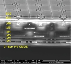
Figure 1. Cross-sectional view of integrated micro-mirror array, showing the mirrors (SG1 electrode and SG2 structural layer) on top fo the 6 layers (M1-M6) of Al interconnect. SOURCE: imec

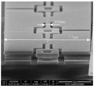
Figure 2. Top view of individual mirror, size 7.7µm, spacing 300nm, hinge width 350nm, phase step in center. SOURCE: imec

Imec’s MEMS-based solution for smart lenses (two mirrors that deform to accomplish the zoom function) uses micro-mirrors (Figs. 1, 2). Pessolano discusses why it is necessary to control the tilt angles in an "analog" manner rather than digital. He also explains the materials selection and other factors (such as fill factor, and space constraints) important to the solution. The changes required a complete redesign of the micro-mirror topology, taking about 18 months for the redesigned MEMS-based device.

 Click to Enlarge  Click to Enlarge

Figure 3. Advanced passive silicon photonics processes. SOURCE: imec

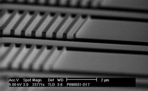
Figure 4. Highly efficient grating couplers realized by amorphous silicon deposition.

Imec’s silicon photonics platform allows for the miniaturization of complex photonic functions on a single chip, i.e., a dense integration of photonics and electronics (Figs. 3, 4). Delbeke observes that reusing the wafer scale processes for silicon photonics, especially if the volumes are high, is cost-effective. Imec has also been standardizing the main optical building blocks for additional cost efficiency.

Follow Small Times on Twitter.com by clicking www.twitter.com/smalltimes. Or join our Facebook group
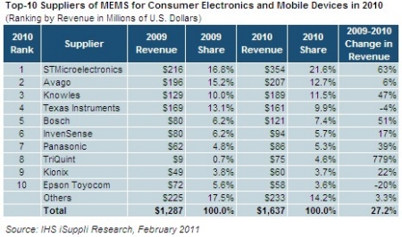
February 4, 2011 — Apple’s iPad and the Android-based tablets, along with other media tablets, make up the fastest growing microelectromechanical system (MEMS) sector in the consumer electronics and mobile segments, says IHS iSuppi researcher Jérémie Bouchaud. MEMS sales for tablet use is predicted to increase nearly 400% YOY. Cell phones remain the largest sector for MEMS adoption, however.

Click to Enlarge

Sales of MEMS for use in tablets will rise to $140.4 million this year, up 373% from a mere $29.7 million in 2010. By 2014, tablets will become the second-largest application for MEMS sensors in the consumer and mobile space after cell phones, with revenue of $280 million.

"With their focus on providing compelling user interfaces, tablets are emerging as a major growth area for MEMS," said Jérémie Bouchaud, principal analyst for MEMS and sensors at IHS. "MEMS accelerometers and gyroscopes play a key role in tablets, utilized not only for automatic screen rotation and tilt compensation for the compass but also for motion-based user interfaces. MEMS filters such as bulk acoustic wave duplexers are also used in 3G tablets, and pressure sensors and MEMS microphones likewise will join the fray in 2011. All this will result in the expansion of MEMS sales in tablets and help drive the growth of the overall market for MEMS consumer electronics devices and mobile devices."

The consumer electronics and mobile market for MEMS in 2011 will grow by more than 25%. This will nearly equal the growth rate of 2010, when the industry recovered robustly following the economic crisis of 2009.

Revenue in 2011 for MEMS sensors and actuators used in various consumer and mobile devices — including cell phones and tablets — will reach $2.07 billion, up 26.2% from $1.64 billion last year. The growth will continue the 27.1% expansion of 2010 after the market retreated to single-digit growth in 2009 given the economic slowdown. The five-year market prospects call for growth by a factor of nearly three to $3.71 billion in 2014, up from $1.13 billion in 2009, translating into a solid compound annual growth rate (CAGR) of 23.6% during the time period.

Among consumer and mobile devices, cell phones will command the largest share of MEMS use in 2011, projected to reach $1.1 billion. Cell phone sales will continue to expand during in the years to come, and both conventional handsets as well as smart phones will employ an ever-larger number of MEMS devices.

Video gaming, while still the second-largest application for consumer MEMS this year at $229.7 million, is on a path of steady decline because of market saturation and declining prices for MEMS devices for the sector. Revenue will rebound in 2014 when next-generation gaming platforms are introduced, breathing new life into the segment.

Other important markets for consumer MEMS in 2011 are cameras, projectors, laptops, MP3 players and televisions.

Top MEMS devices

Utilized in devices like mobile phones and tablets but also in gaming, cameras, laptops and remote controls, accelerometers this year will continue to hold the pole position among all consumer MEMS devices. Revenue from accelerometers in 2011 will exceed $500 million, with cell phones accounting for the majority of accelerometer shipments from now until at least 2014.

Catching up fast to accelerometers are 3-axis gyroscopes, in second place this year with revenue also in excess of $500 million, thanks to their use in the iPhone 4 from Apple and the PlayStation Move game controller from Sony Corp as well as in handheld game players, e.g. the Nintendo 3DS and the new PSP from Sony. By 2014, accelerometers and gyroscopes will figure in a neck-and-neck finish, with the combined market for both devices reaching a market-commanding $1.6 billion.

Other best-selling MEMS devices in 2011 will include bulk acoustic wave filters, which will benefit from the increasingly widespread use of next-generation 4G wireless technology; MEMS microphones, predominant in noise-suppression technology made popular by the Droid smart phone from Motorola Corp as well as the iPhone 4; and digital light processing (DLP) chipsets, currently enjoying a renaissance with the advent of tiny pico projectors.

Read "Consumer MEMS: The Sky is the Limit!" at http://isuppli.com/MEMS-and-Sensors/Pages/Consumer-MEMS-The-Sky-is-the-Limit.aspx?PRX

IHS iSuppli technology value chain research and advisory services range from electronic component research to device-specific application market forecasts, from teardown analysis to consumer electronics market trends and analysis and from display device and systems research to automotive telematics, navigation and safety systems research. More information is available at www.isuppli.com. IHS (NYSE: IHS) is a source of information and insight in energy, economics, geopolitical risk, sustainability and supply chain management.

Follow Small Times on Twitter.com by clicking www.twitter.com/smalltimes. Or join our Facebook group

February 3, 2011 — The same properties that make engineered nanoparticles attractive for numerous applications — small as a virus, biologically and environmentally stable, and water-soluble — also cause concern about their long-term impacts on environmental health and safety (EHS). One particular characteristic, the tendency for nanoparticles to clump together in solution, is of great interest because the size of these clusters may be key to whether or not they are toxic to human cells. Researchers at the National Institute of Standards and Technology (NIST) have demonstrated for the first time a method for producing nanoparticle clusters in a variety of controlled sizes that are stable over time so that their effects on cells can be studied properly.*
 

Click to Enlarge
Figure. Transmission electron micrograph of gold nanoparticles clustering in solution. The distance between the two red arrows is approximately 280 nanometers, some 200 times smaller than the diameter of a human hair. The individual nanoparticles are approximately 15nm in diameter, about the distance across three side-by-side sodium atoms. Credit: A. Keene, U.S. Food and Drug Administration

In their tests, the NIST team made samples of gold, silver, cerium oxide and positively charged polystyrene nanoparticles and suspended them separately in cell culture medium, allowing clumping to occur in each. They stopped the clumping by adding a protein, bovine serum albumin (BSA), to the mixtures. The longer the nanoparticles were allowed to clump together, the larger the size of the resulting cluster. For example, a range of clustering times using 23nm silver nanoparticles produced a distribution of masses between 43 and 1,400nm in diameter. Similar size distributions for the other three nanoparticle types were produced using this method.

The researchers learned that using the same "freezing times" — the points at which BSA was added to halt the process — yielded consistent size distributions for all four nanoparticle types. Additionally, all of the BSA-controlled dispersions remained stable for 2-3 days, which is sufficient for many toxicity studies.

Having successfully shown that they could control the production of nanoparticle clumps of different sizes, the researchers wanted next to prove that their creations could be put to work. Different-sized silver nanoparticle clusters were mixed with horse blood in an attempt to study the impact of clumping size on red blood cell toxicity. The presence of hemoglobin, the iron-based molecule in red blood cells that carries oxygen, would tell researchers if the cells had been lysed (broken open) by silver ions released into the solution from the clusters. In turn, measuring the amount of hemoglobin in solution for each cluster size would define the level of toxicity — possibly related to the level of silver ion release — for that specific average size.

What the researchers found was that red blood cell destruction decreased as cluster size increased. They hypothesize that large nanoparticle clusters dissolve more slowly than small ones, and therefore, release fewer silver ions into solution.

In the future, the NIST team plans to further characterize the different cluster sizes achievable through their production method, and then use those clusters to study the impact on cytotoxicity of coatings (such as polymers) applied to the nanoparticles.

*J.M. Zook, R.I. MacCuspie, L.E. Locascio, M.D. Halter and J.T. Elliott. Stable nanoparticle aggregates/agglomerates of different sizes and the effect of their size on hemolytic cytotoxicity. Nanotoxicology, published online Dec. 13, 2010 (DOI: 10.3109/17435390.2010.536615).

The National Institute of Standards and Technology (NIST) is an agency of the U.S. Commerce Department. Learn more at http://www.nist.gov/index.html

Follow Small Times on Twitter.com by clicking www.twitter.com/smalltimes. Or join our Facebook group
February 3, 2011 – BUSINESS WIRE — X-FAB Silicon Foundries and MEMS Foundry Itzehoe GmbH (MFI) will join forces to address the market for high-volume micro-electro-mechanical systems (MEMS) and will combine their existing MEMS foundry capabilities and resources. MFI’s contract MEMS manufacturing experience will broaden X-FAB’s foundry capacity in 8" wafers, while MFI will access X-FAB’s analog/mixed-signal Si foundry technology.

X-FAB acquired a 25.5% shareholding of MFI, subject to antitrust approval, with the option to become the majority shareholder at a later date.

"With this joint cooperation we will close the gap between microelectronics and pure MEMS foundry services and establish an outstanding technology bundle," said Dr. Peter Merz, CEO of MFI. The cooperation opens up new business opportunities for both companies and complements their existing technical capabilities and manufacturing capacities. X-FAB, a foundry for More-Than-Moore technologies, broadens and expands its MEMS foundry service through the proven technical capabilities of MFI, and also accelerates its rapid expansion in high-volume MEMS manufacturing. MFI, a contract manufacturer for MEMS and spin-off from Fraunhofer Institute for Silicon Technology (ISIT), gains access to X-FAB’s advanced analog and mixed-signal silicon foundry and MEMS device manufacturing services.

In addition to the recently announced expansion of X-FAB’s 8" MEMS Center, the agreement extends X-FAB’s MEMS capabilities across a wide range of 8" MEMS technologies for MEMS development and manufacturing that complement X-FAB’s foundry services. In 2010, the company accrued more than 12 million USD of MEMS revenue, and has manufactured approximately 1 billion MEMS devices to date. "With strong demand and our combined resources, we aim to increase our annual MEMS revenue to more than $50 million in the next five years, said Hans-Jürgen Straub, CEO of X-FAB.

MFI, established in 2009, is active within Fraunhofer’s wafer fabrication facility in Itzehoe. It has a wealth of experience in process industrialization for MEMS products and offers key manufacturing technologies on 8" wafers for micro-machined devices including inertial sensors, micro-mirrors and RF MEMS, wafer-level packaging techniques for wafer-to-wafer and chip-to-wafer bonding and a variety of through-silicon via (TSV) technologies.

X-FAB is an analog/mixed-signal foundry group manufacturing silicon wafers for analog-digital integrated circuits (mixed-signal ICs). X-FAB maintains wafer production facilities in Erfurt and Dresden (Germany); Lubbock, Texas (US); and Kuching, Sarawak (Malaysia); and employs approximately 2,400 people worldwide. Wafers are manufactured based on advanced modular CMOS and BiCMOS processes with technologies ranging from 1.0 to 0.18 micrometers, for applications primarily in the automotive, communications, consumer and industrial sectors. For more information, please visit www.xfab.com.

The MEMS Foundry Itzehoe GmbH (MFI) offers customer oriented MEMS manufacturing services using an advanced 8 inch wafer line. MFI was established in 2009 as a spin-off from the Fraunhofer Institute for Silicon Technology (ISIT) and is located within the same wafer fabrication facility in Itzehoe/Germany. The Fraunhofer Institute for Silicon Technology (ISIT) develops and produces microelectronic and microsystem components. Learn more about MFI at www.memsfoundry.com

Follow Small Times on Twitter.com by clicking www.twitter.com/smalltimes. Or join our Facebook group
February 3, 2011 — The École Polytechnique Federale de Lausanne (EPFL) Laboratory of Nanoscale Electronics and Structures (LANES) recently demonstrated that single-layer MoS2 can be used to fabricate transistors with extremely low leakage currents (25fA/um). Single-layer MoS2 is 0.65nm thick and is similar to graphene, except that it is a direct gap semiconductor, with a band gap of 1.8eV.

In addition to low leakage for 0.5V supply voltage, LANES’ transistors also show mobility comparable to 2nm thin silicon films and on/off ratio higher than 108. All this is measured at room temperature.

LANES researchers believe that single layer MoS2 could therefore complement graphene in applications that require a band gap, such as electronics.

LANES single-layer MoS2 was produced by scotch-tape peeling of naturally occuring molybdenite crystals.

The paper describing this research, written by B. Radisavljevic,A. Radenovic, J. Brivio, V. Giacometti & A. Kis, titled Single-layer MoS2 transistors, was published in Nature Nanotechnology at http://www.nature.com/nnano/journal/vaop/ncurrent/full/nnano.2010.279.html

Follow Small Times on Twitter.com by clicking www.twitter.com/smalltimes. Or join our Facebook group

February 2, 2011 — Arthur pulled a sword from a stone, proving to a kingdom that right beats might. Researchers at Rice University are making the same point in the nanoscale realm. In this case, the sword is a multiwalled carbon nanotube and the stone is a bead of epoxy.

Knowing precisely how much strength is needed to pull the carbon nanotube (CNT) from the bead is essential to materials scientists advancing the art of making stronger, lighter composites for everything from sporting goods to spacecraft.

A team led by Jun Lou, an assistant professor of mechanical engineering and materials science at Rice, and first author Yogeeswaran Ganesan, who recently earned his doctorate in Lou’s lab, published a paper in the American Chemical Society journal Applied Materials and Interfaces describing work to measure the interface toughness of carbon nanotube-reinforced epoxy composites.

Lou, Ganesan and their colleagues have a second new paper in ACS Nano on using the same technique to measure the effect of nitrogen doping on the mechanical properties of carbon nanotubes.

"Carbon nanotubes are so small that in order to use them on the human scale, you have to do something to make them bigger," Lou said.

One such way is to mix them into composites, an imperfect science that involves much trial and error since the possible strength of the interface between every type of nanotube and every type of base material is not well understood. Lou and his team intend to eliminate the guesswork with a way to measure important properties of a composite before the first batch is mixed.

Single-fiber pullout tests have been used since the early days of composite manufacturing to measure not only the strength of a bond but when, why and how it will break. That’s hard on the nanoscale. Others have used atomic force microscopes (AFM) as part of the pulling mechanism, but the method has its limitations, Lou said.

The Rice team has built a better device: a spring-loaded, push-pull micromechanical assembly on a silicon chip that allows researchers to string a multiwalled nanotube to a blanket of epoxy on one side while the other is held firmly in place with a platinum anchor. Pressing down on the spring applies equal force to both sides, allowing researchers to see just how much is needed to pull the tube from the epoxy.

The team reported in the first paper that forces binding multiwalled nanotubes to a general-purpose epoxy called Epon 828 were actually weaker than they expected. "We have started to understand that adding nanotubes to bulk material doesn’t always give you better properties," Lou said. "You have to be very careful about how you add them in and what kind interface they form."

Because batches of nanotubes tend to stick together, some manufacturers functionalize their surfaces to disperse them before mixing into a material. "But that can disrupt the outer wall, and that’s a bad thing," Lou said. "If you do something to make nanotubes easily dispersible but decrease their intrinsic strength, you’re shooting yourself in the foot."

On the other hand, he said, "If manufacturers need a tough material that absorbs energy without breaking, a weaker interface may not be a bad thing. During this pullout process, there’s a lot of friction at the interface of the nanotube and the matrix, and friction is effectively a way to dissipate energy."

Sometimes the end product is better if the nanotube stretches before it breaks. In the ACS Nano paper, the team compared the tensile strength of pristine versus nitrogen-doped multiwalled carbon nanotubes. They found the pristine tubes tend to snap in a brittle fashion, while nitrogen-doped tubes exhibit signs of plasticity — "necking" before they break.

That may be desirable for certain materials, Lou said. "You don’t build a bridge out of ceramic. You build it out of steel because of its plasticity. If we can develop a nanotube composite with room-temperature plasticity, it’s going to be fantastic," he said. "It will find many, many uses."

Lou said Rice’s versatile technique for carrying out nanomechanical experiments is poised to find many long-sought answers. "Developing an ability to engineering nanocomposites with mechanical properties tailored for specific applications is the proverbial holy grail of all structural nanocomposite research," Ganesan said. "The technique essentially takes us one step closer to achieving this goal."

Co-authors of the Applied Materials and Interfaces paper include graduate students Cheng Peng, Phillip Loya and Padraig Moloney; Yang Lu, a recent Ph.D graduate from Lou’s lab; Enrique Barrera, a professor of mechanical engineering and materials science; Boris Yakobson, a professor in mechanical engineering and materials science and of chemistry, and James Tour, T.T. and W.F. Chao Chair in Chemistry as well as a professor of mechanical engineering and materials science and of computer science, all of Rice; and Roberto Ballarini, James L. Record Professor and Head of the Department of Civil Engineering at the University of Minnesota, Minneapolis.

Authors of the ACS Nano paper included Lou, Ganesan, Peng, Lu, former postdoc researcher Lijie Ci, visiting professor Anchal Srivastava, and Pulickel Ajayan, a Rice professor in mechanical engineering and materials science and of chemistry.

The National Science Foundation, the Welch Foundation and the Air Force Research Laboratory supported the research behind both papers. Learn more at www.rice.edu

Follow Small Times on Twitter.com by clicking www.twitter.com/smalltimes. Or join our Facebook group

February 2, 2011 — Arthur pulled a sword from a stone, proving to a kingdom that right beats might. Researchers at Rice University are making the same point in the nanoscale realm. In this case, the sword is a multiwalled carbon nanotube and the stone is a bead of epoxy.

Knowing precisely how much strength is needed to pull the carbon nanotube (CNT) from the bead is essential to materials scientists advancing the art of making stronger, lighter composites for everything from sporting goods to spacecraft.

A team led by Jun Lou, an assistant professor of mechanical engineering and materials science at Rice, and first author Yogeeswaran Ganesan, who recently earned his doctorate in Lou’s lab, published a paper in the American Chemical Society journal Applied Materials and Interfaces describing work to measure the interface toughness of carbon nanotube-reinforced epoxy composites.

Lou, Ganesan and their colleagues have a second new paper in ACS Nano on using the same technique to measure the effect of nitrogen doping on the mechanical properties of carbon nanotubes.

"Carbon nanotubes are so small that in order to use them on the human scale, you have to do something to make them bigger," Lou said.

One such way is to mix them into composites, an imperfect science that involves much trial and error since the possible strength of the interface between every type of nanotube and every type of base material is not well understood. Lou and his team intend to eliminate the guesswork with a way to measure important properties of a composite before the first batch is mixed.

Single-fiber pullout tests have been used since the early days of composite manufacturing to measure not only the strength of a bond but when, why and how it will break. That’s hard on the nanoscale. Others have used atomic force microscopes (AFM) as part of the pulling mechanism, but the method has its limitations, Lou said.

The Rice team has built a better device: a spring-loaded, push-pull micromechanical assembly on a silicon chip that allows researchers to string a multiwalled nanotube to a blanket of epoxy on one side while the other is held firmly in place with a platinum anchor. Pressing down on the spring applies equal force to both sides, allowing researchers to see just how much is needed to pull the tube from the epoxy.

The team reported in the first paper that forces binding multiwalled nanotubes to a general-purpose epoxy called Epon 828 were actually weaker than they expected. "We have started to understand that adding nanotubes to bulk material doesn’t always give you better properties," Lou said. "You have to be very careful about how you add them in and what kind interface they form."

Because batches of nanotubes tend to stick together, some manufacturers functionalize their surfaces to disperse them before mixing into a material. "But that can disrupt the outer wall, and that’s a bad thing," Lou said. "If you do something to make nanotubes easily dispersible but decrease their intrinsic strength, you’re shooting yourself in the foot."

On the other hand, he said, "If manufacturers need a tough material that absorbs energy without breaking, a weaker interface may not be a bad thing. During this pullout process, there’s a lot of friction at the interface of the nanotube and the matrix, and friction is effectively a way to dissipate energy."

Sometimes the end product is better if the nanotube stretches before it breaks. In the ACS Nano paper, the team compared the tensile strength of pristine versus nitrogen-doped multiwalled carbon nanotubes. They found the pristine tubes tend to snap in a brittle fashion, while nitrogen-doped tubes exhibit signs of plasticity — "necking" before they break.

That may be desirable for certain materials, Lou said. "You don’t build a bridge out of ceramic. You build it out of steel because of its plasticity. If we can develop a nanotube composite with room-temperature plasticity, it’s going to be fantastic," he said. "It will find many, many uses."

Lou said Rice’s versatile technique for carrying out nanomechanical experiments is poised to find many long-sought answers. "Developing an ability to engineering nanocomposites with mechanical properties tailored for specific applications is the proverbial holy grail of all structural nanocomposite research," Ganesan said. "The technique essentially takes us one step closer to achieving this goal."

Co-authors of the Applied Materials and Interfaces paper include graduate students Cheng Peng, Phillip Loya and Padraig Moloney; Yang Lu, a recent Ph.D graduate from Lou’s lab; Enrique Barrera, a professor of mechanical engineering and materials science; Boris Yakobson, a professor in mechanical engineering and materials science and of chemistry, and James Tour, T.T. and W.F. Chao Chair in Chemistry as well as a professor of mechanical engineering and materials science and of computer science, all of Rice; and Roberto Ballarini, James L. Record Professor and Head of the Department of Civil Engineering at the University of Minnesota, Minneapolis.

Authors of the ACS Nano paper included Lou, Ganesan, Peng, Lu, former postdoc researcher Lijie Ci, visiting professor Anchal Srivastava, and Pulickel Ajayan, a Rice professor in mechanical engineering and materials science and of chemistry.

The National Science Foundation, the Welch Foundation and the Air Force Research Laboratory supported the research behind both papers. Learn more at www.rice.edu

Follow Small Times on Twitter.com by clicking www.twitter.com/smalltimes. Or join our Facebook group

February 2, 2011 — Helios Crew Corporation (HCC) Taiwan released its LED product S35, a packaged component light-emitting diode (LED) that integrates MEMS with semiconductor processing to produce a unique silicon packaging technology.

Click to EnlargeIn conjunction with a high-brightness SemiLEDs chip, this compact size, silicon sub-mount technology delivers brightness and reliability. In addition, the S35 silicon has a thermal conductance more than 8 times higher than aluminum oxide ceramic packages, and at a considerably lower cost than aluminum nitride ceramic.

Helios Crew, Corporation is a subsidiary of SemiLEDs, Inc., a USA LED chip manufacturer traded on Nasdaq under the symbol LEDS. Learn more at www.helioscrew.com

Follow Small Times on Twitter.com by clicking www.twitter.com/smalltimes. Or join our Facebook group