Tag Archives: Small Times Magazine

January 26, 2011 — An international team of scientists led by King’s College London has taken a step closer towards developing optical components for super-fast computers and high-speed Internet services of the future. This has the potential to revolutionize data processing speeds by transmitting information via light beams rather than electric currents.

Click to Enlarge
Artistic impression of metamaterial structure consisting of gold nanorods illuminated by two interacting light beams. Courtesy of R. McCarron

The researchers are studying the science of ‘nanoplasmonic devices,’ whose key components are tiny nanoscale metal structures, more than 1000 times smaller than the size of a human hair, that guide and direct light.

Information is routinely sorted and directed in different directions to allow computing, Internet connections, or telephone conversations to take place. At present, however, computers process information by encoding it in electric signals.

It would be much faster to process and transmit information in the form of light instead of electric signals, but until now, it has been difficult for the light beams to be ‘changed,’ that is to interact with other beams of light, while travelling through a material, and this has held up progress.

The scientists have solved this by designing a new artificial material, which allows light beams to interact efficiently and change intensity, therefore allowing information to be sorted by beams of light at very high speeds. The structure of the tailor-made material is similar to a stack of nanoscale rods, along which light can travel and interact.

Professor Anatoly Zayats, in the Department of Phyics at King’s, explains: "If we were able to control a flow of light in the same way as we control a flow of electrons in computer chips, a new generation of data processing machines could be built, which would be capable of dealing with huge amounts of information much faster than modern computers.

"The new material we have developed, often called ‘metamaterial,’ could be incorporated into existing electronic chips to improve their performance, or used to build completely new all-optical chips and therefore revolutionize data processing speeds.

"While there are many challenges to overcome, we would anticipate that in the future this faster technology could be in our PCs, mobile phones, aeroplanes and cars, for example."

Other members of the team involved in this latest research include Argonne National Laboratory in the USA; University of North Florida; University of Massachusetts at Lowell; and Queen’s University of Belfast in the UK.

The Engineering and Physical Sciences Research Council (EPSRC) is funding the £6 million research programme at King’s, Queen’s University Belfast and Imperial College London.

The research is published in the journal Nature Nanotechnology. The paper ‘Designed ultrafast optical nonlinearity in a plasmonic nanorod metamaterial enhanced by nonlocality’ is published on Nature Nanotechnology’s website at http://www.nature.com/nnano/journal/vaop/ncurrent/full/nnano.2010.278.html

For further information, visit http://www.activeplasmonics.org/ 

King’s College is research led and has nearly 23,000 students (of whom more than 8,600 are graduate students) from nearly 140 countries, and some 5,500 employees. King’s is in the second phase of a £1 billion redevelopment programme transforming its estate.

Follow Small Times on Twitter.com by clicking www.twitter.com/smalltimes. Or join our Facebook group

January 26, 2011 — Environmental and scientific agencies in the United States and the United Kingdom have formed a joint $5 million scientific effort to develop new risk-management tools that government officials can use to effectively regulate nanomaterials.

The Nanomaterial Bioavailability and Environmental Exposure (Nano-BEE) Consortia includes investigators from three universities each in the US and UK. The consortia’s US partners include Rice, Clemson University and the University of California, Davis. UK partners include the University of Birmingham, Napier University and the University of Exeter, as well as the Natural History Museum of London.

"Regulators need tools that will allow them to look at a wide variety of nanomaterials and rapidly identify the most significant potential problems for a specific nanomaterial in a specific location," said lead US investigator Vicki Colvin of Rice University. "This consortia will model how the local environmental chemistry influences the availability of nanomaterials. We expect to see a lot of variability: What is safe in one area may be unsafe someplace else."

Colvin, Rice’s Pitzer-Schlumberger Professor of Chemistry and director of Rice’s Center for Biological and Environmental Nanotechnology, said the consortia hopes to produce a "plug-and-play" tool that will allow regulators to enter information about the size and type of nanomaterial, local water-chemistry conditions, soil types and the like. The tool would then tell how much of a particular product could be safely released in that location. 

Regulation based on sound science and validated models will help accelerate nanotechnology innovation, Colvin said. "The worst thing for an emerging technology is to be faced with uncertainty. This consortium will provide a predictable and quantitative framework for regulation that companies and the public can have confidence in," she said.

View the on-demand Webcast, Understanding Nanotechnology Safety

"Nanotechnology holds great potential to improve the quality of all our lives and to have a revolutionary impact on many disciplines," said co-investigator Pedro Alvarez, the George R. Brown Professor of Engineering and chair of Rice’s Department of Engineering. "Unfortunately, many promising technologies and policies have created unintended collateral damage in the past. It’s important that we take a proactive approach to risk assessment."
 
"This collaborative project will provide the scientific underpinning for models to understand where nanoparticles go in the environment under what conditions and how they affect environmental organisms once there," said lead UK investigator Jamie Lead, a professor of environmental nanoscience at the University of Birmingham. "The outcomes will have huge importance for the safety and sustainability of the nanotechnology industry."

The U.K.’s Science and Innovation team in Houston, part of the Foreign and Commonwealth office, helped facilitate interactions between scientists at Rice and in the UK with workshops and trans-Atlantic visits. May Akrawi, HM Consul and head of the team, said, "We are delighted to hear of this award and look forward to continuing the long tradition of Rice’s partnership in nanotechnology research with the UK."

Colvin said the consortia hopes to deliver speedy results by modifying existing and accepted scientific models of how nanoparticles circulate through biological systems. "Silver gives us a good starting place," she said. "If we could capitalize on 20 years of silver bioavailability models — which are already being used to set regulatory policy in the US — we could save a lot of time."

Kristen Kulinowski, a senior faculty fellow in chemistry at Rice, is a co-investigator. Rice’s Smalley Institute for Nanoscale Science and Technology is coordinating the effort at the university.

The project, part of an $11 million US-UK nanotechnology research program, is jointly funded by the US Environmental Protection Agency (EPA), the US National Science Foundation (NSF) and the UK Natural Environment Research Council, Engineering and Physical Sciences Research Council, Biotechnology and Biological Sciences Research Council, Medical Research Council, Department for Environment, Food and Rural Affairs and Department of Health and Environment Agency.

The Science & Innovation Team in Houston is part of the United Kingdom’s Foreign and Commonwealth Office network of global science attachés. http://ukinusa.fco.gov.uk/science.

Follow Small Times on Twitter.com by clicking www.twitter.com/smalltimes. Or join our Facebook group

January 26, 2011 — With the iPhone 4 paving the way, global demand for microelectromechanical system (MEMS) devices in cell phones will rise robustly during the coming years, helping the total MEMS market to expand in healthy measure at least through 2014, according to new IHS iSuppli research.

Following two years of decline, the MEMS market enjoyed a strong 2010, with revenue rising by 18.3% compared to 2009. While growth will decelerate in 2011 after the boom of 2010, revenue still will climb 9.5%. This growth will vastly exceed the 5.1% expansion of the overall semiconductor industry. And with the MEMS market set to enjoy double-digit growth from 2012 through 2014, market revenue will rise to $10.81 billion in 2014, up from $5.97 billion in 2009.

  2006 2007 2008 2009 2010 2011 2012 2013 2014
Millions of U.S. Dollars $6,065 $6,584 $6,415 $5,969 $7,061 $7,732 $8,661 $9,803 $10,809
Click to Enlarge
Figure. Global MEMS market revenue forecast (Millions of U.S. Dollars). Source: IHS iSuppli January 2011.

 Cell phones will generate the strongest demand growth during the coming years, with MEMS revenue to the segment rising to $3.73 billion in 2014, nearly triple from $1.30 billion in 2009.

"The Apple iPhone 4 was a key milestone for the MEMS market, marking the first cell phone to use a MEMS gyroscope, and one of the first mobile handsets to use two MEMS microphones for noise suppression," said Jérémie Bouchaud, director and principal analyst for MEMS and sensors at IHS. "This has had an enormous ‘me-too’ impact on the rest of the cell phone industry, with a flood of companies offering MEMS-equipped handsets."

Less than five cell phone models in 2010 included MEMS gyroscopes. This year, however, will see the introduction of more than 45 phones and tablets equipped with gyroscopes, most based on the Android operating system.

The "antenna gate" of the iPhone 4 could also have a positive impact on the market for RF MEMS switches and varactors. The problems experienced with the iPhone 4’s antenna highlighted the need for MEMS solutions for antenna tuning/matching.

Tablets also will play a major role in the future of MEMS and sensors. At the recent Consumer Electronics Show (CES) in Las Vegas, tablets presented by Motorola, Acer and other companies featured MEMS accelerometers, gyroscopes, bulk acoustic wave (BAW) filters and even pressure sensors. Tablets will be the second-largest application for MEMS in the consumer and mobile area in 2014.

China’s love of MEMS

Demand for MEMS is soaring in the economically advancing BRIC countries (Brazil, Russia, India and China) and is becoming a focal point for many regions, particularly in China. In the automotive arena, MEMS sensor revenue for cars in China is set for explosive growth from 2009 to 2014. Digital light processing (DLP) devices in front projectors for education also are driving MEMS growth in China and India.

The stimulus package provided by the Chinese government aimed at promoting fiber-to-the-home (FTTH) will stimulate demand for optical MEMS for fiber optical telecommunications. As a result, this segment will grow at a compound annual growth rate (CAGR) of 17% for the 2009-2014 period. The deployment of smart meters based on MEMS flow sensors and accelerometers in China is beginning to take off after the government’s plan to focus on its electricity smart grid. In 2011, smart meter sales are expected to soar, benefiting the MEMS market.

A few good MEMS

"The major issues facing society in the 21st century — energy, the environment and the aging and health of the population — increasingly are impacting the MEMS market," Bouchaud said. “For example, MEMS sensors are being used in the energy sector to help find and tap new energy sources: geophones for oil/gas exploration, inertial sensors for measurement-while-drilling, or to maximize current energy resources via improved industrial processes, efficient residential heating and accurate billing systems. MEMS technology is also helping to address other issues facing society, such as age and obesity, offering less invasive monitoring of the elderly and enabling affordable and continuous diagnostics for better, more comfortable drug delivery.

Learn more about the MEMS market with Bouchaud’s upcoming report, MEMS to Maintain Double-Digit Growth for Next Five Years, at http://www.isuppli.com/MEMS-and-Sensors/Pages/MEMS-to-Maintain-Double-Digit-Growth-for-Next-Five-Years.aspx

IHS iSuppli technology value chain research and advisory services range from electronic component research to device-specific application market forecasts, from teardown analysis to consumer electronics market trends and analysis and from display device and systems research to automotive telematics, navigation and safety systems research. More information is available at www.isuppli.com. IHS (NYSE: IHS) is a source of information and insight in energy, economics, geopolitical risk, sustainability and supply chain management.

Follow Small Times on Twitter.com by clicking www.twitter.com/smalltimes. Or join our Facebook group
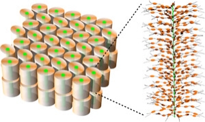
January 25, 2011 — A new form of self-assembling polymer film that bends and stretches when hit by light is pointing the way to a new family of functional materials. This flexing film is the first material to have been made by coaxing complex molecules to form large-scale, highly ordered three dimensional arrays — a discovery that could change the way that many active material are made, from artificial muscles to solar cells.

Nobuhiko Hosono, Takuzo Aida and colleagues at RIKEN Advanced Science Institute in Wako and The University of Tokyo developed the self-assembly protocol. The researchers found that brush-shaped polymers would form an orderly film when hot-pressed between two sheets of Teflon [1].

Click to Enlarge
Figure. The light-responsive film is made up of polymer brushes (right) that have self-assembled into a two-layer, three-dimensional array (left). Reproduced, with permission, from Ref. 1, 2011 American Association for the Advancement of Science.

They made their discovery while studying a polymer in which each side chain, or bristle, of the brush structure incorporates light-responsive azobenzenes: two benzene rings separated by a pair of nitrogen atoms. When hit by UV light, the bond between the nitrogens rearranges, contracting the side chain.

The researchers used this photoisomerization behavior to confirm the remarkable long-range order of the polymer structure. Because the side chains were all aligned, when those at the surface were hit by light they curled up in concert, bending the film. A second beam of light at a different wavelength reversed the isomerization process, and the film relaxed back to its original shape.

The trick to making the material is to heat it between two sheets of Teflon that have been drawn tight in one direction, says Hosono. This tension orients the Teflon sheets’ internal structure along a single axis, which acts as a template for the molten polymer brushes sandwiched in between. The side chains of the polymer brush align with the Teflon, pulling each brush upright. As each polymer brush aligns in the same way, it forms a repeating three-dimensional array (Fig. 1).

Hosono, Aida and colleagues expect the technique to work for other polymer brushes with similar side chains. To improve the artificial muscle-like behavior of their polymer film, Hosono says the team will try cross-linking the polymer side chains. This will prevent the molecular structure from becoming disordered as the polymer repeatedly curls and relaxes over many cycles, giving the muscle a longer lifetime.

The team is already assessing other potential applications. The wide-area three-dimensional molecular ordering of the polymer brush has great potential for building electronic devices, says Hosono. "We now have designed a new type of polymer brush for development of highly efficient thin-layer organic solar cells."

The corresponding author for this highlight is based at the Functional Soft Matter Research Group, RIKEN Advanced Science Institute.

REFERENCE:

1. Hosono, N., Kajitani, T., Fukushima, T., Ito, K., Sasaki, S., Takata, M. & Aida T. Large-area three-dimensional molecular ordering of a polymer brush by one-step processing. Science 330, 808-811 (2010), http://www.sciencemag.org/content/330/6005/808.short

Learn more at http://www.rikenresearch.riken.jp

Follow Small Times on Twitter.com by clicking www.twitter.com/smalltimes. Or join our Facebook group
January 25, 2011 – BUSINESS WIREDiscera Inc., silicon timing technology provider, debuted high-performance MEMS oscillators for networking, server, storage, and video applications. The DSC11XX silicon oscillators are available at accuracies up to 10ppm, and temperature ranges up to 125°C.

The DSC11XX are the highest performance silicon-based oscillators to enter production, with 300 femtosecond RMS phase jitter in CMOS, LVPECL, LVDS, and HCSL output versions, says Discera. "Silicon processes enable a great deal of programmability and flexibility, but until today, they did not provide the highest level of jitter performance, frequency stability, and noise immunity necessary for high-speed communications,” said Bruce Diamond, CEO of Discera.

Independent system-level testing has validated these Silicon MEMS oscillators as exceeding the performance of crystal oscillators for storage and networking applications. GRL testing of the LVPECL DSC1122 found that it surpassed 6G SAS compliance requirements with 59% lower transmitter jitter than the SAS 2.1 specification. UNH Interoperability Labs testing of the DSC1122 found that it surpassed 10 Gigabit Ethernet conformance requirements by delivering transmitter timing jitter 45% lower than the 10GBASE-T specification.

"In our testing of the same production 6G SAS HBA design with both the DSC1122 Silicon MEMS oscillator and a 3rd overtone crystal oscillator, we found that the use of the DSC1122 resulted in equivalent system performance with a bit lower measured transmitter random jitter and total jitter," said Mike Engbretson, chief technology engineer of Granite River Labs. "The results showed the necessity of system-level compliance testing since the crystal oscillator had an even lower RMS phase jitter specification on a component level."

Using Discera’s silicon MEMS technology, the DSC11XX provide excellent jitter while consuming less power and delivering higher frequency stability over a wider temperature ranges than crystal oscillator products. By eliminating the need for quartz crystal or SAW technology, silicon oscillators significantly enhance reliability and accelerate product development. With femtosecond jitter and 10ppm frequency accuracy, DSC11XX oscillators meet the performance demands of high-speed protocols including DisplayPort, Ethernet, Fibre Channel, PON, SAS, and Wi-Gig for signaling rates of 10 Gbps and beyond.

The DSC11XX oscillators are pin-compatible replacements for standard crystal oscillators. Key features include ultra-low phase noise jitter of 300 femtosecond RMS at 156.25 MHz (integrated 200 kHz to 20 MHz), industry-leading frequency accuracy up to 10 ppm across temperature, highest operating temperature range of up to 125°C, and production leadtime of 2 weeks.

Learn more at www.discera.com

Follow Small Times on Twitter.com by clicking www.twitter.com/smalltimes. Or join our Facebook group

January 25, 2011 — LASER COMPONENTS expands its COUNT series of single photon counting modules to include the new COUNTblue devices. These combine low count rates with higher detection efficiencies at shorter wavelengths.

Over 60% of incoming photons can be detected at 405nm, over 65% in the green, while the detection efficiency in the red is typically >50%. The excellent short wavelength performance suits fluorescence measurement and microscopy applications.
 
The COUNTblue features the same robust design as the existing modules and the optional fiber connector allows easy plug&play operation.
 
The product will be featured at Photonics West 2011 (Moscone Center, San Francisco, January 25-27). Learn more at http://www.lasercomponents.com/de-en/product/single-photon-counting-modules-countblue-series/

LASER COMPONENTS develops, manufactures, and sells components and services for the laser and opto-electronics industries. More information is available at www.laser-components.com

Also visit the Nanotech Analytical Equipment Center on ElectroIQ.com

Follow Small Times on Twitter.com by clicking www.twitter.com/smalltimes. Or join our Facebook group

January 24, 2011 — Rambus Inc. (NASDAQ: RMBS), technology licensing company, acquired the lighting and display portfolio of patents and technology from privately held Imagine Designs Inc. The patented innovations include technology for general lighting, LCD backlighting, and microelectromechanical system (MEMS) displays.

"This acquisition complements our portfolio…allowing us to provide a wider range of solutions to our customers for their next-generation LED-based lighting and display products," said Jeff Parker, president of Lighting and Display Technology at Rambus.

Imagine Designs’ founder and principal inventor Brian Richardson will join Rambus as a technical director in the Lighting and Display Technology business. Richardson joins Rambus to continue the development of innovations and solutions for general lighting and displays. In addition, Pete Pappanastos has joined Rambus as a director of strategic development for the Lighting and Display Technology business. Rambus intends to support and further build the customer relationships and momentum that Imagine Designs established in the entertainment, architecture, street light and general lighting markets.

Rambus specializes in the invention and design of architectures focused on enriching the end-user experience of electronic systems. Additional information is available at www.rambus.com.

Follow Small Times on Twitter.com by clicking www.twitter.com/smalltimes. Or join our Facebook group

January 24, 2011 — E M Optomechanical Inc. (EMOpto) developed a new low-cost version of its OPTOPro line of 3D MEMS Optical Profilers for use in testing and characterizing micro-electro-mechanical systems (MEMS) devices.

EMOpto introduced the latest in its line of dynamic 3D MEMS optical profilers, the OPTOPro Model 622-Xe, at less than $20K. It is based on exclusively licensed patented long-working distance interference microscopy technology.

"Feedback from potential customers indicates that tight budgets are preventing them from purchasing our higher priced models and that $20K would be a good price point for an entry level system," says Tom Swann, president of EMOpto. In addition to the Model 622-Xe, customers will have to provide a vibration isolation table, a structure to hold the profiler instrument and a means of holding and positioning the sample to be tested. "We have found that many prospective customers already have these capabilities available in-house," says Swann.

In addition to requiring the customer to furnish some of the system’s components, the low price was achieved by redesigning the mechanical portion of the profiler instrument and trimming the margin on software. "Even at its low price, the Model 622-Xe is a valuable and versatile research tool and it can accommodate a wide range of upgrades" says Swann.

EMOpto’s first generation line of products is intended primarily for use by micro-systems researchers for making real-time dynamic measurements of the micro- and nano-scale motions of MEMS devices and other micro-systems.

The technology behind EMOpto’s line of products was initially developed because there were no commercial optical profilers tailored specifically to the needs of micro-systems researchers. Its key feature is that it allows a long working distance without any sacrifice in measurement resolution. This allows capabilities not possible with other techniques such as allowing space for probes that are needed to attach to micro-system devices and viewing through portholes into vacuum chambers or through device cover glasses. Also read: Detecting failure modes in today’s MEMS

The profiler instrument is controlled by EMOpto’s MEMScript Software that also acquires and analyzes the data collected. This software has several unique features, such as the ability to control micro-system devices, which by nature have moving parts, and making real time measurements of performance. "MEMScriptTM" is a trademark of Sandia Corporation in the United States. Used with the permission of Sandia Corporation, and its licensee E M Optomechanical, Inc.

E M Optomechanical, Inc. was spun-off from Optomec, Inc. in 1998 to provide opto-mechanical engineering, design and fabrication services to the photonics industry. The Company has transitioned to a product oriented Company committed to commercialization of exclusively licensed patented long-working distance interference microscope technology for micro-systems research and development.

Follow Small Times on Twitter.com by clicking www.twitter.com/smalltimes. Or join our Facebook group

UT Dallas nanotechnologists have invented a groundbreaking new technology for producing weavable, knittable, sewable and knottable yarns containing giant amounts of otherwise unspinnable powders. The reseaerchers see applications for the technology in energy storage, energy conversion and energy harvesting. 
Click to Enlarge
Caption: The researchers at the Alan G. MacDiarmid NanoTech Institute at UT Dallas have reported a new technology to embed large amounts of guest powders in nanofibers.

A tiny amount of host carbon nanotube web holds "guest" powders in the corridors of highly conducting scrolls, without altering their performance. With conventional technology, powders are either held together in a yarn using a polymer binder or incorporated on fiber surfaces. Both approaches can restrict powder concentration, powder accessibility for providing yarn functionality, or the strength needed for yarn processing into textiles and subsequent applications.

In the Jan. 7 issue of the journal Science, co-authors working in the Alan G. MacDiarmid NanoTech Institute of UT Dallas describe the use of “bi-scrolling” to solve these problems.

“In this study, we demonstrated the feasibility of using our bi-scrolled yarns for applications ranging from superconducting cables to electronic textiles, batteries and fuel cells,” said Dr. Ray H. Baughman, Robert A. Welch Professor of Chemistry and director of the UT Dallas NanoTech Institute.

Bi-scrolled yarns get their name from the way they are produced: A uniform layer of guest powder is placed on the surface of a carbon nanotube web. This two-layer stack is then twisted into a yarn.

The carbon nanotube webs used for bi-scrolling are not ordinary— they can be lighter than air and stronger pound-per-pound than steel. Four ounces of these webs would cover an acre of land and are about a thousand times thinner than a human hair.

These strong carbon nanotube webs hold together yarns that are mostly powders and can even be machine-washed. The web’s thinness means that hundreds of scroll layers can be included in a bi-scrolled yarn no thicker than a human hair.

The choice of embedded powder determines yarn function. For instance:

  • UT Dallas researchers used yarns imbedded with metal oxide powder to make high-performance lithium ion batteries that can be sewn into fabrics.
  • Bi-scrolled yarns for self-cleaning fabrics were obtained using photocatalytic powder.
  • A powder of nitrogen-containing carbon nanotubes provided highly catalytic yarns for chemical generation of electricity, avoiding the need for expensive platinum catalyst.
  • Using other types of powders, the team made superconducting yarns for potential use in applications ranging from powerful magnets to underground electrical transmission lines.

“UT Dallas’s bi-scrolling technology is rich in application possibilities that go far beyond those we described in Science,” Baughman said. “For instance, our collaborator, professor Seon Jeong Kim of Hanyang University in Korea has already used bi-scrolled yarn to make improved biofuel cells that might eventually be used to power medical implants.”

“I am especially proud of two of our former NanoExplorer high school students, Carter Haines and Stephanie Stoughton, who are undergraduate co-authors of both our article in Science magazine and our internationally filed patent application on bi-scrolling,” Baughman added.

Other co-authors of this article are postdoctoral fellows Dr. Márcio Lima, who is lead author; Dr. Elizabeth Castillo-Martínez, Dr. Javier Carretero-Gonzáles, Dr. Raquel Ovalle-Robles and Dr. Jiyoung Oh; graduate students Xavier Lepró, Mohammad Haque, Neema Rawat, and Vaishnavi Aare; laboratory associate Chihye Lewis; research professors Dr. Shaoli Fang and Dr. Mikhail Kozlov; and Dr. Anvar Zakhidov, professor of physics and associate director of the NanoTech Institute.

Funding for this research was provided by grants from the Air Force, the Air Force Office of Scientific Research, the Office of Naval Research, the National Science Foundation, and the Robert A. Welch Foundation.

January 24, 2011 — Semiconductor Research Corporation (SRC) and researchers from Stanford University have developed a combination of elements that yields a unique nanostructure material for packaging. This advance should allow longer life for semiconductor devices while costing less than current state-of-the-art materials. In addition to chip manufacturers, several other industries could also gain greater product efficiencies from related thermal energy management technology.

Semiconductor manufacturers currently rely on tiny pins or thick solder to bond sections of the semiconductor in order for the device to perform. However, current solder materials tend to degrade and fail due to heat and mechanical stress. To continue the scaling of integrated circuits (ICs), SRC and Stanford have researched materials that provide a high thermal connectivity (comparable to copper) with the flexible compliance of foam. The answer has been created through a nanostructured thermal tape that conducts heat like a metal while allowing the neighboring materials to expand and contract with temperature changes (metals are too stiff to allow this). This ability to reduce chip temperatures while remaining compliant is a key breakthrough for electronic packaging.  

"A big roadblock to increasing the performance of modern chips is hot spots, or millimeter-sized regions of high power generation. This advance in nanostructured materials and methods will allow us to better cool these spots and serves as a key enabler for densification of computational circuitry," said Professor Ken Goodson, lead researcher for SRC at Stanford University. "This can help packaging to withstand the demands of Moore’s Law."

In addressing the challenges of miniaturization, the first line of defense for hot spots is the interface material. Incorporating nearly two decades of advanced research and simulations for problems at the packaging level — much of it funded by SRC — the Stanford team ultimately arrived at their unique combination of binder materials surrounding carbon nanotubes (CNTs). The researchers expect it to facilitate the highest thermal conduction and the most desirable level of elasticity of any known packaging solutions.

"This new thermal nanotape revolutionizes the chip’s heat sink contact," said Jon Candelaria, director of Interconnect and Packaging Sciences at SRC. "Instead of being forced to rely upon the properties of just a single material, this combination gives the integrated circuits industry an opportunity to circumvent severe performance limitations and continue to improve packaging without adding cost."

While the research was funded by members of SRC to enhance computer chips, demand for applications of this kind of thermal interface also is rising in other industries. For instance, several automotive-related companies hope to recover electrical power from hot exhaust gases in cars and trucks using thermoelectric energy converters but reliable interfaces are a problem. Professor Goodson leads a major grant from the National Science Foundation (NSF) Department of Energy Partnership on Thermoelectric Devices for Vehicle Applications, with the goal of transferring the SRC-funded interface work to vehicles.

Patents for the technology are pending. The next step in the research is to license the new methods and materials to advanced thermal-interface companies for application tailoring and commercialization. End users are expected to benefit from the technology by 2014.

For more information and details about the new packaging materials and methods, visit http://pubs.acs.org/doi/abs/10.1021/nl100443x and http://microheat.stanford.edu/publications/A119.pdf.

SRC is a university-research consortium for semiconductors and related technologies that defines industry needs, invests in, and manages the research that gives its members a competitive advantage in the dynamic global marketplace. For more information, visit www.src.org.