Wafer Level Packaging

WAFER LEVEL PACKAGING ARTICLES


Cadence delivers design and analysis flow enhancements for TSMC InFO and CoWoS 3D packaging tech

09/13/2017  Cadence Design Systems, Inc. today announced new capabilities that complete its holistic, integrated design flow for TSMC's advanced wafer-level Integrated Fan-Out (InFO) packaging technology.

Fab equipment spending breaking industry records

09/12/2017  2017 fab equipment spending (new and refurbished) is expected to increase by 37 percent, reaching a new annual spending record of about US$55 billion.

Equipment forecast: $49.4 billion

09/01/2017  In 2018, 7.7 percent growth is expected, resulting in another record-breaking year—totaling $53.2 billion for the global semiconductor equipment market.

The ConFab announces mainstream semiconductor and emerging technologies 2018 conference focus

08/28/2017  The ConFab – an exclusive conference and networking event for semiconductor manufacturing and design executives from leading device makers, OEMs, OSATs, fabs, suppliers and fabless/design companies – announces the 2018 event will be held at THE COSMOPOLITAN of LAS VEGAS on May 20-23.

Semiconductor industry capital spending forecast to jump 20% in 2017

08/22/2017  Samsung remains the “wild card” with regard to 2H17 capital expenditures.

TowerJazz and Tacoma announce a partnership for a new 8-inch fabrication facility in Nanjing, China

08/21/2017  TowerJazz to gain up to 50% of the planned fab loading capacity.

Lam Research takes uniformity control to the edge

08/16/2017  Chipmakers want every part of the wafer to yield good die. Advances in process technologies have just about made this a reality, even as feature dimensions continue to shrink and devices grow more complex.

Mid-year global semiconductor sales up 21% compared to 2016

08/04/2017  Q2 sales are highest on record, 5.8 percent more than previous quarter, 23.7 percent higher than Q2 of last year.

Silicon wafer shortage starts in 2018

07/31/2017  TECHCET's model shows all slack soon gone from supply-chain for both 300mm and 200mm diameter.

Laser debonding for ultrathin and stacked fan out packages

07/27/2017  Fan-out packaging is an established technology for many mobile applications. Whereas early semiconductor packages have been single-chip packages, the continuing trend of expanding the wiring surface to support increased functionality has led to more complex packages, stacked packages, systems inpackageaswellashigh-performancepackages. With this development, fan-out technology is bridging a gap between cost-competitive packaging and high performance.

North American semiconductor equipment industry posts June 2017 billings

07/26/2017  Through the first half of the year, 2017 equipment billings are 50 percent above the same period last year.

Multitest Atlas contactor demonstrates advanced electrical and mechanical performance in WLCSP testing

07/21/2017  Atlas 0.3 mm pitch spring probe validated at customer site.

2017 IEEE IEDM to showcase technology and device breakthroughs in logic, memory, bioelectronics, silicon photonics

07/20/2017  Advances in semiconductor and related devices are driving significant progress in our increasingly digital world, and the place to learn about cutting-edge research in the field is the annual IEEE International Electron Devices Meeting (IEDM), to be held December 2-6, 2017 at the Hilton San Francisco Union Square hotel.

SUNY Poly awarded $720,000 by U.S. Department of Energy for next-generation semiconductor research

07/20/2017  Grant from Energy Department's Advanced Research Projects Agency-Energy supports further development of cutting-edge gallium nitride-based power electronics at SUNY Poly.

Former Micron CEO Mark Durcan to receive semiconductor industry's top honor

07/18/2017  The Semiconductor Industry Association (SIA) announced Mark Durcan, former CEO of Micron Technology, Inc., and a longtime leader in advancing semiconductor technology, has been named the 2017 recipient of SIA's highest honor, the Robert N. Noyce Award.

PLAT4M matures three silicon photonic platforms

07/14/2017  Leti today announced that the European FP7 project PLAT4M has now been completed with results that exceeded expectations.

$49.4B semiconductor equipment forecast: New record, Korea at top

07/12/2017  Worldwide sales of new semiconductor manufacturing equipment are projected to increase 19.8 percent to total $49.4 billion in 2017, marking the first time that the semiconductor equipment market has exceeded the market high of $47.7 billion set in 2000.

SEMI and Solid State Technology announce 2017 “Best of West” Award finalists

06/28/2017  Each year at SEMICON West, the “Best of West” awards are presented by Solid State Technology and SEMI.

It’s time for new innovation

06/20/2017  What if the automotive industry had achieved the incredible pace of innovation as the semiconductor industry during the last 52 years?

How SEMI Standard E175 is saving energy and cutting costs

06/20/2017  Industry experts answer questions about the new standard in a virtual roundtable.


WEBCASTS


Environment, Safety & Health

Date and time TBD

The semiconductor industry is an acknowledged global leader in promoting environmental sustainability in the design, manufacture, and use of its products, as well as the health and safety of its operations and impacts on workers in semiconductor facilities (fabs). We will examine trends and concerns related to emissions, chemical use, energy consumption and worker safety and health.

Sponsored By:

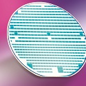
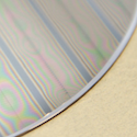
Wafer Processing

Date and time TBD

As the industry moves to 10nm and 7nm nodes, advances in wafer processing – etch, deposition, planarization, implant, cleaning, annealing, epitaxy among others – will be required. Manufacturers are looking for new solutions for sustained strain engineering, FinFETs, FDSOI and multi-gate technologies, 3D NAND, and high mobility transistors.

Sponsored By:

More Webcasts