Table of Contents
Solid State Technology
Year 2001
Issue 3
 | DEPARTMENTS
Think Tank
Shopping Spree
Three engineers, Alfred, Benjamin and Charles, and their wives, Althea, Bernice and Cora (not necessarily in that order), went shopping together while on holiday
Notes From The Floor
Levels of factory automation
Factory automation continues to be a much-debated subject in assembly factories. While advertising campaigns and marketing efforts would have us believe that full automation is a necessity or that only the very best will produce the very best
News
News
Stacked BGA package for wireless communications introduced
New Products
New products
PT Series relays have low profiles and offer 2-, 3- or 4-pole double throw contacts for switching currents up to 12, 10 or 6 amps, respectively
Editorial
Pursuing excellence
There are a few things I can count on hearing when I talk it up with folks in the industry. Among the general niceties people bestow upon us, there is always a mix of good questions, such as "When are you going to cover such-and-such topic?" and "Does this product really work?"
Automotive Perspective
Why reuse?
The term reuse is commonly defined as using something again after some special treatment or processing. Today, it has become socially acceptable to reuse many of the things we have created and mass-produced
|
|
FEATURES
Step By Step
The back-end process: Step 3 - Die attach step by step
In the past, most integrated circuit (IC) packages used wirebonding as the interconnect technology between chip and leadframe
Advanced Tools For Hdi D
Advanced tools for HDI design
Build-up substrates and next-generation design tools Contribute to the miniaturization of electronics
Chip Level Packaging.htm
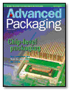
Chip-level packaging
CPU package design must start by addressing form factor. Whether for a high-performance desktop or a high-end workstation/ server, high-speed microprocessor packaging must be designed with the smallest form factor in mind
Two Metal Layer Flex.htm
Two metal layer flex
Typical flex-based packages can be made of pliable base materials, like polyimide or Mylar, onto which conductive metals are deposited and patterned
| |
SUPPLEMENT
Packaging The Next Step
Technology comparisons and the economics of flip chip packaging
The decision to use flip chip packaging is not a simple one. Many equipment, product, and process variables affect the relative merits of flip chip vs. wire bonded packages
Packaging The Next Step
C4 makes way for electroplated bumps
Until recently, controlled collapse chip connection bump technology, developed in the late 1960s, provided a reliable interconnect for high-performance, leading-edge microprocessors
Packaging The Next Step
From dicing to packing: Examining the packaging process
Despite the many advances in assembly manufacturing since the IC was invented, the basic process has not changed significantly
| |
|