Category Archives: Flexible Displays

by Michael A. Fury, Techcet Group

Click to Enlarge July 20, 2011 – About 70 researchers from around the world are gathered this week at The Westin San Francisco for this 7th Organic Microelectronics and Optoelectronics Workshop, co-sponsored by ACS, MRS, IEEE, and IEEE CPMT. The attendee distribution reflects the early research stage of these technologies: 60% university, 20% government labs, and the remainder split between device and materials manufacturers.

John Rogers of UIUC gave the opening talk. Although his group does not deal with organic electronics per se, the applications he targets do indeed overlap quite nicely with those of the organic electronics development programs underway. Semprius, a Rogers Lab spin out, now has an equity investment from Siemens following the successful implementation of a utility scale solar power pilot plant near Tucson using thin flex GaAs cells with optical concentrators. Physiological interfaces to silicon electronics suffer from a severe mismatch in mechanical properties. Flexible silicon on stretchable membranes enables a more highly functional, data-rich interface to the conventional electronics that does not damage living tissue.

Flexible displays using organic TFTs was the topic addressed by Iwao Yagi of Sony. The simplest OLED display circuit is 2T-1C (2 TFT and 1 capacitor) with the single OLED pixel. Different device configurations are used for a flexible design vs. a rollable design to minimize the cumulative mechanical stress on the display components.

Organic Electronics Workshop 2011
Day 1: TFTs, FETs, and a seeing microphone
Day 2: Pushing organic PV performance
Day 3: OLEDs, OTFTs, OPV, and futile resistance

Richard McCreery of the National Institute of Nanotechnology (U. of Alberta, Canada) talked about a robust molecular tunnel junction with high temperature stability (to 150

May 18, 2011 — Conventional ICs are rigid, planar, and brittle. Current flex circuit laminate/metal/laminate structures limit performance and circuits suffer broken interconnects after repeated flexing. The holy grail of flexible electronics would combine the performance of ICs with a form factor that could be stretched, twisted, and conformed to unconventional shapes. David Icke, CEO, MC10 Inc. spoke about flexible electronics in his ConFab Emerging Technologies talk, "Electronics Anywhere: Conformal, Stretchable Electronics Technology & Applications."

Icke discussed flexible silicon nanoribbons that use familar wafer fab processes (think etch, encapsulation) in new IC concepts. "Acordian physics" allow these ribbons to bend and twist without compromising reliability. Conformal polymeric substrates are also in use to reduce stress on the electronics during stretching or twisting, or combinations of movement. The wavy design of Si nanoribbons absorbs strain during excursions (see figure), cushioning the active micro-CMOS "chip" elements. A neutral mechanical plane also limits strain.

The process that Icke described is compatible with conventional foundry equipment and processes, and promises low cost with high yields. >GHz performance is acheivable. The process could ramp for electronics, as well as photovoltaics, LEDs, thin-film batteries, thermoelectric devices, piezoelectrics, sensors, etc.

The electronics can be patterned on unusual substrates (leather, for instance) and shapes (how about a golf ball?). Bending mechanics and interconnect designs are modeled and optimized to accommodate desired configurations and geometries. New flexible electronics can interface with users in revolutionary ways — integrating with the eye or skin, or implanted into the body. Accepted form factors and IC lifetimes, power consumption are not restraints.

Icke shared some ideas for the technology’s application: human-integrated electronics, wearable energy sources, advanced curved imagers, and many other options.

More from the ConFab:


Click to Enlargeby Michael A. Fury, Techcet Group

April 28, 2011 – Day 3 of the MRS Spring 2011 meeting kept me close to my roots, with most of the day spent in the symposium on materials, processes and reliability for advanced interconnects. NVRAM options were my primary distraction from this mission, giving me a reason to move around instead of sitting all day in one place.

I will never understand the point of giving a public presentation at an open forum such as MRS in which every slide is emblazoned with "Confidential Information." If all of your information is this confidential, then it isn’t. My baby engineer training at IBM was apparently well-ingrained, as this misuse of confidentiality labeling still makes me cringe.


(Additional presentation details can be found online on the MRS Spring 2011 abstracts page. The underscored codes at the beginning of papers reviewed below refer to the symposium, session, and paper number.)

InGaAs-on-Si, hardmask showdown, Cu via reliability, flexible electronics

Mitsuru Takenaka of the U. of Tokyo (P5.4) spoke on InGaAs MOS devices on Si. Metal source/drain is required due to limited dopant solubility; Ni has been found to be a good candidate because it forms a good alloy with InGaAs, and Ni can be selectively etched with HCl without affecting the underlying material. Device gate leakage was very low due to the successful removal of excess Ni. Source/drain resistance with Ni is 5× lower than with pn junctions. A fully integrated p Ge and n InGaAs circuit will be presented later this year at the VLSI conference in Kyoto. Examples of III-V photonic devices on Si were also shown.

MRS Spring 2011
Day 1: Lighting the paths for LED materials
Day 2: The III-V future of CMOS, the return of spin-on low-k
Thin-film PV materials under the microscope @ MRS

Olivier Joubert from CNRS in Grenoble, France (O4.1) compared damascene process strategies with metal hard mask to an amorphous carbon hard mask. With the carbon mask, CD control can be an issue due to faceting of the Si-ARC layer during carbon etch. In subsequent etching of the p-SiCOH, control of bowing can be difficult. It is preferred that the low-k material remain hydrophobic to limit uptake of moisture which increases the k value; strategies to ensure this are not well understood. With metal mask, maintaining sidewall profile becomes difficult if the TiN mask is exposed during p-SiCOH etch, due to Ti byproducts interfering. Raising the process temperature from 20°C to 60°C reduces this effect, as the Ti byproducts are more volatile and less likely to interfere. Post-etch treatment with CH4 eliminates the TiF residues that can form during the queue time between plasma etch and hard mask stripping.

Kazuaki Yazawa of UC Santa Cruz (O5.4) used a thermoreflectance microscopy imaging technique to explore copper via chain reliability. Changes in temperature profile over time suggest the ability to determine characteristics of voiding mechanisms and specific locations, but these remain to be further developed.

Ben Schlatka of the U. of Illinois @ Urbana (HH4.4) used an mc10 presentation to illustrate a variety of applications for flexible and stretchable electronics, particularly those coming out of John Rogers’ lab. Semprius, another Rogers spin-out, provides the assembly technology to pick and place the extremely thin Si devices from the host wafer to the target flexible substrate. Stretchable PV is achieved using small individual GaAs cells and buckled interconnects, providing up to 20% stretch. Applications include solar power for a tent, or an unmanned air vehicle in which the wing surface can generate electric power. In partnership with Reebok, an announcement will be made later this year for personal fitness and performance monitoring. Skin-mounted devices are coming for both health care and for human-computer interfacing. The long-term product development for in vivo medical care, which is FDA regulated and requires expensive certification, will be funded by short-term development cycle consumer products.

Memory

Roberto Bez of Micron/Numonyx (Q3.1) provided a status report on advances in NVRAM, primarily phase-change memory (PCM). Ten-year retention is a long time for an old device to sit in the back of the closet, but that’s the design objective. Among the most interesting options are flash, STT-MRAM, RRAM, and PCM. The 45nm 1Gb PCM chip is in volume qualification, using Ge2Sb2Te5. Diffusion effects under operating conditions mean that the local stoichiometry is not uniform, nor is it equivalent to the composition deposited. One possible result is void formation and loss of reliability.

Hongsik Jeong of Samsung (Q3.6) gave his perspective on the status of PCM (which Samsung calls PRAM) as the next NOR technology. They are currently producing a 1Gb 45nm device. The technology is thought to be scalable to 10nm, with the advantage that the operating power scales down with the contact area.

Jong Moon Yoon at KAIST (Q3.8) showed a multilevel PCM scheme using a trilayer PRAM cell array in which each PCM volume has two separate TiN electrodes and two separate crystallization regions, thereby providing three distinct resistance levels per cell. The group was able to fabricate a device with a memory density of 207 Gbit/in2.

Benjamin Kam at IMEC (Q5.1) described an organic ferroelectric FET memory device based on a low-leakage P(VDF-TRFE) layer. The programming voltage can be limited to ±15V by using a P(VDF-TRFE) thickness of 200nm. Leakage currents of 10-9 A/mm2 at 1 MV/cm are exceptionally low.

Philipp Sebastian at TU Dresden (Q5.6) described an organic ReRAM device based on C60 buckyballs. The device is read at +1V, written at +4V and erased at -4V, with an on/off ratio of 10. R/W time is 50μsec, durability is 104 cycles, and the retention time of weeks is dependent on the interim readout frequency.

Mikhail Dronov of the General Physics Institute in Moscow (Q5.7) showed a new memory device concept based on an organic MEH-PPV layer mixed with 5μm particles of Zn or Fe-Ni alloy. RON/ROFF is 106, with switching times of 100ns to turn on, 1μs to turn off. Durability was tested to 104 cycles with no degradation. Retention >3 months is believed to be due to filament formation. Addition of a photoactive compound to the organic layer allows the device to be turned on by light, with retention comparable to electrical switching, but this cannot be explained by filament formation.

Low-k dielectrics

Sven Zimmermann of Fraunhofer ENAS (O4.2) proposed a process flow to reduce damage in ultralow-k (ULK) integration. Modifications of the etch chemistry can reduce the k damage by promoting CH2 species and maintaining hydrophobicity. HMDS was chosen as a k repair medium by immersion at 150°C followed by 2min UV exposure, which reacts with the near-surface damage but not the bulk.

Theo Frot from IBM (O4.3) proposed a ULK-friendly integration scheme called post-porosity plasma protection, or P4. The k=2.0 material is based on Et-OCS. After dielectric formation, pores are filled with a separate polymer material to protect the porosity structure during etch. The secondary polymer is removed following etch at 400°C in N2. Electrical results will be reported at IITC next month (May 2011).

Griselda Bonilla of IBM Watson (O5.1) addressed several of the key reliability issues associated with low-k dielectric materials. The primary parameters monitored are EM, TDDB and CPI reliability. Defects do not scale, and the majority of TDDB failure mechanisms become worse with ULK materials. JUSE drops 2× with each generation and may constitute a fundamental electromigration scaling limit as the copper mass continues to decrease. ULK energy release rate can be 30% higher than low-k, providing another driving force for mechanical reliability problems.

Barrier materials

Expressing his relief to be back in a region that allows for a normal life — though some of our more conservative citizens might question whether San Francisco actually qualifies — Junichi Koike of Tohoku U. in Sendai, Japan (O6.1) spoke on the attributes of CVD MnO as a copper barrier layer. The barrier forms as an embedded layer in the dielectric, but the barrier-dielectric interface can form an undesirable high-k dielectric; for example, MnO-TEOS can be as high as k=10.7. The CVD MnO was deposited from Mn(EtCp)2 to a thickness of 3-4nm with good step coverage even at the via bottom. MnO adhesion was good at a deposition temperature up to 300°C; above 400°C the precursor pyrolizes, increasing carbon content and decreasing adhesion. Dielectric breakdown was 4MV/cm at 550°C, indicating good barrier function.

Shaoning Yao from IBM (O6.2) continued the Mn barrier theme with a CuMn alloy seed layer to improve electromigration results. This is used in conjunction with the conventional Ta/TaN barrier, not as a replacement for it, and was successfully integrated at 32nm. Line depletion failure improves by 10×-25×. Further a non-gouging liner (TaN/Ta/CuMn at the via bottom) performed 2× better than a gouging liner (no TaN at the via bottom).

Neda Dalili of the U. of Alberta (O6.3) took a look at amorphous TaN as a copper diffusion barrier. During anneal at 500°C-800°C, TaSi forms in samples of TaN on Si when there is copper present on top of TaN, but not when there is no Cu present. With Cu, the barrier integrity is preserved to 700°C, but at 800°C the TaN barrier fails and Cu3Si forms. Amorphous TaN crystallizes to Ta2N above 500°C, and the volume displacement defects allow Cu diffusion to occur.

Ryan Birringer at Stanford (O5.2) studied the adhesion of barrier materials to copper and related properties. Impurities in the barrier films tend to promote stress-induced void formation, which in turn leads to surface fracture and adhesion degradation. HKMG systems were also studied.

Deposition

Taehoon Cheon at Yeungnam U. (Korea) (O6.7) has an ALD process for RuAlO barrier films that enable direct Cu plating without a seed layer. Ru is not suitable by itself as a Cu barrier due to its polycrystalline columnar grain structure. This ternary Ru alloy is one of several that have been proposed. Films are formed at 225°C using Ru(EtCp)2 and Al(CH3)3 ALD deposition super cycles up to a ratio of 40:5. Excellent conformality was demonstrated in an AR=32 trench. Direct plating of Cu without a seed was shown with good adhesion.

Sanghyuk Choi at Yeungnam U. (O6.8) spoke about the deposition and plating properties of ALD Ru barrier using the zero valence Ru precursor described in Cheon’s talk. Growth rate was 0.08nm/cycle with negligible incubation cycles of ~9, indicating the rapid nucleation of Ru. The deposition is self-limiting, indicating a surface reaction and not thermal decomposition. Adhesion on Ta was comparable to PVD Ru. Resistivity was 15μΩcm with a polycrystalline columnar grain structure.


Michael A. Fury, Ph.D, is senior technology analyst at Techcet Group, LLC, P.O. Box 29, Del Mar, CA 92014; e-mail [email protected].

April 18, 2011 — Henkel, an adhesives, sealants and surface treatments provider, and Holst Centre, an open-innovation initiative by imec and TNO, partnered in flexible electronics development. Henkel will contribute an adhesives knowledge base to the Holst Centre’s shared research programs on large-area flexible organic photovoltaics (OPV), organic light emitting diode (OLED) lighting and signage, and other areas.

Adhesives with functional properties like electrical conductivity or moisture barrier protection have great potential in future electronics applications, such as heterogeneous integration of silicon and plastic electronics or lamination and interconnection of functional foils to form working devices such as flexible solar cells (OPV), OLED lighting devices, or flexible displays. Henkel plans to bring many of its technologies to these applications, drawing on expertise in electronics adhesives, pressure sensitive adhesives, and more.

Within its program on "Integration technologies for flexible systems," Holst Centre built a track record of generic technologies that can decrease the design complexity of flexible electronic devices and therefore the future cost of fabrication. Henkel adds a new field of expertise to the existing eco-system of industrial partners in the shared research program. Adhesives can potentially impact a large number of the investigated processes.

The partnership allows Henkel to further evaluate and develop its optically clear, electrically conductive and moisture barrier technologies, among others, on actual devices, beyond isolated material samples. This makes it more efficient to assess the market readiness of new developments. "This partnership brings for Henkel a great opportunity to evaluate adhesives in real (organic) electronic devices, allows us to create and test new adhesive concepts with technical experts in flexible electronics and key future end-users," said Thomas Kostka, R&D Manager at Henkel, adding that they expect to bring innovative fit-for-use technologies significantly faster to the market.

Holst Centre is an independent open-innovation R&D centre that develops generic technologies for Wireless Autonomous Sensor Technologies and for Flexible Electronics.

Subscribe to Solid State Technology/Advanced Packaging.

Follow Advanced Packaging on Twitter.com by clicking www.twitter.com/advpackaging. Or join our Facebook group

April 7, 2011 – BUSINESS WIRE — CCID Consulting Co. Ltd. (HKSE: 08235), China-based ICT research and management consulting firm, released its 2010-2011 Survey on China’s OLED Industry Development at Consumer Electronics Market China 2011 this March in Suzhou.

OLED technology

The CCID survey indicates that the small-sized organic light emitting diode (OLED) technology has become mature and is entering the mobile phone market in a fast manner. OLED featuring self-luminosity, ultra thinness, fast response, wide viewing angle and low power consumption has helped the OLED-screen mobile phones gain great popularity. OLED has initially established its position as the core of the third-generation display. With technical advancement and breakthroughs in the mass production of large-sized OLED, the industry will embrace a new era of larger-sized OLED. Industry analyst firm NanoMarkets released "OLED Lighting Markets Asia-2011," which says the market opportunities in Asia for OLED lighting will generate $2.1 billion by 2016.

iPhone played a significant role in driving the popularity of large-sized smart phones and enabled the debut of OLED screens in the market. The active OLED (AMOLED), in particular, is heavily dependent on high-end mobile phones and larger-sized application consumption. The sales revenue of AMOLED has continued to grow since it beat PMOLED in 2009.

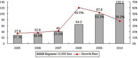
The market has been expanding with the technical advancement and application upgrades. According to CCID Consulting statistics, supported by demand for mobile phones and application products including MP3/MP4, OLED display screen market has been seeing a rapid growth since 2005. In 2010, China’s OLED shipment reached 1.352 million sets, up 38.2% year-on-year, which was attributable to both the growing market demand and the increase in the manufacturers’ capacities.

Currently, most of the OLED panel manufacturers are located in Japan, South Korea and Taiwan. NanoMarkets’ report states that Japan will dominate the OLED lighting business through 2014 despite lingering issues from the earthquake and tsunami. Japanese consumers have greeted LED lighting enthusiastically and will do the same as OLED lighting gets onto retail shelves. Meanwhile, Japanese firms are taking up key positions in every part of the worldwide OLED lighting supply chain from design and manufacture through to wholesale distribution. Sales of OLED lighting in Japan are expected to reach $1.1 billion by 2016.

Korea is early in its embrace of OLED lighting and NanoMarkets predicts sales of only reach $230 million by 2016. But, the influence of both Samsung and LG cannot be understated as both have made a strong commitment to OLED lighting and NanoMarkets notes how Samsung’s strong international brand has brought OLED displays into the mainstream. The firm sees great potential for OLED lighting from Samsung’s involvement in the technology.

With the launches of Samsung SDI’s world’s first AMOLED panel, Sony 11" AMOLED TV and LG’s 15"AMOLED TV, the manufacturers in Japan, South Korea and Taiwan have strengthened their competitiveness in OLED market and also gained a favorable position in the AMOLED market, says CCID. Besides, other manufacturers including LG Display, CMEL, TMD and Samsung Electronics have also accelerated their AMOLED technology development.

Based on its long-term research on the status and development trends of the OLED industry, CCID Consulting forecasts that in the three years to come, the demand for OLED panels will see a rapid growth as the demand for consumer electronics continues to expand.

Click to Enlarge

Figure. Shipment and growth rate of China’s OLED industry, 2005-2010 Source: CCID Consulting, February 2011

China

With the support of China’s Ministry of Industry and Information Technology (MIIT), OLED R&D in mainland China has achieved a number of breakthroughs. In October 2008, Visionox, established by Tsinghua University, completed the first OLED mass production line in Kunshan City of eastern China’s Jiangsu Province, and started the mass production of small-sized OLED display screens.

At the end of 2010, small-sized OLED manufacturers in mainland China included Visionox, Shanwei Truly, Sichuan CCO and IRICO. China’s first AMOLED medium experimental line has been commissioned in Kunshan, which acquired all the required production techniques at the end of 2010. Shanghai Tianma and IRICO, respectively, are in process of constructing G4.5 AMOLED production lines, with debut of mass production expected within 2011, while BOE and Sichuan CCO are also actively engaged in AMOLED R&D projects.

OLED requires planning to integrate resources, facilitate innovations, direct various enterprises to enter the OLED industry chain and grant financial support to achieve sustainable development of the industry in China. Although the addressable market for OLED lighting in China is limited, NanoMarkets expects the Chinese OLED lighting market to reach $420 million by 2016. OLED lighting markets and manufacturing in China are expected to benefit from current Chinese industrial policy which emphasizes the need to develop high-tech industries to serve the domestic Chinese market.

Governmental support continued in 2010 on the basis of the Planning on Adjusting and Revitalizing the Electronic Information Industry issued in 2009, including the MIIT’s special funds for the electronic information industry and industrial demonstration bases, as well as Ministry of Finance’s tax policies on new display manufacturers’ imported materials.

So far, China has not yet formed its OLED industry chain, without any domestic full-set OLED manufacturing equipment producers and with key equipment and full-set equipment technologies dominated by the Japanese, South Korean and European enterprises. It lacks raw materials including indium tin oxide (ITO) glass, photoresist, desiccant and UV curing adhesives for packaging. Meanwhile, China’s development of AMOLED techniques is facing great difficulty due to the backward TFT technologies, inferior panel techniques and inadequate management.

Other weak points of China’s OLED industry include: limited financing channels due to the immaturity of China’s capital market; inadequate basic research, industry standards, and resouces integration; and development and management talents are badly needed.

As China did not enter the CRT and LCD arena at the early stage and failed to develop its core technologies and competitiveness, the country could only join the industry’s low-profit assembling and testing sections with its advantages of cheap labor force and strong OEM capacities. However, the emergence of OLED provides a great opportunity for China’s display industry.

China is both a major producer of the world’s consumer electronics and it is the world’s largest OLED application market. In this market, more than 45% of the IT products are related with display devices; the output of mobile phones in mainland China accounts for over 50% of the global total; the output of MP3/MP4 in mainland China accounts for over 90% of the global output; and the output of other consumer electronics in mainland China accounts for over 50% of the global total. As the cost further goes down and the capacity continues to grow, the OLED panels will be more widely used in other consumer electronics. For instance, the domestic brand Lenovo’s LePhone has adopted a AMOLED screen, marking the debut of OLED on domestic mobile phones.

Driver ICs

Many companies are engaged in the design and production of OLED driver ICs worldwide. The OLED active driver panel has limitations such as high prices and poor compatibility with silicon materials and organic materials, which has become a bottleneck slowing the development of the global OLED industry. China depends on driver IC imports and lags behind other countries in large-sized and color screen technologies due to its outdated equipment and limited investment. In addition, the industry’s key patents are all held by foreign companies. For example, Kodak and Idemitsu Kosan hold the fundamental patents of small molecule OLED materials and structures; CDT and DuPont hold the fundamental patents of polymer PLED materials and structures; SANYO, Sharp, SEL and Eldis, South Korean Samsung, LG and Industrial Technology Research Institute hold certain core patents of active drivers.

CCID Consulting Co. Ltd. is a Chinese consulting firm directly affiliated to China Center for Information Industry Development (CCID Group). Learn more at
http://en.ccidconsulting.com

NanoMarkets tracks and analyzes emerging market opportunities in energy and electronics markets created by developments in advanced materials. Visit www.nanomarkets.net  

Subscribe to Solid State Technology/Advanced Packaging.

Follow Solid State Technology on Twitter.com via editors Pete Singer, twitter.com/PetesTweetsPW and Debra Vogler, twitter.com/dvogler_PV_semi.

Or join our Facebook group

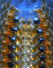
January 13, 2011 — The black teeth of an Eastern beaded chiton, a sea mollusk, are used for scraping algae from rocks. They are capped with one of the hardest biominerals known, a nanocomposite of magnetite and chitin-based fibers.

Click to EnlargeTeeth and bone are important and complex structures in humans and other animals, but little is actually known about their chemical structure at the atomic scale. What exactly gives them their renowned toughness, hardness and strength? How do organisms control the synthesis of these advanced functional composites?

The interface between the organic and inorganic materials plays a large role in controlling properties and structure, said Derk Joester, senior author of the paper. How do organisms make and control these materials? We need to understand this architecture on the nanoscale level to design new materials intelligently. Otherwise we really have no idea what is going on.

Joester is the Morris E. Fine Junior Professor in Materials and Manufacturing at the McCormick School of Engineering and Applied Science. Lyle Gordon, a doctoral student in Joester’s lab, is the other author of the paper.

Using a highly sophisticated atomic-scale imaging tool on the sea creature’s tooth, the Northwestern University researchers have peeled away some of the mystery of organic/inorganic interfaces that are at the heart of tooth and bone structure. They are the first to produce a three-dimensional map of the location and identity of millions of individual atoms in the complex hybrid material that allows the animal to literally chew rock.

Joester and Gordon imaged teeth of the chiton, a tiny marine mollusk, because much is known about the biomineralization process. The chiton lives in the sea and feeds on algae found on rocks. It continually makes new rows of teeth — one a day — to replace mature but worn teeth; in conveyor-belt fashion, the older teeth move down the creature’s tongue-like radula toward the mouth where it feeds.

Chiton teeth resemble human teeth in that they have a hard and tough outer layer — equivalent to our enamel — and a softer core. Instead of enamel, the rock-chewing chitons use magnetite, a very hard iron oxide, which gives their teeth a black luster.

Demonstrating that atom-probe tomography (APT) can be used to interrogate such materials opens up the possibility of tracking fluoride in teeth and cancer and osteoporosis drugs in bone (at previously inaccessible length scales). The detailed knowledge of organic/inorganic interfaces also will help scientists rationally design useful new materials — flexible electronics, polymers and nanocomposite materials, such as organic photovoltaics — that combine the best properties of organic and inorganic materials.

The researchers set out to find the organic fibers they knew to be an important part of the tooth’s structure, buried in the tough outer layer of the tooth, made of magnetite. Their quantitative mapping of the tooth shows that the carbon-based fibers, each 5 to 10 nanometers in diameter, also contained either sodium or magnesium ions. Joester and Gordon are the first to have direct proof of the location, dimension and chemical composition of organic fibers inside the mineral.

They were surprised by the chemical heterogeneity of the fibers, which hints at how organisms modulate chemistry at the nanoscale. Joester and Gordon are anxious to learn more about how the organic fibers interface with the inorganic minerals, which is key to understanding hybrid materials.

The tooth’s toughness comes from this mix of organic and inorganic materials and the interfaces between them, Joester said. While this is, in principle, well known, we may have overlooked how subtle changes in the chemical makeup of nanoscale interfaces may play a role in, for instance, bone formation or the diffusion of fluoride into tooth enamel. In this regard, atom-probe tomography has the potential to revolutionize current understanding.

Atom-probe tomography produces an atom-by-atom, 3D reconstruction of a sample with sub-nanometer resolution. But many in the field didn’t think APT would work to analyze a material made up of organic and inorganic parts. Northwestern’s David Seidman, a leader in the field, uses APT to study metals. The school also has two of the few APT instruments in the US. Seidman, Walter P. Murphy Professor of Materials Science and Engineering, encouraged Joester to take the risk and use APT to study biological architectures. The scientists also were able to exchange ideas with the engineers developing 3D atom-probe instruments at CAMECA, a scientific instrumentation company in nearby Madison, WI.

The researchers extracted micron-sized samples from the leading edge of the chiton tooth. Using a focused ion beam (FIB) tool at the Northwestern University Atomic and Nanoscale Characterization Experimental Center core facility, these samples were fashioned into very sharp tips (<20nm across). The process is reminiscent of sharpening a pencil, with a supercharged stream of gallium ions.

The APT technique applies an extremely high electric field to the sample; atoms on the surface ionize, fly off, and hit an imaging detector. The atoms are stripped off atom-by-atom and layer-by-layer. Computer methods then are used to calculate the original location of the atoms, producing a 3D map or tomogram of millions of atoms within the sample.

The results are published today by the journal Nature. The title of the paper is Nanoscale chemical tomography of buried organicinorganic interfaces in the chiton tooth. Read the abstract here

Joester and Gordon now are studying the tooth enamel of a vertebrate and plan to apply APT to bone, which is also made of organic and inorganic parts, to learn more about its nanoscale structure.

The National Science Foundation and the Canadian National Sciences and Engineering Research Council supported the research.

Courtesy of Megan Fellman, Northwestern University. Copyright 2011 States News Service

Follow Small Times on Twitter.com by clicking www.twitter.com/smalltimes. Or join our Facebook group

(January 5, 2011) — SmartKem Ltd, developer of novel printable semiconductor materials for flexible electronics, announced that the Welsh Assembly Government has awarded the company £335,000 in funding to further develop its flexible printed electronics solutions.

Based in Denbighshire, Wales, SmartKem is a high-technology enterprise delivering and generating a novel range of organic semiconductor molecules and ink formulations compatible with printed electronic processes. This is an inexpensive, low weight, low energy, alternative to silicon semiconductors and can be used to print organic circuits and devices onto thin flexible substrates such as plastics and paper.

Initial Venture Capital funding from Finance Wales allowed SmartKem to relocate to the world class OpTIC Technium facility in North Wales and accelerate its growth in the flexible printed electronics industry.

SmartKem has now received further recognition as an innovative company and has been awarded a grant of £335,000 from the Welsh Assembly Government. The grant will help advance the company’s vision to deliver world-leading printable semiconductor technology to the microelectronics industry for applications such as electronic displays, thin-film RFID, smart sensors and printed logic circuits. 

The Welsh Assembly Government is committed to encouraging businesses to invest in R&D to stimulate innovation, which is a key driver of productivity and economic growth. Ieuan Wyn Jones, Minister for the Economy and Transport, said the Assembly Government’s strategy, "Economic Renewal: a new direction," focused support on businesses like SmartKem working in key sectors with high growth potential.

"We are extremely keen to increase the amount of innovation and R&D carried out in Wales, particularly in our key sectors, and pleased to hear how our support is helping SmartKem. It is also welcome news to hear that SmartKem was singled out for a gold award in the Venturefest 2010 Best of British Innovation Award, which recognized the company as one of the year’s most exciting technology businesses."

Steve Kelly, CEO SmartKem, comments: "We are delighted to be awarded with this grant and extremely pleased that the Welsh Assembly Government has decided to support SmartKem at such an exciting time. This is a huge boost for the company and allows us to continue our breakthrough research and development projects and further penetrate the rapidly growing printed electronics industry."

SmartKem is focusing on high-performance/high-value organic semiconductor materials that can be printed to form electronic circuits onto lightweight, rugged and low-cost polymer films. For more information on SmartKem, visit www.smartkem.com.

(November 30, 2010 – Marketwire) — The FlexTech Alliance, focused on developing the electronic display and the flexible, printed electronics industry supply chain, has awarded a contract to Cambridge NanoTech to develop a high-speed atomic layer deposition (ALD) system. When completed, the system will enable the manufacture of large-area and flexible substrates for use in organic electronics, solar cells, biomedical devices, and displays.

The high-speed ALD system is targeted to operate at the high volumes necessary for commercial roll-to-roll practices. ALD enables perfect, conformal, ultra-thin films that are scalable to large-area substrates. ALD simultaneously offers excellent thickness uniformity, film density, step coverage, interface quality, and low temperature processing, making ALD beneficial for both roll-to-roll flexible substrates and rigid substrates.

"We are honored to be selected by the FlexTech Alliance to industrialize ALD and bring it to the forefront of thin film technology," said Ray Ritter, COO of Cambridge NanoTech. "This exciting, new technology will advance the way flexible electronics, displays and other next-generation consumer devices are fabricated."

"The FlexTech Alliance supports the mission to help build a commercially viable industry around flexible and printed electronics," said Michael Ciesinski, CEO of FlexTech Alliance. "The high-speed ALD system that Cambridge NanoTech will develop with this award stands to play a key role in commercializing the flexible electronics market."

To accelerate the ALD process, the engineering team at Cambridge NanoTech is focusing on cycle time reduction by means of a high speed precursor delivery and extraction mechanism. The beta system will be installed at the Flexible Display Center at Arizona State University in 2012. In addition to designing and building the high-speed ALD system, Cambridge NanoTech is developing film processes that are applicable to electronics and display manufacturers.

Visit Cambridge NanoTech at Booth #622 at the Material Research Society meeting at the Hynes Convention Center in Boston, MA.

The FlexTech Alliance fosters the growth, profitability and success of the electronic display and the flexible, printed electronics supply chain. Learn more at www.flextech.org.

Cambridge NanoTech delivers Atomic Layer Deposition (ALD) systems capable of depositing ultra-thin films that are used in a wide variety of research and industrial applications. To learn more about Cambridge NanoTech, visit www.cambridgenanotech.com.

(November 17, 2010 – Marketwire) — The Flexible Display Center (FDC) at Arizona State University announced that AU Optronics (AUO) has become an industry partner of the FDC. The two companies will collaborate on the development of mixed oxide thin film transistors (TFTs) to accelerate the commercial availability of active-matrix organic light-emitting diode (AMOLED) flexible displays.

AMOLED displays have already started to gain market traction in conventional glass displays for applications such as smart phones because of the crisp, vibrant and rich colors they deliver. The FDC-AUO partnership will focus on bringing the benefits of AMOLED displays, including full-color, full-motion video, to flexible substrates. Also read, "LED substrates and singulation discussion with Jan Vardaman"

"We see tremendous potential in partnering with the FDC to advance the development of flexible AMOLEDs," said Yong-Hong Lu, VP of AUO Technology Center. "The FDC has significant experience in adapting standard flat panel display manufacturing technologies for use with flexible substrates, which is a critical aspect of being able to bring flexible AMOLEDs to market. Working with the FDC offers us an opportunity to advance leading-edge display technologies for flexible substrates and participate in the development of viable approaches to commercialization."

AUO and the FDC will work in active partnership with dedicated engineering teams to advance mixed oxide transistor technology and the handling capabilities of conventional flat panel display (FPD) manufacturing processes to accommodate the thin, plastic substrates used for flexible displays. Mixed oxide TFTs offer a better ability to drive currents and improve the lifetime and stability of transistors used for OLED displays.

"As one of the leading FPD manufacturers in the world, AUO brings significant expertise in AMOLED display technology and manufacturing," said Nicholas Colaneri, director of the Flexible Display Center at Arizona State University. "This partnership will allow us to combine AUO’s manufacturing strength with the FDC’s superior approach to handling plastic materials in a conventional flat panel manufacturing environment. Working with AUO further extends our strategy of fostering innovation with leading industrial firms by taking advantage of the Center’s unique public, private and military partnership to accelerate the development of advanced technologies."

The FDC is a government/industry/academia partnership for advancing full-color flexible display technology and fostering development of a manufacturing ecosystem to support the rapidly growing market for flexible electronic displays. More information on the FDC can be found at http://flexdisplay.asu.edu/.

AU Optronics Corp. (AUO) provides thin film transistor liquid crystal display panels (TFT-LCD). For more information, visit www.AUO.com.

Subscribe to Solid State Technology/Advanced Packaging.

Follow Advanced Packaging on Twitter.com by clicking www.twitter.com/advpackaging. Or join our Facebook group

(October 11, 2010) — The 6th edition of the Global Plastic Electronics Conference & Exhibition takes place October 19-21 at Messe Dresden in Dresden, Germany and for the first time it will be held together with the SEMICON Europa 2010. This year’s Physics Noble Laureate, Dr. Kostya Novoselov, will speak about graphene at the show.

Dr. Kostya Novoselov will present, "Graphene: Materials in the Flatland." His talk will be given within the Plastic Electronics Conference on Thursday, October 21 in the plenary hall of Messe Dresden. Novoselov and co-researcher Andre Geim won the Nobel Prize in Physics just days ago for their work on graphene nano material.

This week in Dresden will become an international focus point for new developments in the electronic industries. About 8000 professionals from science and industry are expected to attend the combined event.

The Plastic Electronics Conference program will include speakers from Philips Lighting, Osram, Merck, Samsung, Cambridge University, Stanford University, and more. There will be more than 100 lectures from prominent experts recognized for their outstanding achievements in this field.

The six topics of the conference are: Organic Electronics, Displays, Organic Photovoltaics, Lighting, Smart Integrated Systems, and Novel System Approaches. The adjacent exhibition offers the opportunity to see demonstrators, services and products as well as network.

The Plastic Electronic Conference & Exhibition 2010 and the SEMICON Europa 2010 are combined at the "Converging Electronics Week." Within this dual-hosted and dually organized event, there will be enterprise-tours to local businesses and expert workshops on organic electronics and semiconductor technology.

Dresden is the largest European locations for organic electronics and one of the top locations in the world. More than 850 specialists are working in one of Saxony’s fastest growing high-tech industries today. Saxony’s close network of universities, research-facilities and businesses, encourages excellent knowledge transfer lab-to-fab. The Free State of Saxony will have an opening reception on October 19 for all regular registered attendees of the conference.

OES — Organic Electronics Saxony e.V. represents the interests of the largest European cluster of organic semiconductor. The network combines local, midsize companies as well as some of the most important, global players working in the field of organic electronic research and development in Saxony. OES supports specifically the internal know-how-transfer in R&D and offers a platform to boost the existing global market position successfully and efficiently. www.oes-net.de

The Plastic Electronics Foundation is a not-for-profit organization whose main objective is to promote the technology of printable, organic based flexible electronics into marketable applications and products worldwide. For more information please contact [email protected]

SEMICON Europa is a leading European exposition for microelectronics manufacturing with an expanding focus on growing markets including MEMS, printed/flexible electronics, solid state lighting, and related technologies. www.semiconeuropa.org

Follow Small Times on Twitter.com by clicking www.twitter.com/smalltimes. Or join our Facebook group