Category Archives: Materials and Equipment

(August 9, 2010) — The High Density Packaging User Group International Inc. (HDP User Group), a global non-profit cooperative research and development organization for the electronics manufacturing industries, will start a new project group focusing on optical electronics. At this time the projects is in definition stage, and open to all member and non-member companies interested in the focus area.

Optoelectronics, which uses light pulses rather than electrical pulses to transmit signals, offers many potential benefits to next generation electronic products, such as higher speed, less interference, and lower power consumption. HDP User Group is excited about the new project and expects several important topics to be created from it. Read more about optoelectronics at www.optoIQ.com.

The HDP User Group’s Optical Interconnect project aims to alleviate intra-cabinet interconnect bottlenecks envisaged in Terabit-scale (Tbps) systems, as data rates are reaching 15-25 Gigabit-per-second (Gbps) per lane, by connecting electronic devices with optical paths. The project is developing optical interconnect architectures that can respond to capacity and energy efficiency needs of future high-speed systems, e.g. high performance computers, servers, routers and switches.

Although the primary focus is on data and telecommunication segments, the aim is to provide a generic technology platform for a wide range of applications, e.g. avionics. The project addresses the key challenges prohibiting implementation of optical technology for inter- and intra-card links including robust optical connections, optical design and simulation practices, compliance of optical materials and components with the manufacturing and assembly processes, and lack of system-level performance and reliability data. In the first stage, fully optical chip-to-chip data links will be demonstrated with optical backplanes containing integrated polymer waveguides. Key building blocks needed to realize the optical backplane, including novel system and link architectures, optoelectronic packaging, optical channels, optical interfaces and CMOS I/O circuitry – will be studied with experiments. "To exploit the full promise of the optical technology, we need to re-evaluate system architectures to benefit from the capabilities of optical interconnects, and we need some more new innovations and breakthroughs in the key technologies involved in the optical technology, especially optical printed circuit boards and optical backplane connectors," says Shaoyong Xiang, of Huawei Technologies, and a member of the project.

The system evaluation metrics include cost, size, power efficiency, electrical interface, latency and bit-error-ratio (BER). Passive alignment, low-cost packaging, automated assembly and testing are targeted for cost viability. For pursuing the long-term vision of an optical communications system with embedded optical waveguides on cards and backplanes connecting on-chip silicon photonic interconnects, the project aims to demonstrate technical viability and cost competiveness of optics with practical steps. This means that near-term solutions are a combination of fiber and waveguide technologies. The second step is to demonstrate optics within an application, for instance, within a multiprocessor architecture. "We expect adaptation of optical backplanes within 4-5 years. Yet, before commercial viability, cost must be comparable to copper, and technical issues, especially at connections, must be solved. Also, the supply chain needs to exist with confidence of the new materials, their compatibility, performance and reliability. And, we need standards around the technology. Ability to combine efforts through industry collaboration gives possibilities to reach major technical breakthroughs, pave the way for wider acceptance and acceleration of commercializing the technology," says Marika Immonen, Manager of Optical Interconnects Research and Development at TTM Meadville and leader of the project.

"The members of HDP User Group are working together to understand the benefits and solve the technical hurdles to the implementation of this important technology. A coordinated effort such as this is necessary to quickly bring the full benefits of Optoelectronics into widespread use," noted Marshall Andrews, executive director of HDP User Group. The field of optoelectronics is so diverse with numerous technical issues that the Project Team has already created subgroups of the main opto project in the areas of devices, waveguides, architecture and standards recommendations. As more areas of interest are identified the project team is prepared to add additional subgroups. HDP User Group welcomes the input and participation of any organization interested in the field of optoelectronics.

Jack Fisher, who is involved with several international technology roadmaps, says that the time is right for this project. Optoelectronics continues to show up on the technology roadmap horizon and this particular project seems to fit a need of the industry. Jack is a veteran printed circuit board technologist and is HDP User Group’s project facilitator for this activity. Jack has been involved in other optoelectronic projects in the past.

For further information on the new project visit http://hdpug.org/content/optoelectronics. HDP User Group is a global research and development organization based in Scottsdale AZ, dedicated to "reducing the costs and risks for the Electronics Manufacturing industry when using advanced electronic packaging and assembly." For more information, visit www.hdpug.org

Read more about optoelectronics in Advanced Packaging:

Back-side illumination, wafer-scale optics drive 2×-5× jump in CMOS image sensor performance
Ultrathin silicon that enables back-side illumination (BSI), and integrated wafer-level optics are bringing sharply improved performance, lower costs, and smaller size, driving CMOS image sensors into more and more markets—and these technologies may soon impact other IC manufacturing as well, say Jerôme Baron, Yole Développement.
Read it here: http://www.electroiq.com/index/display/semiconductors-article-display/1735263071/articles/solid-state-technology/volume-53/issue-7/departments/technology-news/back-side-illumination.html

(August 9, 2010) — A Europe-wide consortium has taken up the challenge of making a significant impact on the power consumption of telecommunications and data networks, which are estimated to consume as much as 3% of European electricity. Five partner organizations have come together in the BIANCHO project (BIsmide And Nitride Components for High temperature Operation), a 3-year research and development initiative supported by €2.190 million through the EU Framework 7 program.

The project will develop new semiconductor materials to allow lasers and other photonic components to become more energy efficient and also more tolerant of high operating temperatures. This power reduction is vital as optical communication systems are becoming the principal way to deliver ever-increasing data-rich broadband services to homes and businesses.

Follow Solid State Technology on Twitter.com via editors Pete Singer, twitter.com/PetesTweetsPW and Debra Vogler, twitter.com/dvogler_PV_semi. Or join our Facebook group

Many current photonic components for telecommunications applications have major intrinsic losses, with around 80% of the electrical power used by a laser chip being emitted as waste heat, for example. The presence of this waste heat necessitates the use of thermo-electric coolers and an air-conditioned environment in order to control the device temperature, cascading the energy requirements by more than an order of magnitude.

The energy losses are mainly due to a process known as Auger recombination, a consequence of the band structure of the semiconductor materials used in making components such as semiconductor lasers and optical amplifiers. Over many years, incremental approaches have sought to reduce the consequent inefficiencies without addressing their fundamental cause. BIANCHO proposes a radical change of approach: to eliminate Auger recombination by manipulating the electronic band structure of the semiconductor materials through the use of novel dilute bismide and dilute nitride alloys of Gallium Arsenide and Indium Phosphide. This will allow the creation of more efficient and temperature tolerant photonic devices which could operate without the power-hungry cooling equipment that today’s networks demand.

The project brings together five leading European partners with complementary expertise in epitaxy, structural characterization of materials, device physics, band structure modelling, advanced device fabrication, packaging and commercialization. Coordinated by the Tyndall National Institute (Ireland), internationally recognized for its strength in semiconductor band structure modelling, the other academic partners are Philipps Universitaet Marburg (Germany) focussing on material growth and characterization; Semiconductor Research Institute (Lithuania) responsible for the design, manufacture and characterization of bismide-based epitaxial structures; the University of Surrey (UK) who contribute unique characterisation facilities and modelling expertise. Commercialization of the project results will be led by CIP Technologies (UK) an organization with a long history of applied photonics innovation, particularly in the telecommunications sector.

Further information:

Tyndall National Institute – www.tyndall.ie/ptg
Contact: Mary O’Regan ([email protected]) Tyndall National Institute is the largest ICT-related research institute in Ireland. Tyndall covers a broad range of research capabilities in the areas of photonics, electronics and nanotechnology as well as related technological areas such as the interface between the Life Sciences and ICT.

Philipps University Marburg – www.uni-marburg.de/wzmw/strl
Contact: Professor Kerstin Volz ([email protected])
The Material Sciences Center (WZMW) of Philipps University Marburg (UNIMAR) is an interdisciplinary research centre founded in 1988. It encompasses groups from the departments of physics, chemistry and pharmacy and is engaged with research as well as with teaching in the respective departments. The structure and technology research laboratory (http://www.uni-marburg.de/wzmw/strl) deals mainly with the growth and characterisation as well as processing of and the application of III-V semiconductor heterostructures.

University of Surrey – www.surrey.ac.uk
The University of Surrey is one of the UK’s leading professional, scientific and technological universities with a world class research profile and a reputation for excellence in teaching and research.

Center for Physical Sciences and Technology, Semiconductor Physics Institute
Contact: Professor Arunas Krotkus ([email protected]) Semiconductor Physics Institute (http://www.pfi.lt/index_e.html ) is the largest research institute dealing with semiconductor technology, material and device investigations in Lithuania and in the Baltic countries.

CIP Technologies – www.ciphotonics.com
Contact: Michael Robertson ([email protected])
CIP Technologies is the trading name of The Centre for Integrated Photonics Ltd, a world-renowned developer of advanced photonic hybrid integrated circuits and InP-based opto-electronic chips, devices, arrays and modules for the communications, defence and renewable energy markets.

(August 5, 2010) — Vycom consolidated its fire-safe product offerings under the Flametec family of clean room and semiconductor materials. Flametec fire-safe materials are specially formulated to exceed fire compliances for polymers in semiconductor, clean room, and other applications. Flametec is used for a variety of applications including tools, wet benches, cabinetry and furniture.  With excellent workability, the chemically resistant materials are easy to fabricate and form.

The products:

Flametec Clean Room PVC-C: designed to be the most economical FM4910-rated material choice while maintaining superior chemical resistance. It suits use in construction of wet benches, process tools, and clean room furniture and cabinetry. This product is a true CPVC material with no plasticizers added and is available in a range of thicknesses.

Flametec CP-7D Flame Retardant Polypropylene: a proprietary formulation of flame retardant polypropylene designed for wet process tools, furniture and cabinetry construction and fume and exhaust hoods. The consistent formula, superior surface aesthetics and light weight FM4910 material make it suitable for clean room applications

Flametec KytecR PVDF: an ultra pure fluoropolymer well suited for harsh chemical, thermal and ultraviolet environments, Kytec is resistant to most acids, bases and organic solvents. It is used in semiconductor, petrochemical and nuclear industries. Kytec targets wet process tools, plenum and chemical tanks, chemical containment, pulp and paper, petrochemical, metallurgical and pharmaceutical applications. With excellent mechanical strength and stiffness as well as abrasion and creep resistance, Kytec is FM 4910 and FDA compliant.

Flametec CP-5 Flame Retardant Polypropylene: formulated to meet the SEMIS93 and UL 94 V-0 specification for fire safety in clean room applications. CP-5 provides a more competitive alternative when a factory mutual listing is not required.  It is used for laminar air flow stations, clean room accessories, biological safety cabinets and fume hood. With superior impact strength, CP-5 has a consistent formulation and is available in a variety of thicknesses as well as oversized sheets.

Vycom, a division of CPG International, offers products, capabilities, and inventory for all Olefin and PVC. For more information, visit http://www.vycomplastics.com.

Follow Solid State Technology on Twitter.com via editors Pete Singer, twitter.com/PetesTweetsPW and Debra Vogler, twitter.com/dvogler_PV_semi. Or join our Facebook group

(August 4, 2010) — Jeremy Lug, Dynamics Research Corporation Metrigraphics Division, goes over what you need to know to design bio-compatible medical electronics on time, on budget, and with FDA approval to sell. A lot of medical device engineering is tradeoffs between materials, processes, labor, and other factors.

Engineers in all industries strive to push the technology edge forward into uncharted territories. In the flexible circuit industry, the majority of circuits have existed comfortably for many years within the line and space size range of 4mils (~100µm) and higher without the need to undergo a serious size reduction.

While large segments of the market continue to operate there, electronic equipment and technology advances have created the need for flexible circuits with expanded requirements and line and space sizes in the micron range. 

 
Figure 1. Square traces are circuits with lines and spaces in the 5-10µm range that enable small, flexible circuits to be used in a variety of implantable applications.

Transitioning from one size range to the next still represents a tremendous challenge for materials, processes, and manufacturability. The introduction of aspect ratio optimization and material/process incompatibilities could present new problems not encountered to-date by designers. However, these challenges can be addressed at the same time or serially depending on the resources available, and the window of opportunity. One way to address the incompatibility challenge is introducing square traces into the manufacturing process. Square traces are circuits with lines and spaces that can be used in a variety of implantable applications. They facilitate the transition process from size ranges (Fig. 1).

Biocompatibility

Biocompatibility means that the device, with its intended micro components, either resides in vitro (entirely within the body) or in close contact with the body (on the surface of the skins or subcutaneously). In some cases, it means to be used for a brief period of time within the body, but not left there.

From a medical device standpoint, specific devices — such as IV tubing and some types of medical sensors — require a level of biocompatibility so they can be used in the medical field. Essentially, devices that need to be biocompatible are ones that, either directly or indirectly, come in contact with bodily fluids or tissue, creating a need for biomedically safe materials and processes that can function within the human body.

The FDA has requirements for each of these applications, and the designer needs to be mindful of such requirements, selecting the level of compatibility then ensuring approval and operational acceptance.

 
Figure 2. Round coils have lines and spaces in the 5-10µm range that can be used for antennas to transmit and receive signals or as inductors to transmit signals and power from outside the body to inside.

Not all devices will need to be biocompatible, but processes will have to change to be able to produce circuits reliably for the medical field. One way to ensure biomedical compatibility is inserting round coils that can be used for antennas to transmit and receive signals or as inductors to transmit signals and power from outside the body to inside. (Fig. 2).

Material selection

Materials currently used in high-volume circuit applications may not be compatible for micro-medical devices. Biocompatibility is a major requirement for medical devices if they are not completely encapsulated. Biomedical material selection will be difficult at times due to the smaller population of materials that meet the requirements, and materials that can be adapted into current manufacturing processes. 

Material quality will also need to improve as defects that are acceptable at larger line-widths will be rejected at smaller line-widths. Inclusion of foreign material, voids, air bubbles and other visible defects impact customer acceptance of a biocompatible product.

Biocompatible materials will dictate the materials and processes by which circuits are fabricated and engineers will often have to make compromises as prototype designs are evaluated and produced. Many times these processes are at odds with low-cost volume manufacturing and design to cost decisions about correct material selection will have to be carefully made.  

Eventually, as the global volume of micro flexible circuitry increases, the material volume and diversity will increase as material cost decreases. There will continue to be new material advances and discoveries as companies practice continuous process improvement, and grow their inventory of intellectual property (IP). Emerging companies with new ideas and aggressive marketing techniques will push technology along in their quest for market share.

Processing

Different combinations of processes and materials can also aid in producing high-volume micro-circuits where larger size standard technology has often been constrained by process limitations precluding the small sizes. Research into alternate processes — some from the semiconductor industry and some from other previously unrelated fields — can help define the future of the miniature flexible circuitry. In many ways, the development of current micro-circuits came out of developments in the semiconductor industry.

Follow Small Times on Twitter.com by clicking www.twitter.com/smalltimes. Or join our Facebook group

Manufacturing engineers will be able to optimize the touch labor in the production line by using a variety of process development tools such as a design of experiments (DoE), and/or other similar design packages. Processes can be tailored to existing equipment, and the workplace layout optimized for product flow. 

To expedite product development, some products can be prototyped with commonly used materials, and then, while testing is in process, the materials can be changed out for biocompatible materials. These commonly used materials are more readily available and more cost-effective than the new state-of-the-art biocompatibles. This could lower the cost of the initial prototypes, and separate the two challenges: miniaturization and biocompatibility. Of course, once the design goes to the FDA for approval, it must use the final design, process and materials to secure approval.

Prototype circuits are typically developed at a high cost. The real challenge is taking the defined requirements and making the circuits manufacturable in high volumes, but at low cost. At times, these challenges can be solved with automation, while other cases require modifying the approach to achieve equivalent results. Understanding targets ensures the designer moves in the right direction from the onset of the project. No one wants to find out late in the game that the perfect design cannot be produced at a price that the market will bear. Working with the prototype vendor early on to identify design cost drivers is critical to success.

Costs

Precious metals will be used for many medical devices to make them biocompatible, leading to higher direct material costs. These costs will have to be offset with lower production costs, or result in higher end prices. However, with micro circuits, the percentage of high-cost material content is generally small, thus the total impact on price can be minimal. With an understanding of design needs, materials can often be mixed to better match cost targets.

Devices such as these could command a higher price, but it is easier to gain market share when the price is the same or lower than the currently used device. There will be trade-offs depending on the volume being produced — like the degree of touch labor versus automation or capital investment. With high volume potentials, investments in capital can help take labor cost out of the part and reduce its overall cost to produce.

Suppliers and partners

The search for material and equipment suppliers for this high end market is increasingly difficult. Today’s economy is changing the typical customer. Where once relationships were characterized by suppliers and receivers, the industry is witnessing customers becoming partners.

Partners can work together to optimize design, processes, materials, and equipment to meet specific requirements. These affiliations can result in a higher degree of quality, lower material cost, and higher profit margin for both partners as well as boost throughput and on-time deliveries as well as create production flows that reduce or eliminate the need for large inventories of product or materials.

Conclusion

Production of micro-miniature flexible circuits continues to increase. Miniaturization is still on the steep slope of the learning curve, so the market could see many advances in the near future.  Reductions in unit cost are a daily challenge, and are happening with advances in materials and optimization of processes using the latest manufacturing principles of lean, six-sigma, and statistical process control (SPC). 

Biocompatibility may be a new requirement to some areas of industry, while an alternative requirement to others. Each portion will continue to advance in its own direction, taking advantage of new materials and technology. Maintaining the high degree of quality as different processes are introduced into the high-volume manufacturing environment is achievable with cooperation, dedication, and a drive for innovation. The next challenge is just around the corner.

Jeremy Lug received his bachelor’s degree in microelectronic engineering from Rochester Institute of Technology and is the manager of new product development at Dynamics Research Corporation, Metrigraphics Division, 50 Concord Street, Wilmington, MA 01887; (978) 658-6100; [email protected].

Read more about medical and life sciences technology

(August 3, 2010) — A newly discovered nanomaterial could improve healthcare devices by increasing energy storage, help realize implantable microchips, or make better drugs. Scientists at the University of Texas have created silicon nanoneedles with modulated porosity. The nanoporous needles are flexible, semiconductors, biodegradable, and have a surface one hundred times larger that of solid nanowires.

Figure 1. A side view of a forest of bicolor nanoneedles. A central low porosity segment is green and two siding high porosity segments are red. An ultrathin porous wire crosses the picture sideways, in yellow.

These unique properties of the nanowires will provide a higher energy density when used as large surface anodes in lithium batteries; constitute the active elements of bioresorbable, flexible microchips for subcutaneous implants; or protect drugs while in the body and release them in a controlled manner to improve their therapeutic effect.

Figure 2. Bicolor nanoneedles seen from an angle. The high porosity segment is red and low porosity segment is green. The grass-like flexibility of the nanowires allows the tips to join.

“We have indicated that the novel combination of nanoscale dimensions of the needles with their flexibility, ability to conduct electricity, degrade in the body and have the ‘surface of a tennis court’ on the tip of your thumb is crucial to develop lithium batteries that can store more energy, produce integrated circuits (ICs) that can be implanted in the body, and deliver drugs more efficiently. All these components are necessary to design better healthcare devices” says Mauro Ferrari, chair of the NanoMedicine and Biomedical Engineering Department.

Figure 3. A forest of evenly spaced cylindrical nanoneedles. The diameter is 100nm and allows piercing of cell membrane without harming the cells.

Conducted by researchers at the department of NanoMedicine and Biomedical Engineering at the University of Texas, the study reports the use of a new, rapid and inexpensive etch mechanism that uses silver nanoparticles to form nanoneedles from silicon. The needles are synthesized in a solution of hydrogen peroxide. The porosity is controlled along the length of the needle by simply changing the concentration of peroxide over time. The porosity causes the needles to biodegrade in a predictable way over time, and gives them a surface 120 times larger than that of corresponding solid wires while maintaining the semiconductor and crystalline nature.

The study was supported by the National Institutes of Health (NIH), the Defense Advanced Research Projects Agency (DARPA) and the state of Texas.

Follow Small Times on Twitter.com by clicking www.twitter.com/smalltimes. Or join our Facebook group

“We can control the size and shape of the porous structure using the same technology currently used to make computer microchips, and we are doing it to make needles with a tip smaller than 100nm. This will allow us to penetrate directly within many cells at once and delivery drugs very specifically inside them without killing the cell,” says Ciro Chiappini, leading author of the study and researcher at the University of Texas at Austin.

The researchers have also shown that they can control the dissolution of the needles over several days and thus determine the life of the resulting implantable device. They can also control the color of the needles through porosity to design nanoneedles barcodes with codebars of different colors. Since porous silicon is not harmful to cells these barcodes can be used to tag cells and chemical reactions. “The barcodes are a very efficient system to identify cells in the natural environment without altering their functions, and we will use them to track movement of multiple cells at once. That is what I’m working on right now” says Jean Raymond Fakhoury, another author of the study.

The university research is the cover story in July 25th Advanced Functional Materials, http://www3.interscience.wiley.com/journal/123537708/abstract

(August 2, 2010) — Japan Marketing Survey Co. Ltd. (JMS) will publish "Outlook of thermal interface material market 2010) this week, with data on the semiconductor package thermal management market size by application, thermal interface material types’ market shares, and more.

Follow Advanced Packaging on Twitter.com by clicking www.twitter.com/advpackaging. Or join our Facebook group

The thermal interface material (TIM) market is broken out by semiconductor package application and type. Market size forecasts go from 2009 to 2014. manufacturers’ shares (by application and material type) are calculated based on 2009 data. Applications include PCs, consumer electronics, infrastructure, automotive devices, and others. Types include solid TIMs, fluids, and phase change materials (PCM)

In the thermal filler market, market sizes (2009-2014) and manufacturers’ shares are given for alumina and boron nitride.

To order the report, visit JMS at http://www.jms21.co.jp/english.ver/report/syoseki/2010report/TIM_2010.htm

Read more about thermal interface materials here: http://www.electroiq.com/index/packaging/ap-materials/thermal-management.html

Read more about electronics manufacturing here: http://www.electroiq.com/index.html

(August 2, 2010) — Carl Zeiss SMT debuted an integrated gas injection system on the ORION Plus Helium Ion Microscope. The gas injector reportedly delivers superior nanofabrication, deposition and etch.

Tungsten Pillar deposited with Helium Ion Beam (7700nm tall and 45nm diameter) (Photo: Business Wire)

The combination of a sub-nanometer (<0.35nm) probe of inert gas ions with a small interaction volume at the sample surface enables highly precise induction chemistries. The resulting structures have extremely small dimensions and high profile fidelity.

Dr. Paul Alkemade at the Kavli Institute of Nanoscience, Delft University of Technology, is one of the early researchers in helium ion-induced deposition and etching. According to Dr. Alkemade, "The optimum instrument for nanofabrication requires both high spatial resolution and high deposition efficiency. Fortunately, the Helium ion beam on the ORION Plus instrument provides resolution for deposition that is even better than that achieved by a scanning electron microscope (SEM). In addition, the Helium ion beam provides deposition efficiencies that are very similar to those achieved with a heavy ion (Ga) focused ion beam (FIB) instrument. With the integration of a Gas Injection System, the ORION Helium Ion Microscope is proving to be the right instrument for nanofabrication research." Read more about nano production equipment here: 

Follow Small Times on Twitter.com by clicking www.twitter.com/smalltimes. Or join our Facebook group

http://www.electroiq.com/index/nanotech-mems/tools-equipment.html

The controls for the Gas Injection System (GIS) are integrated through the ORION Plus system software. The GIS unit contains three crucibles capable of delivering metal and insulator deposition and insulator etch chemistries. User programmable recipes can be created and recalled allowing for complex deposition and etch processes. The Gas Injection System on the Orion Plus creates a powerful and flexible platform enabling state-of-the-art nanofabrication applications.

Carl Zeiss SMT AG comprises the Semiconductor Technology Group of the Carl Zeiss Group. Carl Zeiss SMT manufactures lithography optics and light, electron and ion-optical inspection, analysis and measuring systems. Further information is available at www.smt.zeiss.com

Other Carl Zeiss SMT product news:

Carl Zeiss debuts SEM with enhanced resolution in the low kv region 

Carl Zeiss delivers "complete" optics for production EUV

Zeiss debuts "correlative microscopy" elements

Zeiss touts particle analysis add-on for SEMs

Carl Zeiss adds nanopatterning engine for FIB/SEMs

Zeiss adds variable pressure to Sigma FE-SEMs 

Executive Overview

We developed low-temperature, defect-free Cu-Cu direct bonding processes with high interfacial adhesion energies. The quantitative analyses of the interfacial adhesion energies and seam voids of Cu-Cu bonds performed with varying process parameters showed that bonding temperature and post-bond annealing have the most significant influence on bond properties. By optimizing experimental parameters, we could achieve, even with a short bonding time, sufficient interfacial adhesion energies (≥5 J/m2 for the subsequent processes such as grinding) with no interfacial seam voids. Post-bond annealing performed at 250-300°C drastically improves the interfacial adhesion energy.

Bioh Kim, Thorsten Matthias, Erkan Cakmak, EV Group, Inc., Tempe, AZ USA; Eun-Jung Jang, Jae-Won Kim, Young-Bae Park, Andong National University, Andong, Korea

Through-silicon via (TSV) technology represents a system-level integration of planar devices that are stacked and interconnected in the z-direction. TSV integration enables the smallest form factor and highest performance due to the shortest and most plentiful interconnects between chips. Due mainly to the thermal budget of CMOS devices, the bonding processes compatible with TSV-interconnected CMOS wafers are limited only to direct oxide bonding, metal bonding (Cu-Cu or Cu-solder-Cu), adhesive bonding and various hybrids of those methods.

Among all, Cu-Cu direct bonding has several advantages over other bonding methods, which include lower electrical resistivity, better electromigration (EM) resistance and significantly reduced interconnect RC delay [1-2]. However, the reliable Cu-Cu bonding for most industrial applications comes only from high temperature, high pressure and long process time mainly because of its tendency to form a native oxide which deleterioiusly impacts device reliability. Presently, high process temperature is one of the major bottlenecks of Cu-Cu direct bonding because it can negatively influence device reliability and manufacturing yield. Typically, the industrial Cu-Cu bonding process is performed at ≥ 400°C, requiring over an hour of the total process time.

The ultimate goal of this work is to develop the low temperature Cu-Cu bonding process while maintaining strong bonding energies. As the first step, we focused on understanding the impact of varying process parameters, such as bonding temperature, chemical pre-treatment, pre-bond annealing and post-bond annealing, on the interfacial properties (voids and seams) and subsequent adhesion energies.

Quantitative analyses of Cu-Cu direct bonds

The quantitative analyses of interfacial adhesion energies and interfacial seam voids of Cu-Cu bonds were performed with varying process parameters, where the 4-point bending method was used to measure interfacial adhesion energies and a focused ion beam (FIB) was used to examine interfacial seam voids.

Click to Enlarge
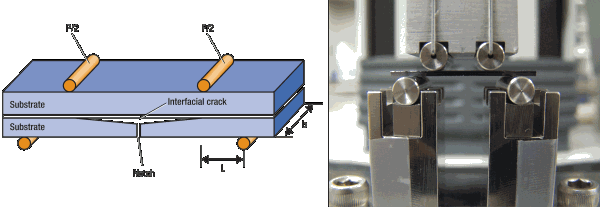
Figure 1. Sample structure for 4-point bending test.

Figure 1 illustrates the schematic of the sample for the 4-point bending experiment. The sample was placed between four load pins. A notch with the depth of 450µm was made on the bottom Si sample with a diamond blade to uniformly initiate the crack propagation during the bending test. The 4-point bending test is based on the fracture mechanics and used to calculate the interfacial adhesion energy between thin films, by measuring the energy release rate (G) which is required for a crack to propagate at the inner homogeneous material [3]. The sample has two elastic materials in a sandwich structure and the adhesion energy was measured during crack propagation at a constant moment, where a crack propagates along the weakest interface in multi-layers [4].

The interfacial adhesion energy, G (J/m2), was calculated using the following expression

Click to Enlarge

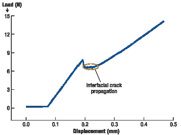
where v is Poisson’s ratio for an elastic material (Si wafer: 0.28), E is the elastic modulus of the elastic material (Si wafer: 130GPa), b and h are the width (3mm) and thickness of the specimen (500µm), respectively, P is the measured load, L is the distance between the inner and the outer loading points (5mm) and M is the moment defined as PL/2. In this experiment, the load cell was 20N, the loading speed was 0.08µm/s, and the distance between pins was 5mm. Figure 2 shows an example of the load-displacement curve of the Cu bonding layer from the 4-point bending test. The interfacial adhesion energy was obtained by using the plateau load in this graph.

Click to Enlarge
Figure 2. Load-displacement curve for Cu-Cu layer from 4-point bending test.

Experimental parameters

We used 100mm diameter blanket wafers with the thickness of 500µm. All the bonding experiments were performed using an EVG520 bonder at 25kN, 10-3Torr and N2 atmosphere. The vacuum level was initially maintained at 10-6Torr, but dropped to 10-3Torr when N2 was purged before the bonding process started.

Process parameters evaluated in this work include

• bonding temperature; 300, 350 and 400°C,

• chemical pre-treatments with a diluted acetic acid (80 vol.%); 1, 5, 10 and 15min,

• pre-bond annealing; 100 and 200°C for 15min at forming gas atmosphere, and

• post-bond annealing; 200, 250 and 300°C for 60min at N2 atmosphere.

Experimental results and discussion

Among all the tested conditions, bonding temperature and post-bond annealing showed the most significant influence on the interfacial adhesion energy and seam void formation. In comparison, the impacts of chemical pre-treatment and pre-bond annealing with the aforementioned conditions were much smaller. By adjusting those two experimental parameters, we could achieve, even with a short bonding time (30min), sufficient interfacial adhesion energies (≥ 5J/m2) with no interfacial voids. Post-bond processes such as grinding require typically at least 5J/m2 of the interfacial adhesion energy [5].

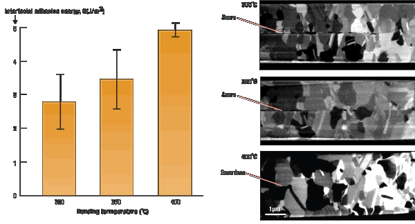
Bonding temperature effect. Wafers with 1.5µm thick, sputter-deposited Cu film on Si(100)/SiO2/Ta(25nm) were used for this experiment. Neither pre-bond surface treatment nor post-bond annealing was applied to samples. The pressure applied to the stack was 25kN and the bonding time was 30min, which is shorter than typical Cu-Cu bonding time (≥ 60min). With increasing bonding temperature, the interfacial bonding energy increased as illustrated in Fig. 3a. With the bonding temperature of 400°C, the minimal adhesion energy (5 J/m2) required for the post-bonding processes such as grinding was achieved. The original bond interface tended to disappear with increasing bonding temperature (Fig. 3b), which led to higher interfacial adhesion energy. All the fracture occurred through the Cu-Cu interfaces.

Click to Enlarge
Figure 3. Interfacial properties as a function of bonding temperature; (a) interfacial adhesion energy and (b) microstructures of samples.

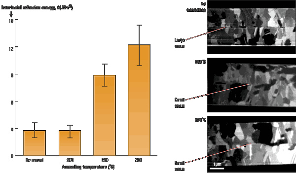
Post-bond annealing effect. All bonding tests were performed at 300°C and 25kN for 30min without any chemical pre-treatment or pre-bond annealing. Those samples were post-bond annealed at 200, 250 and 300°C, respectively, at N2 atmosphere for 60min. Figure 4a compares the microstructures of the samples annealed at different temperatures. In the case when post-bond annealing was not applied, the original interface or large seam was observed together with small voids because this bonding test was done at a low temperature with a short process time. With applying post-bond annealing at 200°C, no improvement in the interfacial properties was observed. After annealing either at 250°C or at 300°C, it was clearly observed that the interfacial seams between two layers decreased significantly. This means the post-bond annealing at 250-300°C can help Cu diffuse through the bond interface even when bonding is done at a low temperature (e.g., 300°C in this experiment). As illustrated in Fig. 4b, a decrease in the interfacial seam size resulted in higher bond strengths with increasing annealing temperature. In all cases the fracture occurred through the Cu-Cu interfaces.

Click to Enlarge
Figure 4. Interfacial properties as a function of post-bond annealing temperature; (a) interfacial adhesion energy and (b) microstructures of samples.

Post-bond annealing conditions evaluated in this experiment were not strong enough to fully drive the recrystallization reaction at the interface between two Cu films, but sufficient to drastically improve the interfacial properties. Further optimization of subsequent post-bond annealing conditions is ongoing to lower Cu-Cu bonding temperature under 200°C. If a long process time for post-bond annealing is concerned for volume production, a batch annealing process can be suggested after bonding wafers.

Conclusion

Cu-Cu thermo-compression bonding facilitates fine-pitch, high density stacking of various devices resulting in lower electrical resistance and higher mechanical strength. With varying process conditions, the quantitative analysis of the interfacial adhesion energy of Cu-Cu thermo-compression bonds was performed using the 4-point bending test and the interfacial properties such as voids and seams were also examined with FIB to correlate the relationship between the interfacial properties and resulting adhesion energies. The process conditions evaluated in this work include bonding temperature, chemical pre-treatment, pre-bond annealing and post-bond annealing.

Among all, bonding temperature and post-bond annealing have the most significant influence on bond properties. By optimizing experimental parameters, we could achieve, even with a short bonding time (30min), sufficient interfacial adhesion energies (≥5J/m2) with no interfacial voids. With increasing bonding temperature (300, 350 and 400°C), the interfacial adhesion energy increases and the original bond interface tends to disappear. The post-bond annealing performed at 250°C or 300°C under N2 atmosphere for 60min, even though thermo-compression bonding was done at a low temperature (300°C), drastically improves the interfacial adhesion energy (8.87–12.17J/m2) by more than three times.

Acknowledgments

The following were co-authors of this paper: Seungmin Hyun and Hak-Joo Lee of the Korea Institute of Machinery & Materials, Daejeon, Korea.

References

  1. A. Fan, A. Rahman, R. Reif, "Copper Wafer Bonding," Electrochem. and Solid-State Lett., 2, 534 (1999).
  2. S. I. Kim, C. W. Lee, "Nitrogen Impurity Effects of W–B–C–N Quaternary Thin-film for Diffusion Barrier for Cu Metallization," J. Korean Phys. Soc., 50, 489 (2007).
  3. R. Shaviv, S. Toham, P. Woytowitz, "Optimizing the Precision of the Four-point Bend Test for the Measurement of Thin-film Adhesion,, Microelectronic. Eng., 82, 99 (2005).
  4. H. Zhenyu, Z. Suo, X. Guanghai, H. Jun, J. H. Prevost, N. Sukumar, "Initiation and arrest of an interfacial crack in a four-point bend test," Eng. Fracture Mech., 72, 2584 (2005).
  5. R. Tadepalli, Ph. D. Thesis, "Characterization and Requirements for Cu-Cu Bonds for Three-dimensional Integrated Circuits," Massachusetts Institute of Technology (2007).

Contact author:

Bioh Kim is Global Business Development Manager at EV Group, Inc., 7700 S. River Parkway, Tempe, AZ 85284, USA; ph.: 480-294-9342; email  [email protected].

More Solid State Technology Current Issue Articles
More Solid State Technology Archives Issue Articles

(July 30, 2010) — Package on package (PoP) stacking makes use of the vertical space available on electronics printed circuit boards (PCBs). It increases density, fitting more silicon into the same footprint. However, package stacking can be difficult, as fine pitches require placement accuracy, and taller stacks generally face reliability issues, especially if the stack is reflowed improperly. So where should PoP stacking take place?

Take this short survey and tell us what you think, and why: http://www.surveymonkey.com/s/packageonpackage

Read about other 3D packaging technologies and read Advanced Packaging’s online feature about PoP rework from BEST Inc.

(July 29, 2010) — Graphene, a sheet of pure carbon and a possible replacement for silicon-based semiconductors, has been found to have a unique property that could make it even more suitable for future electronic devices. When subjected to a 3-point stretch, graphene sprouts nanobubbles with electrons moving as if subjected to a strong magnetic field. The discovery was made by physicists at the University of California, Berkeley, and the Lawrence Berkeley National Laboratory (LBNL).

Figure. A scanning tunneling microscope image of a single layer of graphene on platinum with four nanobubbles at the graphene-platinum border and one in the patch interior. The inset shows a high-resolution image of a graphene nanobubble and its distorted honeycomb lattice due to strain in the bubble. (Source: Crommie lab, UC Berkeley)

Specifically, the electrons within each nanobubble segregate into quantized energy levels instead of occupying energy bands, as in unstrained graphene. The energy levels are identical to those that an electron would occupy if it were moving in circles in a very strong magnetic field, as high as 300 tesla, which is bigger than any laboratory can produce except in brief explosions, said Michael Crommie, professor of physics at UC Berkeley and a faculty researcher at LBNL. Magnetic resonance imagers use magnets less than 10 tesla, while the Earth’s magnetic field at ground level is 31 microtesla.

"This gives us a new handle on how to control how electrons move in graphene, and thus to control graphene’s electronic properties, through strain," Crommie said. "By controlling where the electrons bunch up and at what energy, you could cause them to move more easily or less easily through graphene, in effect, controlling their conductivity, optical or microwave properties. Control of electron movement is the most essential part of any electronic device."

Crommie and colleagues report the discovery in the July 30 issue of the journal Science

Aside from the engineering implications of the discovery, Crommie is eager to use this unusual property of graphene to explore how electrons behave in fields that until now have been unobtainable in the laboratory.

"When you crank up a magnetic field you start seeing very interesting behavior because the electrons spin in tiny circles," he said. "This effect gives us a new way to induce this behavior, even in the absence of an actual magnetic field."

Among the unusual behaviors observed of electrons in strong magnetic fields are the quantum Hall effect and the fractional quantum Hall effect, where at low temperatures electrons also fall into quantized energy levels.

The new effect was discovered by accident when a UC Berkeley postdoctoral researcher and several students in Crommie’s lab grew graphene on the surface of a platinum crystal. Graphene is a one atom-thick sheet of carbon atoms arranged in a hexagonal pattern, like chicken wire. When grown on platinum, the carbon atoms do not perfectly line up with the metal surface’s triangular crystal structure, which creates a strain pattern in the graphene as if it were being pulled from three different directions.

The strain produces small, raised triangular graphene bubbles 4 to 10 nanometers across in which the electrons occupy discrete energy levels rather than the broad, continuous range of energies allowed by the band structure of unstrained graphene. This new electronic behavior was detected spectroscopically by scanning tunneling microscopy. These so-called Landau levels are reminiscent of the quantized energy levels of electrons in the simple Bohr model of the atom, Crommie said.

The appearance of a pseudomagnetic field in response to strain in graphene was first predicted for carbon nanotubes in 1997 by Charles Kane and Eugene Mele of the University of Pennsylvania. Nanotubes are a rolled up form of graphene. Within the last year, however, Francisco Guinea of the Instituto de Ciencia de Materiales de Madrid in Spain, Mikhael Katsnelson of Radboud University of Nijmegen, the Netherlands, and A. K. Geim of the University of Manchester, England predicted what they termed a pseudo quantum Hall effect in strained graphene. This is the very quantization that Crommie’s research group has experimentally observed. Boston University physicist Antonio Castro Neto, who was visiting Crommie’s laboratory at the time of the discovery, immediately recognized the implications of the data, and subsequent experiments confirmed that it reflected the pseudo quantum Hall effect predicted earlier.

"Theorists often latch onto an idea and explore it theoretically even before the experiments are done, and sometimes they come up with predictions that seem a little crazy at first. What is so exciting now is that we have data that shows these ideas are not so crazy," Crommie said. "The observation of these giant pseudomagnetic fields opens the door to room-temperature ‘straintronics,’ the idea of using mechanical deformations in graphene to engineer its behavior for different electronic device applications."
Crommie noted that the "pseudomagnetic fields" inside the nanobubbles are so high that the energy levels are separated by hundreds of millivolts, much higher than room temperature. Thus, thermal noise would not interfere with this effect in graphene even at room temperature. The nanobubble experiments performed in Crommie’s laboratory, however, were performed at very low temperature.

Normally, electrons moving in a magnetic field circle around the field lines. Within the strained nanobubbles, the electrons move in circles in the plane of the graphene sheet, as if a strong magnetic field has been applied perpendicular to the sheet even when there is no actual magnetic field. Apparently, Crommie said, the pseudomagnetic field only affects moving electrons and not other properties of the electron, such as spin, that are affected by real magnetic fields.

Other authors of the report, in addition to Crommie, Castro Neto and Guinea, are Sarah Burke, now a professor at the University of British Columbia; Niv Levy, now a postdoctoral researcher at the National Institute of Technology and Standards; and graduate student Kacey L. Meaker, undergraduate Melissa Panlasigui and physics professor Alex Zettl of UC Berkeley. The research was funded through the U.S. Department of Energy Office of Science and the U.S. Office of Naval Research.

Follow Small Times on Twitter.com by clicking www.twitter.com/smalltimes. Or join our Facebook group

Read more articles on graphene:

Bulk graphene oxide without the toxic gases

A new paper from the lab of Rice University chemist James Tour demonstrates an environmentally friendly way to make bulk quantities of graphene oxide (GO), an insulating version of single-atom-thick graphene expected to find use in all kinds of material and electronic applications.

Scooping quantum dots out of graphane

Carving up graphane sheets creates spaces of pure graphene with properties of semiconducting quantum dots, results that point to possible future work in nanoelectronics, say researchers at Rice U.

Clearing a fabrication hurdle with graphene

Researchers from Lawrence Berkeley National Labs say they have taken a big step forward in addressing one of the major challenges in graphene: figuring out an economical, high-quality and production-worthy way of making it.

IBM resets bar for fastest graphene transistor

Researchers at IBM say they have once again set the mark for graphene-based transistors, setting a new mark of 100GHz cutoff frequency (100 billion cycles/sec), the highest achieved so far for any graphene device, and using process technology compatible with advanced silicon device fabrication.

Cornell touts "mess-free" graphene growth

Researchers at Cornell say they’ve come up with a way to make graphene devices more simply, by growing the material directly onto a silicon wafer.

More…