Category Archives: Materials and Equipment

November 11, 2009 – Researchers at NC State U. say they have developed a way to measure properties of silicon nanowires using in-situ tensile testing, to quantify the material’s elastic and fracture properties.

Their work, published in the journal Nano Letters, attempts to do a better job of determining the properties of silicon nanowires (specifically those grown using the common vapor-liquid-solid synthesis process), which tantalizingly offer much higher surface-to-volume ratio vs. "bulk" silicon used ubiquitously in electronic devices. Specifically, they chose to "determine how much abuse these silicon nanowires can take" — how much they deform (warp/stretch until breakage), how much force they can absorb before cracking/fracturing, etc., according to project lead researcher Yong Zhu, assistant professor of mechanical engineering at NC State.

Click to Enlarge
Silicon nanowires used in in-situ scanning electron microscopy mechanical testing. (Credit: North Carolina State University)

In-situ tensile testing inside a scanning electron microscope, utilizing a nanomanipulator as the actuator and a microcantilever used as the load sensor, enabled "real-time observation of nanowire deformation and fracture, while simultaneously providing quantitative stress and strain data," noted Qingquan Qin, paper co-author and NC State Ph.D student, adding that the "very efficient" process can test "a large number of specimens […] within a reasonable amount of time."

Their results: While "bulk" silicon is brittle and can’t be stretched or warped very much without breaking, silicon nanowires were able to show far more resilience and sustained "much larger" deformation. Also, as the nanowires get smaller they also show increased fracture strength and decreased elastic modulus. From the Nano Letters abstract:

The Young’s modulus decreased while the fracture strength increased up to over 12 GPa, as the nanowire diameter decreased. The fracture strength also increased with the decrease of the side surface area; the increase rate for the chemically synthesized silicon nanowires was found to be much higher than that for the microfabricated silicon thin films. Repeated loading and unloading during tensile tests demonstrated that the nanowires are linear elastic until fracture without appreciable plasticity.

Such properties "are essential to the design and reliability of novel silicon nanodevices," pointed out Zhu. The work provides a better understanding of size effects on mechanical properties of nanostructures, as well as giving nanodevice designers more options in what they can build, e.g. sensors, electronics, and solar cells.

Click to Enlarge
SEM images of the Si nanowire with 60nm diameter before (a) and after (b) tension test, showing that the carbon deposition clamp was strong enough for testing Si nanowires with diameters up to 60nm without sliding. (Source: Nano Letters)

November 10, 2009 – Researchers from the US and Israel say they have figured out how to make pure carbon nanotube (CNT) fibers at an industrial scale, based on "tried-and-true" processes from the chemical industry for producing polymer fibers.

The work, detailed in the journal Nature Nanotechnology, involved 18 researchers from Rice U.’s Richard E. Smalley Institute for Nanoscale Science and Technology (the late Smalley is actually listed as a co-author), the U. of Pennsylvania, and the Technion-Israel Institute of Technology. It builds on work done in 2003 to dissolve large amounts of pure CNTs in strong acidic solvents, finding the CNTs in such solutions can self-align to form liquid crystals, which could then be spun into monafilament fibers, establishing "an industrially relevant process for nanotubes that was analogous to the methods used to create Kevlar from rodlike polymers, except for the acid not being a true solvent," said Wade Adams, director of the Smalley Institute and co-author of the new paper.

The new work focuses on identifying what Adams calls "a true solvent" for CNTs: chlorosulfonic acid, in which CNTs were seen to "dissolv[e] spontaneously," proved by direct imaging of vitrified fast-frozen acid solutions, according to paper co-author Matteo Pasquali, Rice professor in chemical and biomolecular engineering and in chemistry. Studying how CNTs behave in acids, with the background knowledge of polymers and rodlike colloids, the Rice team came up with experimental techniques to examine the results and describe solutions of rods; Technion’s team developed the methodology to produce high-res images of the CNTs dispersed in the acid using electron microscopy at cryogenic temperatures.

What’s so important about devising a "true solvent" for CNTs? "Plastics is a $300B industry because of the massive throughput that’s possible with fluid processing," said Pasquali, noting that "polymers can be melted or dissolved and processed as fluids by the train-car load. Processing nanotubes as fluids opens up all of the fluid-processing technology that has been developed for polymers."

November 5, 2009 –  Nanocomp Technologies says the US Army Natick (MA) Soldier Systems Center has extended a contract to develop carbon nanotube (CNT) materials for incorporation into body armor.

Earlier this year Nanocomp tested CNT composite panels several mm thick, which successfully stopped 9MM bullets in controlled ballistics tests; the extended funding will be used to build on those results to further develop and refine the CNT products.

The end goal, according to Nanocomp president/CEO Peter Antoinette, is "lighter weight, advanced body armor solutions for U.S. servicemen and women," and ultimately also lightweight armor for vehicles and aircraft.

November 5, 2009 – Hitachi Via Mechanics says it has developed new processes for microhole drilling cast polyimide wafers and multilayered materials used in high density electronics packaging, that can produce ≤100μm-dia. holes in high-volume manufacturing.

The hole-drilling capability, available on the company’s ND-1S single-spin modular system and ND-Q six-spindle production system, can be drilled in variety of polymer sheet and composite materials from printed circuit boards (PCB) to medical devices — e.g., cast polymide substrates for high-density probe cards and microbattery applications. As a demo for the latter, HVM formed 10,000 100μm through-holes through a 0.5mm-thick cast polyimide wafer; the process could replace laser processes for nearly 1/5 less cost, the company noted. It is also "especially effective" for applications with surface or material thickness variations.

ND-1S series system PI hole array (100μm). (Source: Hitachi Via Mechanics)


November 3, 2009 – Carbon Design Innovations Inc. (CDI) has received a technology patent (US #7,601,650) for a variety of methods and techniques for fabricating carbon nanotube (CNT) devices, notably atomic force microscopy (AFM) probes.

The process for making the CNTs — formed on a substrate using thermal CVD, covered via another CVD with a protective layer (e.g. SiO2, and then etched (e.g. using ion beam, reactive ion, and wet etc) to expose to a desired length — "allows us to reliably produce longer CNTAFM probes than has been previously possible," said company CEO Vance J. Nau, in a statement.

The AFM probes with these CNTs are stronger, stiffer, and more durable, and less likely to "crash" during a scan, the company claims. The longer lifetime also means more consistent scan-to-scan images, less time spent changing and aligning AFM tips, or normalizing results between scans resulting from probe changes.

CDI currently offers two CNT AFM probe types: a standard carbon core high-aspect ratio (CCHAR, samples 1- >3μ z-range) and carbon core high-resolution (CCHR).


Click to Enlarge  Click to Enlarge

Top row: CCHAR product schematic and image. Bottom row: CCHR product schematic and image. (Source: Carbon Design Innovations)

October 23, 2009 – The SOI Industry Consortium has released results from a study comparing silicon-on-insulator (SOI) and bulk finFETs, determining that cost and performance are "for all practical purposes equivalent," but finFETs are more challenging to manufacture due to increased process variability.

Three-dimensional finFET designs — which rely on thin verticial silicon "fins" to control current leakage through the transistor in an "off" state — are being explored as a transition from planar CMOS transistors at the 22nm node, because they offer improved channel control and reduced short-channel effects.

SOI used in finFET fabrication uses a buried oxide layer as an etch-stop and isolates individual transistors (fin heights are a function of substrate thickness), and enable better control of fin height and width, the consortium noted — bulk finFETs varied between 150%-160% more than the SOI equivalents, which can lead to "significant end-product variability," the group notes.

"This is a very important study. As the industry contemplates transitioning to non-planar transistors, it is vital to bring the best technical assessments possible of manufacturability, cost and performance between the two substrate options: bulk and SOI," noted Horacio Mendez, executive director of the SOI Industry Consortium, in a statement.

[Editor’s note: A more detailed analysis of the study’s findings of SOI vs. bulk finFETs is featured in SST‘s November issue.]

October 22, 2009 – Allvia, a specialty foundry focused on through-silicon via (TSV) technology, is expanding its manufacturing capabilities away from high-cost Silicon Valley to a newly-purchased facility in Oregon — a site with its own chip manufacturing pedigree.

The firm said the site — cryptically described as a 178,000 sq. ft. (60,000 in cleanroom space) "former semiconductor equipment manufacturing facility" in Hillsboro, OR — would be brought up to operational sometime in 2010. The company would not disclose the tooling and upgrades it is planning, nor the monetary investment it will make (and whether that includes a piece of the $5M in funding it scored back in February 2009), nor the schedule for ramping the site or eventual capacity levels.

Allvia’s current site in Sunnyvale, CA, opened in 2004 and ramped in 2007, offers TSV prototyping "and some volume production" in a far smaller ~6000 sq. ft. of cleanroom space, will be kept operational "for the foreseeable future," but eventually volume manufacturing will be "gradually" shifted north to Oregon, according to the company. Economic factors swaying Allvia to Oregon included the site’s "attractive purchase price" and cheaper operating expenses including electricity, water, and even taxes, said Allvia CEO Sergey Savastiouk, in a statement; he also noted "a tremendous talent pool of engineers and fab personnel in that community."

Some sleuthing unearths the identity of the anonymous Allvia acquisition: it’s the old ETEC Systems facility in the Evergreen Technology Center, built in 1997 and acquired by Applied Materials in 2000, and eventually shuttered in late 2005. The current owner, real estate investor Equastone, bought it from Applied in Jan. 2007. Public records indicate the site’s asking price had been lowered from $16.5M to $9.9M. The final pricetag, though, may have been as little as $5.25M — an "attractive price" indeed!

Click to Enlarge

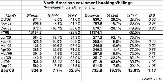
October 21, 2009 – Semiconductor tool orders in September showed year-on-year growth for the first time in nearly two-and-a-half years, more evidence that the industry is climbing out of the deep hole in which it’s been mired, according to the latest monthly data from SEMI.

Worldwide bookings in North America surged to nearly $733M in September, up more than 19% from August; billings rose to nearly $625M, a nearly 8% increase. And we’re finally emerging above water from the beginning of the downturn — bookings were nearly 13% higher than they were in September 2008, the first Y/Y increase since May 2007, and the biggest comparison since January 2007. (The ~8% billings growth would have been even sweeter, except SEMI’s finalization of August numbers upwardly revised the billings by nearly $15M; that improved August’s sequential growth to 7.5% instead of ~5%, and raised the B:B to 1.06 from 1.03.)

Put them together, and the Sept. book-to-bill ratio was a sparkling 1.17, the highest it’s been since Jan. 2008 and the first three-month string of parity since summertime of 2006. That’s $117 worth of orders for every $100 worth of product billed for the month, a ratio that continues to indicate more business coming in than going out.

Click to Enlarge

More evidence that the industry is recovering, slowly: unofficial tally of 3Q09 data (adding the three individual months of July-August-September) gives $1919.1M, which is more than double the bookings in 2Q09 and 73% higher than 1Q09. Sales (which by definition trail orders) also showed growth, up 43% vs. 2Q and nearly 13% higher than 1Q. And tool sales in Japan continue to rev up too, according to the monthly tally from the Semiconductor Equipment Association of Japan (SEAJ). Tool orders in September ramped about 11% to ¥61.567B, while sales spiked about 25% to ¥48.219B, keeping the B:B above parity (1.28) for a fourth consecutive month, the SEAJ notes.

While digesting the tasty news of improving demand and toasting the return of Y/Y growth, let’s not forget to chase it all with a bit of cold water. Growth is good, but we need a lot more of it to achieve levels of sustainability for the industry as a whole — or even find a new level to reset at — especially for a growing number of suppliers and chipmakers who are still clinging on by fingernails (Electroglas being the most recent casualty).

by S.E. Syssoev, A.J. Bartlett, M.J. Eacobacci, Brooks Automation Inc.

EXECUTIVE OVERVIEW
This report summarizes the development of a new cryopump with increased capacity and no short pressure bursts occurring during the cryopumping of type II gases. The new design prevents both possible wafer contamination by uncontrolled intermittent pressure variations inside the high vacuum process chamber, and also the unscheduled shutdown of the processing tool when pressure bursts exceeds certain limits. A 50% higher capacity for type II gas is also achieved with no changes to cryopump external geometry.

One measure of the capacity of a cryopump is established as the quantity of type II gas that can be pumped before the recovery pressure exceeds a specified limit. For a typical physical vapor deposition (PVD) tool, a pressure of 5×10⁻⁶Torr must be achieved within a 5-second interval after the gas flow into the process chamber is stopped (the process is complete).

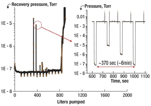
Figure 1 shows the profile of recovery pressure versus quantity of mixed gas (Ar, N2) pumped by Brooks Automation’s On-Board IS 8F cryopump. During typical process operation (gas flow on), the pressure exceeds the abovementioned level by several decades. At ~800L, the recovery pressure rises, indicating the pump is full and regeneration is required. It is desired by semiconductor manufacturers to have a high-capacity cryopump, ensuring less frequent regenerations, which translates into higher tool availability, improved productivity, and lower cost-of-ownership.
Click to Enlarge
Figure 1. Recovery pressure vs. quantity of gas mixture (Ar-N2) pumped shows the pressure burst problem inside the process chamber. Insert shows that the pump is not capable of reaching base pressure after stopping gas flow, which may be falsely interpreted as a full cryopump indication.

Yet another challenging task for a cryopump’s designer is also illustrated by Fig. 1. There have been observed well-pronounced pressure bursts that occasionally last for multi-seconds (see inset). The bursts shown are intermittent in nature and can be mostly seen in situations when a cryopump is pumping a sequence of different process gases or their mixture.

Results in Fig. 1 were obtained for a typical PVD process, which can be characterized by ~30 sec long Ar-N2 flow intervals, each at ~1×10⁻³Torr. These pressure bursts resulted in short-term recovery problems and can be interpreted as a "false full" indication, leading to unnecessary regeneration of the cryopump. An additional effect of such bursts can lead to contamination of the semiconductor substrate if the recovery pressure is not achieved before the substrate is moved into/out of the process chamber.

In this report, we explain the development of a cryopump that eliminates pressure bursts and has significantly increased capacity for type II gases in comparison with the same size pump of the previous design [1].

Higher capacity

The cryopumping of type II gases is essentially similar to thick film growth. The gas flow trapped by the pump can be converted into a deposition rate of the gas molecules onto cold surfaces inside the pump. The majority of these molecules form a thick columnar amorphous film, distributed on the cryo arrays. In turn, the thickness of the deposited layer plays a crucial role in the definition of the cryopump capacity, since condensation and retention of these gases are controlled by the available volume for the frost to grow and the maximum surface temperature of that frost. The typical capacity of the pump we’re discussing is ~1000atm-liters (Ar), which can be interpreted as a piece of frost with the following volume: 

Click to Enlarge

where V and ρ are volume and density of argon at room and cryogenic temperatures.

Used for condensation of gas molecules, the primary pumping area is directly related to the size of the pump. In the case of the 8-inch (200mm) Brooks Automation cryopump, this area is ~250cm2, which makes the thickness of the frost layer equal to about 4cm. To increase capacity of this size pump, the second stage array should be modified in such a way that the distance from its surface to the entrance aperture of the pump is increased in all directions to ensure not only thicker ice (more gas molecules absorbed) but also that a more uniform distribution of the ice is achieved during normal pump operation. Test results confirming design changes that significantly improve capacity are presented in the following section.

Pressure burst-free operation

The volume of the solidified gas estimated in (1) is interesting to compare with the amount of gas participating in the detected pressure burst. From the first principals, the pressure change is proportional to the mass flow: 

Click to Enlarge

where, P — pressure, V — volume, n — number of molecules, R — gas constant, T — temperature, Q — mass flow, S — pumping speed. The total amount of molecules injected during a pressure burst can be found from (2):

Click to Enlarge

The latter allows estimating the volume and (assuming the ice piece is a cube) the side dimension of the cube, which would cause the detected pressure burst in a 50L test system: 

Click to Enlarge

This shows that a piece of frozen gas, which is almost six orders of magnitude smaller than the total volume of the trapped gas, could produce the observed pressure spike. To answer the question on why it would happen, one must refer to the cryo-trapping mechanism. As described earlier, the majority of the gas molecules trapped form a thick columnar amorphous film, distributed on the cryo arrays. Because of the pump geometry, however, there are some zones within the pump that are less exposed to the flow, which limits the rate of deposition of gas species inside these zones to a significantly lower level. This low deposition rate and the mobility of the atoms during film growth play a decisive role in the structural formation of the condensate film [2].

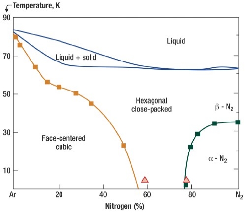
Even for the simple argon/nitrogen binary mixture widely used in most reactive sputtering applications in the semiconductor industry, one can expect formation of polycrystalline (or quasi-crystalline) films with a quite complicated crystallographic structure. In two extremes of the Ar-N2 mixture, shown in Figure 2 (after [3]), either structure with comparable large inter-atomic distance (fcc), or the densest, with the shortest interatomic distance structure (hcp), can be formed within a cryopump’s operation temperature range.
Click to Enlarge
Figure 2. Example of the gas phase diagram, shown for Ar-N2 mixture [2].

In turn, quasi-crystalline films formed inside the abovementioned zones of the cryopump, can be a subject to appreciable residual stress due to the presence of structural defects such as misfit, lattice mismatch, porosity, etc. Clearly, the concentration of these defects is affected by operating conditions such as gas species or gas mixture pumped, rate of deposition, and temperature. All of these factors will also lead to significant variations of the film thickness, at some point reaching a so-called critical thickness [4], after which the film exhibits one of the possible cracking patterns — surface crack, channeling, debond.

In conjunction with the solid gas film grown inside the cryopump, residually stressed film can undergo spontaneous delamination [5], resulting in frost flakes being ejected from the cold surface with subsequent sublimation of the flake on warmer surfaces. The duration and magnitude of the pressure burst that could affect recovery would depend on the size and number of the frost flakes ejected, which is uncontrolled and intermittent in nature. This conclusion is not only applicable for gas mixtures used in the processing of semiconductor materials, but for pure gas cryopumped as well. Once the critical thickness of the film deposited on non-primary surfaces inside the cryopump is reached, similar cracking, debonding, and sublimation sequences are expected, resulting in uncontrolled pressure variations in the process chamber.

Engineering solutions, proposed in this work, were aimed at modifying the existing cryopump in such a way that the amount of frozen gas that can accumulate in the low rate deposition areas are suppressed or significantly limited. In other words, even with some deposition occurring, the thicknesses of the stressed films inside the modified cryopump are kept below the critical value necessary to cause delamination and subsequent sublimation.

Test results

The performance of a modified Brooks Automation On Board IS 8F cryopump was evaluated by using an experimental setup consisting of a vacuum chamber, flow meters, and pressure gauges. The flow rates of argon and/or nitrogen were controlled by mass flow meters calibrated at NIST. The pressure inside the chamber was monitored with a fast-response Granville-Phillips ion gauge, calibrated on a separate setup using the methodology described in [6].

A LabView-based test execution routine was used to precisely simulate typical PVD sputtering processes with respect to the amount and duration of the gas or gas mixture to be used during semiconductor substrate processing. To observe the frost formation inside the pump, a vision system [7] was mounted outside the test chamber and was capable of continuously capturing frost formation on different parts of the cryopump.
 Click to Enlarge
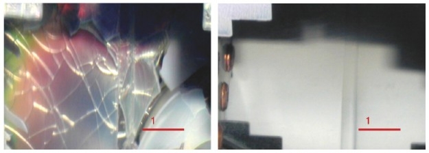
Figure 3. Thin film condensed onto the same non-primary pumping surface: mixed Ar-N2 at ~50L (left, standard design) and ~650L (right, higher performance design) pumped.

Modification of the 8-inch cryopump was made in such a way that all non-primary pumping surfaces, where gas molecules could potentially be deposited due to the temperature of these surfaces, become almost completely hidden from the gas [8]. As a result, during the time needed to reach the pump’s full capacity, the quasi-crystalline film grown in these zones never reached their critical thickness, and did not debond and subsequently sublime.

Figure 3 shows a comparison of the same zones inside the old and newly designed cryopump. As can be seen, even after ~650 liters were pumped, the cryopump of the new design is almost free from formation of the solid deposits on the non-primary surfaces.
Click to Enlarge
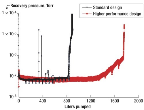
Figure 4. Recovery pressure vs. quantity of mixed gas (Ar-N2) pumped for the cryopumps of standard and higher performance designs.

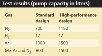
The pressure recovery data presented in Figure 4 demonstrates pressure burst-free operation of the modified cryopump. As predicted, the design changes have also resulted in a significant increase in cryopump capacity for type II gases. The test results shown on the last figure have been achieved using an argon/nitrogen mixture. A summary of all the test data is presented in the table below.
Click to Enlarge


Conclusions

The process of the frost formation inside a cryopump is similar to any thin or thick metal or dielectric film growth — by varying the rate and temperature of growth, one can achieve either a crystal-like structure, or totally amorphous layers. The mechanism of the pressure bursts inside the cryopump discovered in this work is based on delamination of the ice flakes formed on the non-primary pumping surface with subsequent sublimation on warmer surrounding surfaces, which leads to intermittent pressure excursions.

To avoid undesired pressure variations (bursts), formation of highly stressed crystal-like films anywhere on the interior surface of the cryopump needs to be suppressed or limited. Pump capacity strongly depends on the way frost is growing. More uniform distribution of the frost inside the pump leads to increased capacity. In critical semiconductor process applications, the higher capacity maximizes the productivity of the tool by enabling regeneration intervals to be extended to meet the increased operating life of newer targets and/or shields. The modifications applied to this newly developed cryopump are fully transparent to customer processes, providing an exact match for pumping speed, pressure, and time to regenerate with respect to existing product, while achieving the desired performance improvement.

Acknowledgment

The authors would like to thank J.Casello and M.Stira, working for the systems development laboratory, for help in the data collection.

References

1. On-Board IS Cryopump manual, http://www.brooks.com, (2005).
2. M. Layer et al., "Mixing behavior and structural formation of quench-condensed binary mixtures of solid noble gases," Phys. Rev.B 73, 184116 (2006).
3. C. Barrett et al., "Argon-Nitrogen Phase Diagram," J. Chem. Phys., 42, 1, 107 (1965).
4. J. Hutchinson et al., "Mixed mode cracking in layered material," Advances in Applied Mechanics, 29, 63 (1992).
5. H. Yu et al., "Delamination of thin film strips," Thin solid films, 423, 54-63 (2003).
6. K.M.Welch et al., "Recommended Practices for Measuring the Performance and Characteristics of Closed-loop Gaseous Helium Cryopumps," JVST A, 17(5), (1999).
7. Keyence Corporation of America, Unit selection catalog, (2006).
8. A.J.Bartlett et al., "Pressure burst free high capacity cryopump," U.S. Patent Appl. 20080168778, (2008).

Biography

Sergei E. Syssoev received his MS in engineering from St.-Petersburg State Technical U., and a PhD in physics from A.F. Ioffe Institute of Physics and Technology, Russia, and is chief scientist at Brooks Automation, 15 Elizabeth Dr., Chelmsford, MA 01824 USA; [email protected].

Allen J. Bartlett received his formal education at Wentworth Institute and Northeastern U., and is a senior staff engineer at Brooks Automation.

Michael J. Eacobacci received his BSME and a MS in materials science from Northeastern U., and is director of applications engineering at Brooks Automation.

October 13, 2009 – EDA vendor Mentor Graphics has acquired Israeli firm Valor Computerized Systems in a cash-and-stock deal valued at about $82M, or ~$4.60/share of Valor. The deal is expected to close in calendar 1Q10, subject to regulatory and shareholder approval, though the companies noted that 50% of Valor shareholders have committed to vote in favor of the transaction.

Valor makes software to "simulate, optimize, monitor and control the PCB production lifecycle," from testing and validating printed circuit board (PCB) designs to fabrication and assembly. Its Enterprise 3000 software, listed among Mentor’s partner catalog, offers value to Mentor users by "coupling high-level ODB++ data with easy-to-implement automation" for fabrication and assembly analysis and yield optimization.

Valor sales were up about 3% sequentially in the June quarter, with profits up 40% to $1.1M (operating profits slightly down). The company also has a joint venture with Orbotech, Frontline PCB Solutions, to make and sell pre-production CAM and engineering software (much of Valor’s management has an Orbotech pedigree).