Category Archives: Metrology

By Debra Vogler, senior technical editor

March 11, 2011 — Among the topics covered at KLA-Tencor’s annual Lithography Users Forum (2/27/11) at the SPIE Advanced Lithography Conference (2/27-3/3/11) was extension of KLAC’s Teron 600 platform for inspection of EUV blanks at the 16nm half pitch (hp) node.

Click to Enlarge

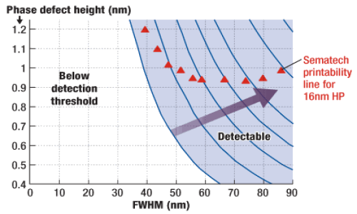
Figure. Blank inspection: Teron platform extension defect signal sufficient for 16nm HP (1 × 50nm FWHM).

When KLAC released the Teron 600 inspection system, the impetus was industry’s need to simultaneously evaluate several lithography technologies for use at the 2Xnm, including spacer pitch splitting/pattern cutting, true pitch splitting, inverse lithography/source mask optimization, as well as EUV. The figure shows simulation results from the 600 platform for inspection of EUV blanks at the 16nm hp node.

Listen to Trafas’ interview:  Download (iPod/iPhone users) or Play Now

In a podcast interview recorded at the event, Brian Trafas, chief marketing officer at KLA-Tencor, discusses the process control needs facing the semiconductor industry, including cost of ownership (COO) and key metrology parameters for 193nm lithography, such as overlay control. One EUV-specific challenge is achieving defect-free masks. To that end, the company has been working on infrastructure needed for mask monitoring (reticle inspection for blanks and patterned masks), as well as patterned wafer defect solutions.      

Subscribe to Solid State Technology/Advanced Packaging.

Follow Solid State Technology on Twitter.com via editors Pete Singer, twitter.com/PetesTweetsPW and Debra Vogler, twitter.com/dvogler_PV_semi.

Or join our Facebook group

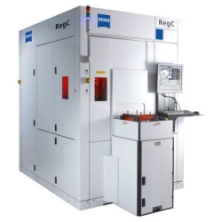
March 3, 2011 — Carl Zeiss introduced a new production tool aimed to improve registration and overlay of advanced photomasks. RegC is based on ZEISS femtosecond-laser technology. RegC enables correction on high-end photomasks for remaining registration errors after the pattern generation process. Current results show registration improvements over 50% in advanced lithography.

Click to Enlarge"This application is targeted to customers who want to beat the lithography roadmaps for overlay and registration, in conjunction with double patterning or other advanced lithography schemes," states Guy Ben-Zvi, managing director of Carl Zeiss SMS Ltd. in Karmiel, Israel. "The RegC system builds a closed-loop application with the ZEISS PROVE registration metrology tool. We developed this system after an extensive survey of our high-end customer base, which had clearly pointed out the emerging need of the industry."

RegC can be used to significantly correct the registration errors of any single photomask or groups of photomasks of the same mask set towards optimal wafer overlay values. Even the small pellicle impact on the overall registration budget can be corrected, as the RegC process can be run after the pellicle has been applied.

Fast turnaround time and seamless integration in any advanced mask manufacturing cycle allow users to save pattern generation tool time. The need of rewriting masks due to registration errors can be avoided and the mask process flow in the mask shop does not need to be interrupted.

Carl Zeiss presents the new tool RegC on SPIE Advanced Lithograpy in San Jose, CA, February 27 through March 4, 2011. 
More SPIE news:

Subscribe to Solid State Technology/Advanced Packaging.

Follow Solid State Technology on Twitter.com via editors Pete Singer, twitter.com/PetesTweetsPW and Debra Vogler, twitter.com/dvogler_PV_semi.

Or join our Facebook group

March 2, 2011 – PR Newswire — At SPIE Advanced Lithography 2011, Cymer Inc. (Nasdaq: CYMI), light sources supplier to chipmakers to pattern advanced semiconductor chips, introduced a focus drilling technology for its immersion light sources including the XLR 600ix, XLR500i, XLA 400 and XLA 300. Focus drilling provides up to a 2X improvement in the depth of focus on the wafer, thereby enabling a larger process window that can positively impact chipmakers’ yield.

Laser focus drilling technology was developed to aid chipmakers in patterning deep contact and via structures with thick resists where high depth of focus is required. Cymer’s focus drilling product is supported by a technique involving operation of the light source at multiple bandwidths, utilizing metrology that was designed to measure high-bandwidth spectra. Additionally, the unique spectral shape of Cymer’s light sources can improve depth of focus with minimal impact on other key process parameters.

More than five years of development effort at Cymer went into investigating multiple approaches to improving depth of focus through spectral engineering, said Ed Brown, president and chief operating officer of Cymer. "Our close collaboration over the past year with our direct scanner and chipmaker customers was instrumental."

Light sources equipped with focus drilling are being qualified, and are currently under chipmaker evaluation.

Click here to listen to an interview with Cymer’s Nigel Farrar about EUV, DUV, focus drilling, and lithography advances.

SPIE Advanced Lithography’s exhibition wraps up today in San Jose, CA, with conferences finishing on March 3.

Cymer, Inc. (Nasdaq: CYMI) develops light sources used by chipmakers worldwide to pattern advanced semiconductor chips, and is pioneering a new silicon crystallization system for the flat panel display industry. Please visit www.cymer.com.

Subscribe to Solid State Technology/Advanced Packaging.

Follow Solid State Technology on Twitter.com via editors Pete Singer, twitter.com/PetesTweetsPW and Debra Vogler, twitter.com/dvogler_PV_semi.

Or join our Facebook group

March 1, 2011 – Business Wire — Nanometrics Incorporated (Nasdaq:NANO), advanced process control metrology provider, launched the Mosaic II turnkey image-based overlay metrology solution for advanced high-volume IC manufacturing. NANO reports an initial delivery to a leading Asian memory customer.

With the launch of the Mosaic II, Nanometrics supports advanced lithography process control, including double patterning processes used on today’s most advanced devices, commented David Doyle, vice president and business unit manager of Nanometrics. "We continue to strengthen our product offerings in this important market with a major Asian customer selecting the Mosaic II system for production line monitoring of their most challenging devices."

The Mosaic II is designed as part of Nanometrics’ Lynx cluster metrology platform, combining Mosaic II with IMPULSE modules onto a Lynx metrology cluster. This configuration would enable image-based overlay, diffraction-based overlay (DBO) and optical critical dimension (OCD) measurements. Earlier generation Caliper Mosaic tools can be field upgraded to Mosaic II capability.

To learn more about the Mosaic II, Lynx cluster metrology, and Nanometrics process control metrology solutions, visit Nanometrics at SPIE Advanced Lithography, San Jose Convention Center, through March 2 at Booth 324.
More SPIE news:

Nanometrics provides advanced, high-performance process control metrology systems used primarily in the fabrication of semiconductors, high-brightness LEDs, data storage devices and solar photovoltaics. Nanometrics’ website is http://www.nanometrics.com.


Copyright 2011 Business Wire

Subscribe to Solid State Technology/Advanced Packaging.

Follow Solid State Technology on Twitter.com via editors Pete Singer, twitter.com/PetesTweetsPW and Debra Vogler, twitter.com/dvogler_PV_semi.

Or join our Facebook group

Executive Overview

The semiconductor industry is still in the early deployment phase of using high-k metal gates (HKMG) to overcome high leakage currents and higher power consumption of advanced devices. A particular challenge associated with implementing HKMGs is monitoring gate height. This article describes how picosecond ultrasonic technology can be used during various stages of process development, integration, and volume manufacturing for monitoring the HKMG stack.

J. Dai, P. Mukundhan, J. Chen, J. Tan, Rudolph Technologies, Flanders, NJ USA
D.B. Hsieh, T.C. Tsai, 1-United Microelectronics Corp., Tainan, Taiwan

High-k metal gates are a relatively new development in semiconductor manufacturing. Traditional gate architectures use polysilicon gate electrodes and silicon dioxide gate dielectrics, but these materials present difficulties at 45nm and below. Most notably, thinner gate oxides lead to high leakage currents, gate oxide breakdown, and dopant migration [1-2], creating untenable power consumption and reducing device reliability. High-k materials overcome these problems by enabling thicker gate dielectrics that reduce leakage current while maintaining high gate capacitance. Because the high-k materials are not compatible with polysilicon gate electrodes, a metal (typically aluminum) is used instead, hence the name high-k metal gate (HKMG).

Although at least one leading manufacturer is already in full production with advanced generation HKMG processes, the industry as a whole is still in the early deployment phase. The HKMG combination is important for all emerging applications that require high-performance and low gate-leakage, including all silicon and non-silicon nanoelectronic transistors (III-V materials, carbon nanotubes) [3]. It is being adopted by most IDMs and foundries due to its lower thermal budget, more stable threshold voltage, and better performance from strain-induced dummy gate removal than the alternative gate-first approach.

HKMG CMP process metrology

The gate height is critical to transistor performance and precisely controlling the gate height and uniformity is the primary challenge for the replacement metal gate aluminum CMP process. Non-uniform gate height can cause gate resistance variation, and improper gate heights can result in subsequent contact etch problems. Aluminum CMP is used to remove the Al overburden and work function metals from the field after Al gap fill. The gate height is only several hundred Angstroms, so the Al CMP process tolerance is much tighter than conventional CMP processes. This requires extremely tight within-wafer (WIW) and wafer-to-wafer (WTW) control of the Al polish for it is to meet gate height uniformity requirements.

Cross-sectional TEM (transmission electron microscopy) is often used to characterize gate height and thickness of work function metals during the research and development phase. X-ray reflectometry (XRR) has been used for thickness measurement on blanket wafers without the requirement for reference samples. However its accuracy strongly depends on modeling to adapt to graded layer, interface, roughness, and density, especially for thin films (a few hundred Angstroms). XRR also has an upper limit on thickness (< 3000Å) and cannot be used for pre-CMP Al measurements, where typical thickness values are ~8000 or 9000Å. Also, because of the beam’s grazing incidence, the effective spot size on the wafer can be as large as a few millimeters, making it unusable for direct measurement of gate thickness on product wafers.

X-ray fluorescence (XRF) can measure thickness, but it cannot be readily extended to in-line monitoring of HKMG stacks for some of the reasons discussed below. Even μ-XRF techniques, with spot sizes of 30μm (based on full width at half maximum, i.e., FWHM), are still not small enough to measure on 40μm x 40μm or smaller measurement sites because the effective beam spot, the area that X-ray beam actually covers on films, is about two times bigger. Additionally, measurements with enough precision for gauge capability require data acquisition times that are too long for use in in-line production monitoring. XRF also has limited sensitivity for aluminum and other lighter elements with the atomic number less than that of Si because of the limitations of the Be window of the Si(Li) detector. This, coupled with the uncertainty of placing the X-ray beam at same position on each measurement site adds more to the challenges of measuring such small and non-uniform patterned structures. A laser-interferometer based in situ rate monitor (ISRM), for Al CMP endpoint detection, is often integrated in the CMP system, but it usually does not have enough accuracy and resolution for process monitoring.

Resistivity-based measurements of film thickness also face challenges on very thin films in the HKMG stack, such as the work function metals, which may be 100Å or less. The thickness of the film itself begins to influence the bulk electrical conductivity of the material, and boundary scattering occurs as electrons that would normally bounce off atoms in the film go through to the cladding layers. At this point, the simple relationship between film thickness to series resistance and bulk resistivity breaks down.

For aluminum, 300Å is the lower limit, and for Ti, 200Å. In contrast to TEM, XRR, XRF, and resistivity measurement, the picosecond ultrasonic [4] technique offers an ideal inline on product measurement metrology for monitoring both aluminum and work function (WF) metals. A 0.1ps laser pulse (pump) is focused to about 5×7μm2 spot onto a wafer surface to create a sharp acoustic wave. The acoustic wave then travels away from the surface through the film at the speed of sound. At an interface between materials, a portion of the acoustic wave is reflected back toward the surface while the rest is transmitted. When the reflected acoustic wave reaches the wafer surface, it is detected by another focused laser pulse (probe) which was diverted from the pump pulse by a beam splitter and delayed by a servo controlled variable delay optical circuit. The non-contact, non-destructive nature of this technology enables thickness measurements from tens of Angstroms to 8 microns directly on product wafers. The small spot size (5μm × 7μm2) allows for measurements at site sizes of 30μm x 30μm. Measurements are based on first principles and do not require daily calibrations or reference wafers. In addition to thickness measurements, other parameters such as roughness, density, phase and modulus can be determined to provide additional information about the process.

Pulse measurements in the HKMG process flow

Picosecond ultrasonic measurements are used as checkpoints during various stages of development, integration, and manufacturing of high-k/metal gates. Results from pre- and post-CMP characterization, as well as process tool qualification for work function materials, are discussed.

Pre-CMP characterization and process optimization. Four blanket wafers, two pre-CMP (4000Å and 8000Å) and two post-CMP (polished to baselines [BSLs] BSL+60s from 8000Å as deposited, respectively) wafers were prepared, and picosecond measurements were used to characterize the as-deposited and post-CMP aluminum metal gate in order to fine-tune the Al growth process. Because of the small measurement spot size, measurements can be made to within 1mm edge exclusion to provide information on the edge profiles.

Figure 1. Line scan across the wafer showing the aluminum thickness profile from -149 to 149mm (top left) and roughness profile (top right),high resolution thickness (lower left) and roughness(lower right) edge profiles from -149 to -141mm.

Rapid measurements (2-3s per site) make it possible to acquire 49-point within-wafer uniformity maps as well as high resolution line and edge scans to characterize plating profiles. Across-wafer line scans (Fig. 1) from -149mm to 149mm were made to characterize the Al thickness and roughness variation across the wafer. Because of the small measurement spot size, very high resolution edge scans were also made on all the wafers. Figure 2 shows very symmetric profiles of aluminum thickness~target +1.2kÅ at 1mm exclusion decreasing to target-2kÅ closer to 5mm exclusion, and the very constant roughness (target+/-25Å) even at the wafer edges.

Figure 2. Cross-section TEM graphs of the four aluminum films: a) Pre-CMP 8K, b) CMP BSL, c) Pre-CMP 4K and d) CMP BSL+60s. Correlation between picosecond ultrasonic measurements and TEM on pre- CMP and post-CMP wafers is excellent (R2=0.99).

During process optimization, roughness measurements are also used as a qualitative gauge to indicate the presence of pinhole defects. Roughness measurements showed excellent correlation (R2=0.99) to RMS roughness measured using AFM. Accuracy of the PULSE measurements was verified by performing cross-sectional TEM analysis (Fig. 2).

Figure 2 shows the very good correlation between the measurements and cross-sectional TEM thickness. The excellent correlation validates picosecond ultrasonic capability for pre-CMP and post-CMP Al film measurements. Repeatability measurements, both static and dynamic (load/unload) have been tested. The 1σ standard deviation for static and dynamic repeatability is ~ 0.1% and 0.2%, respectively. Long term stability performance on the pre-CMP wafer showed a 1σ standard deviation of ~ 0.01%, confirming that the technique is sufficiently stable and reliable for production monitoring. With information provided from picosecond ultrasonics, process parameters can be optimized and measurements can be made directly on product wafers, eliminating the need for monitor wafers.

Characterization of work function metals. PULSE measurements on the work function and barrier metals were tested. 1σ standard deviation for both static and dynamic repeats is ~ 0.3% or less. Figure 3 shows a cross-section TEM micrograph of a 60Å TiN stack and a 49-point line scan profiles across different barrier wafers. All the films showed profiles consistent with the process. The technology has been successfully and routinely used for similar metal film applications in both the FEOL and BEOL applications. The current performance on the work function metals is consistent with the capability of the technique.

Figure 3. Cross-section TEM micrograph of TiN barrier metal and 49-point line scans across the wafer for various barrier metal layers used in the HKMG structure

Post-CMP characterization on array structures. The critical requirement for production monitoring of the HKMG process is the ability to measure in small test structures, ~ 30μmx30μm, to determine the gate height and uniformity. Post-CMP measurements of the gate stack were made on various sub-micron array structures in ~30μmx30μm sites. Various array structures were investigated for both N-well and P-well stacks of varying array widths with a density of 75%. In this study, results from measurements on 30μmx30μm test features with 5 micron pad arrays were used to demonstrate the capability of picosecond ultrasonic technology.

Figure 4. A best-fit model to picosecond ultrasonic measurement on 5µm pad array after CMP. The thickness for Al gate height as well as the total thickness of barrier and work function materials can be determined from this signal.

Figure 4 shows a picosecond ultrasonic measurement and the best fit model on a 5μm pad array after CMP. Using picosecond ultrasonic technology, thickness for aluminum gate height and combined barrier and work function thickness can be measured simultaneously. Cross-sectional measurements verified the accuracy of these results for a wide thickness range.

Conclusion

Picosecond ultrasonic technology can be used during various stages of process development, integration, and volume manufacturing for monitoring the HKMG stack. Information can be used to characterize the process, and optimize deposition and CMP processes. The accuracy of the technique for monitoring advanced HKMG gate stacks has been confirmed by TEM measurements. The small spot, non-destructive nature of this technology allows for measurements in 30μmx30μm sites directly on product wafers at production-worthy throughputs. The technology offers a complete and ideal metrology tool for non-destructive, non-contact, direct measurement on both blanket and product wafers. Its capability has been extensively proven for both pre-CMP and post-CMP for aluminum processes. The ability to characterize work function barrier layers provides an additional benefit for the use of the technology for HKMG process monitoring.

Acknowledgments

S.F. Huang, Y. R. Yang, C. L. Yang , and J. Y. Wu of 1-United Microelectronics Corp. are co-authors. PULSE is a trademark of Rudolph Technologies.

References

  1. M. Bohr, R. Chau, T. Ghani, K. Mistry, IEEE Spectrum, Oct. (2007) pp. 30-35.
  2. V. Misra, G. Lucovsky, G. Parsons, MRS Bulletin, vol 27, no3, (2001) pp. 212-216.
  3. R.Chau, J. Brask, S. Datta, G. Dewey, M. Doczy, B. Doyle, et al., Microelectronic Engineering, vol 80, June (2005) pp. 1-6.
  4. C. Thomsen, H. T. Grahn, H. J. Maris, J. Tauc, Phys. Rev B, vol 34, no 6, (1986) pp. 4129-4138.
  5. M. Hsieh, J. Yeh, M. Tasi, K. Wang, J. Tan, S. Leary, Proc. SPIE, Vol. 6152, 61522C, March (2006) pp. 815-828.

Biographies

Johnny Dai received his PhD at Fudan U., Shanghai and is a principal applications scientist at Rudolph Technologies, One Rudolph Road, P.O. Box 1000, Flanders, NJ 07836 USA; ph: 973-448-4479; email [email protected].

Solid State Technology | Volume 54 | Issue 3 | March 2011

More Solid State Technology Current Issue Articles
More Solid State Technology Archives Issue Articles
February 25, 2011 — SoftJin Technologies, a provider of customized automation software for electronic design and manufacturing, enhanced NxDAT, its defect analysis software. NxDAT is used by mask shops and wafer foundries for efficient analysis of defects identified by IC photomask inspection systems. NxDAT, with its open architecture, can be easily extended for analysis of defects identified by a variety of inspection equipments including integrated circuit (IC)/flat panel display (FPD) mask inspection, wafer inspection, and metrology systems.

NxDAT includes features for navigation, visualization, sophisticated image measurement, cross-section analysis and repeatability analysis for accurate analysis and classification of defects. The enhanced version of NxDAT is optimized for better speed and memory performance. New analysis options in the Defect Image Analysis and Defect-to-CAD Database correlation area provide more insight into defects’ nature. New usability improvement features include customizable GUI layout, batch mode support, property-based file opening and user-defined filters.

As part of Open Architecture support in NxDAT, SoftJin provides a generic Reader/Writer Plug-In interface through which various defect file formats can be easily supported. The new version of NxDAT supports SEMI’s P41-0304E Mask defect data specification standard. With its capability of loading and stacking multiple inspections in different formats, NxDAT can be used as common defect analysis software for various inspection equipments.

NxDAT supports correlation of mask defect data with CAD Layout data in major industry standard IC layout and mask data formats. SoftJin has now enhanced this feature by providing direct interface with HOTSCOPE Layout and Mask data Viewer. HOTSCOPE, an industry standard layout and mask data viewer from Jedat Inc. (Japan), is capable of reading and displaying huge-sized mask data quickly and accurately. With HOTSCOPE interface in NxDAT, user can navigate through the defect data in NxDAT and at the same time visualize the corresponding region of CAD data in HOTSCOPE, enabling design based defect criticality analysis.

Key new features in the enhanced version of NxDAT include:

  • Image enhancement options such as display of defect region as zoomed images, multi-level threshold images and overlay of gray level matrix on the image
  • Automatic registration of images enabling the user to analyze the correctly aligned images
  • Scripting interface to run the software in Batch mode. Batch mode enables user to automate tasks in the defect analysis flow.
  • Multi-tier classification support to add any number of secondary classifications. As an example, primary classification could be for defect type, and a secondary classification could be used for disposition or action to be applied on the defect after analysis.
  • CAD data correlation support for OASIS.MASK along with the existing GDSII, OASIS, MEBES, OASIS.VSB formats
  • User defined GUI layout option to customize and save the preferred layout configuration of NxDAT 
  • Property based file opening feature to select defect files based on the reticle name, inspection name, barcodes etc.
  • Regression plots between various attributes of defect data
  • Automatic Binning of defects using programmable ranking function based on defect criteria such as defect area, CD etc.

With the performance improvements in latest version of NxDAT, opening a 10,000 defect file takes less than a minute on inexpensive PCs and navigating between defects is instantaneous.

SoftJin also offers NxDAT customization services wherein NxDAT can be enhanced as per the specific needs of the equipment vendor or end user.

SoftJin Technologies develops Innovative and Customized Automation software for Electronic Design and Manufacturing. For more details and feature list of NxDAT, please visit http://www.softjin.com/nxdat   

Subscribe to Solid State Technology/Advanced Packaging.

Follow Solid State Technology on Twitter.com via editors Pete Singer, twitter.com/PetesTweetsPW and Debra Vogler, twitter.com/dvogler_PV_semi.

Or join our Facebook group

February 24, 2011 – Business Wire — Nanometrics Incorporated (NASDAQ:NANO), advanced process control metrology system supplier, installed a next-gen UniFire 7900IR metrology system at a leading manufacturer of advanced logic devices. The Unifire 7900IR provides 3D inspection of wafer-scale packaging features as well as registration for wafer-to-wafer bonding applications for use in advanced wafer scale packaging process control.

"Careful control of lithography and etching in the through silicon via (TSV) flow, bumping, and wafer-to-wafer bonding processes is critical to enable high yielding devices for next generation advanced packaging. This latest system offers a new 3D inspection capability as well as an infrared (IR) microscope option, allowing direct measurement of features and structures in bonded wafer stacks," commented Dr. Michael Darwin, VP of the UniFire and Materials Characterization Groups at Nanometrics.

Existing UniFire systems can be field upgraded with both IR and 3D inspection options to further extend the capability of installed tools.

To learn more about the UniFire 7900IR and Nanometrics process control metrology solutions, visit Nanometrics at SPIE Advanced Lithography, San Jose Convention Center, March 1st-2nd.

Nanometrics provides advanced, high-performance process control metrology systems used primarily in the fabrication of semiconductors, high-brightness LEDs, data storage devices and solar photovoltaics. Nanometrics is traded on NASDAQ Global Select Market under the symbol NANO. Nanometrics’ website is http://www.nanometrics.com

Subscribe to Solid State Technology/Advanced Packaging.

Follow Advanced Packaging on Twitter.com by clicking www.twitter.com/advpackaging. Or join our Facebook group

February 24, 2011 – PR Newswire — Novellus Systems (Nasdaq: NVLS) subsidiary Peter Wolters GmbH introduced a new version of its microLine double side lapping system for prime silicon wafers. The AC-2100L system features independently driven inner and outer pin rings, automatic force calibration, and in-situ wafer thickness metrology for closed-loop process control. The system can process up to 20 300mm wafers in one batch, while exceeding the latest wafer geometry requirements.

Figure 1. The AC 2100-L microLine double side lapping system. (PRNewsFoto/Novellus Systems, Inc.)

Double-side lapping for prime silicon wafer manufacturing offers high throughput, precise wafer geometry control, and lower cost of consumables. Independently driven inner and outer pin rings (Figure 2) enable maximum process control. Automatic force calibration compensates for weight loss of the upper lapping wheel due to typical process wear, ensuring accurate force control over the entire wheel life. Contactless gauges control the lapping wheel gap dimension, thus ensuring repeatable within batch and batch-to-batch wafer thickness throughout the lapping process. Additionally, the system can be configured with a non-contact, optical gauge developed by Peter Wolters for in-situ measurement and control of wafer thickness. This technology provides wafer manufacturers with the submicron precision (Figure 3).

Figure 2. Independent inner and out pin rings for maximum process flexibility. (PRNewsFoto/Novellus Systems, Inc.)

The AC-2100L’s new, larger lapping wheel has an outside diameter of 2100mm. The larger wheel allows the use of five carrier rings, resulting in a 20 wafer batch size. For ease of cleaning, maintenance and wheel replacement, the machine head on the AC-2100L swivels out. The operator interface (HMI) is based on the well-established AC-2000 platform.

Figure 3. Non-contact, optical gauge provides in-situ submicron control of wafer thickness (Sample size: 460 wafers). (PRNewsFoto/Novellus Systems, Inc.)

"While designed for today’s 300mm wafers, the AC-2100L can also simultaneously process up to 8 450mm wafers, thus preparing Peter Wolters’ customers for the next wafer size transition," said Kay Petersen, chief executive officer of Novellus’ Industrial Applications Group.

Peter Wolters GmbH, part of Novellus’ Industrial Applications Group, manufactures high-precision surface polishing systems for substrates made of silicon, sapphire, gallium arsenide, silicon carbide and other materials used to manufacture microelectronic, micro-optical, and micromechanical devices. For more information on Peter Wolters, visit www.peter-wolters.com

Novellus Systems, Inc. (Nasdaq: NVLS) is a leading provider of advanced process equipment for the global semiconductor industry. For more information about the AC-2100L, please visit www.novellustechnews.com

SOURCE Novellus Systems, Inc. Copyright 2011 PR Newswire Association LLC

Subscribe to Solid State Technology/Advanced Packaging.

Follow Solid State Technology on Twitter.com via editors Pete Singer, twitter.com/PetesTweetsPW and Debra Vogler, twitter.com/dvogler_PV_semi.

Or join our Facebook group

February 11, 2011 — Avantor Performance Materials, Inc. (formerly Mallinckrodt Baker, Inc.) plans to open an electronics applications laboratory in Taiwan during the second quarter of 2011. The new laboratory will be used to conduct customer demonstrations, perform process of record (POR) development and support Avantor’s global electronics technologies development.

Avantor is opening the Asia-based electronics laboratory to support global customers more quickly with access to advanced wafer processing and metrology tools. Customers will now be able to use Avantorís state-of-the-art equipment to test chemistries and materials in a class 100 clean room fab environment, rather than disrupting operations by taking their own production equipment off-line for testing purposes.

"As customers implement our performance chemistries into their processes, they can test and make refinements on Avantor’s laboratory tools and transfer those processes back to their fabs, without ever having to interrupt their workflow," said Director of Marketing, Electronic Materials, John Bubel.

Additionally, Bubel noted that Avantor will test newly developed formulas on its full wafer equipment to support its own performance chemistries, and materials research and development.

"We are designating space for research and development, and production of small volume sample materials to better meet the needs of our global customers," he added.

Avantor currently has applications or research and development laboratories in the United States, Korea and the Netherlands.

Avantor Performance Materials, formerly Mallinckrodt Baker, manufactures and markets high-performance chemistries and materials under J.T.Baker and Macron Chemicals (formerly Mallinckrodt Chemicals) designations. These products are used in electronics and photovoltaic (PV) manufacturing; biotechnology and pharmaceutical production; and in research, academic and quality control laboratories. For additional information please visit www.avantormaterials.com.

Subscribe to Solid State Technology/Advanced Packaging.

Follow Solid State Technology on Twitter.com via editors Pete Singer,
http://twitter.com/PetesTweetsPW and Debra Vogler, http://twitter.com/dvogler_PV_semi. Or join our Facebook group.

February 1, 2011 — Leica Microsystems and Digital Surf announced an agreement whereby Leica Map surface imaging and metrology software, based on Digital Surf’s Mountains Technology, will be used with the Leica Application Suite (LAS) for Leica industrial microscopes. The Leica Map software is used to visualize and quantify features of measured surfaces, characterize surface texture and geometry, and generate visual surface metrology reports with full traceability. It is available on three levels with optional modules for advanced applications.

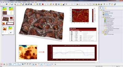
Click to EnlargeEntry-level Leica Map Start software is used in conjunction with LAS Montage. LAS Montage acquires a series of image planes at known spacing covering the in-focus region of a specimen with a Leica microscope. From this stack a depth map and an extended focus image are derived and analyzed by Leica Map. In Leica Map Start, surface topography can be viewed at any zoom level and any angle in real time. Color and intensity image overlays facilitate the location of surface features, including defects. Distances, angles, and step heights can be measured. Height and functional parameters are calculated in accordance with the latest ISO 25178 standard on areal surface texture. Optional modules can extend the capability to surface texture and contour analysis.

Leica Map DCM 3D software is dedicated to the Leica dual core 3D microscope Leica DCM 3D, which combines confocal and interferometry technology for non-invasive, high speed, and high-resolution assessment of micro and nano structures. In addition to the standard features of Leica Map Start, Leica Map DCM 3D includes advanced ISO 16610 filtering techniques for separating surface roughness and waviness, basic functional analysis (bearing ratio, depth distribution, etc.), and the ability to extract sub-surfaces (for example from mechanical and electronic components and MEMS) and analyze them independently.

Leica Map Premium is a top of the line universal solution that is compatible with single-point tactile and optical profilometers and scanning probe microscopes, as well as with optical microscopes.

"Leica Map software is based on the latest generation of Mountains Technology, which was released in the second half of 2010," stated François Blateyron, COO of Digital Surf. "It incorporates an enhanced desktop publishing environment, to speed up complex calculations and the processing of large measurement data sets."

Leica Microsystems provides microscopes and scientific instruments. Leica Microsystems is organized in four divisions: the Life Science Division, Industry Division, Biosystems Division and Medical Division.

Digital Surf provides imaging and analysis software for surface metrology instruments including confocal microscopes, optical interferometric microscopes, scanning probe microscopes and 2D/3D profilometers.

Follow Small Times on Twitter.com by clicking www.twitter.com/smalltimes. Or join our Facebook group