Category Archives: Touch Technologies

March 11, 2011 — Oxford Nanopore Technologies Ltd signed an exclusive agreement with Harvard University’s Office of Technology Development for the development of graphene for DNA sequencing. Under the terms of the agreement, Oxford Nanopore has exclusive rights to develop and commercialize methods for the use of graphene for the analysis of DNA and RNA, developed in the Harvard laboratories of Professors Jene Golovchenko, Daniel Branton, and Charles Lieber.

Graphene is a single-atom thick lattice of carbon with high electrical conductivity. These properties make it an ideal material for high resolution, nanopore-based sequencing of single DNA molecules.

The agreement adds to an existing collaboration between Oxford Nanopore and Harvard that spans basic methods of nanopore sensing through to the use of solid-state nanopores. Oxford Nanopore will also continue to support fundamental nanopore research at Harvard.

Dr Gordon Sanghera, CEO of Oxford Nanopore Technologies, explained that the "groundbreaking research at Harvard lays the foundation for the development of a novel solid-state DNA sequencing device."

"Oxford Nanopore is probably best known for protein nanopores,” continued Dr Sanghera. "However, today’s agreement highlights that we are increasing our investment in solid-state nanopores by adding graphene to our existing portfolio of solid-state nanopore projects and collaborations."

The Harvard team and collaborators used graphene to separate two chambers containing ionic solutions, and created a hole — a nanopore — in the graphene. The group demonstrated that the graphene nanopore could be used as a trans-electrode, measuring a current flowing through the nanopore between two chambers. The trans-electrode was used to measure variations in the current as a single molecule of DNA was passed through the nanopore. This resulted in a characteristic electrical signal that reflected the size and conformation of the DNA molecule. The work was presented in a 2010 Nature publication (S. Garaj et al, Nature Vol 467,doi:10.1038/nature09379).

Graphene is believed to be the thinnest membrane able to separate two liquid compartments from each other. This is an important characteristic for DNA sequencing; a trans-electrode of this thickness would be suitable for the accurate analysis of individual bases on a DNA polymer as it passes through the graphene.

Nanopore techniques aim to improve substantially the cost, power and complexity of DNA sequencing. While first-generation technologies in development at Oxford Nanopore use nanopores made by porous proteins, subsequent generations will use synthetic solid-state materials such as silicon nitride. Challenges remain in industrial fabrication of synthetic nanopores with the required dimensions and electronic properties. Graphene offers a potential solution due to its strength, dimensions, electrical properties and future potential for low-cost manufacturing.

Oxford Nanopore Technologies Ltd is developing a novel technology for direct, electronic detection and analysis of single molecules using nanopores. The company also has collaborations for the development of solid-state nanopores. Learn more at http://www.nanoporetech.com/

Nature publication: Graphene as a subnanometre trans-electrode membrane, S. Garaj, W. Hubbard, A. Reina, J. Kong, D. Branton & J. A. Golovchenko. Nature Vol 467,doi:10.1038/nature09379 (Sept 2010)
This publication describes the use of graphene as a trans-electrode, detecting a DNA strand as it passes through a hole in the graphene sheet. A sheet of graphene was stretched over a silicon-based frame, and inserted between two separate liquid reservoirs. An electrical voltage was applied between the reservoirs and when a nanopore was formed in the graphene this allowed the flow of an ionic current through the nanopore.

This current could be measured as an electrical current signal using the trans-electrode properties of graphene. Double-stranded DNA strands were added to one chamber and electrophoretically driven through the nanopore. This created a characteristic electrical signal that reflected the size and conformation of the DNA molecule. Graphene is thin enough to interact with individual nucleotides on a DNA strand as it passes through the nanopore, and therefore suitable for further development as a solid state DNA sequencing tool. Graphene Graphene is a single atom thick sheet of carbon – one layer of graphite. The carbon atoms are arranged in a hexagonal planar structure. Graphene has extremely high strength-to-weight ratio and has higher electrical conductivity than silicon. The material has been proposed as suitable for many future applications including a range of electronic nanodevices, batteries, touch screens, transmitters and receivers for broadband communications.

Follow Small Times on Twitter.com by clicking www.twitter.com/smalltimes. Or join our Facebook group

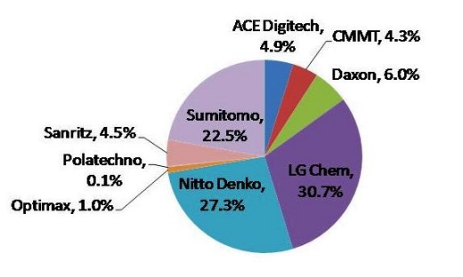
February 1, 2011 — Displaybank, market research and consulting provider for the display industry, reports that LG Chemical secured its number one position in the large-area TFT-LCD polarizer market for the second straight year. LG Chemical has 30.7% market share, followed by Nitto Denko with 27.3% share and Sumitomo Chem. with 22.5% share. For the large-area TFT-LCD polarizer market in 2010, these top 3 suppliers’ market share exceeded 80% of the total market. These and other findings are disclosed in Displaybank newly updated "Polarizer and Optical Films Industry Trend Analysis," which covers global polarizer market in detail on a quarterly basis.

Click to Enlarge
Figure 1. Large-area TFT-LCD polarizer market share by maker (Area-basis, Y2010). Source: Polarizer and Optical Films Industry Trend Analysis, Displaybank January 2011.

As value-added polarizer demand rises including polarizer for LEDs, 3D, and touch panel displays, market share for these top 3 makers shows continuous growth. Irene Heo, senior analyst at Displaybank, noted "the industry dependence towards these top 3 polarizer makers will continue to go up in 2011, as the makers have manufacturing know-how for value-added films and also secure higher price competitiveness against other makers."

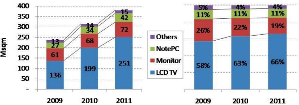
Area basis (Msqm) 2009 2010  2011   Revenue basis (USD million) 2009 2010 2011
 LCD TV 136  199  251     LCD TV 3,488  4,946  5,670
Monitor  61  68  72     Monitor  1,884  2,084  2,092
Notebook PC 27 34 42   Notebook PC  864   1,068 1,221
Others 13 14 15   Others 991 1,090 1,162
Total 236  315  380     Total  7,227  9,188  10,145
Tables. Polarizer markets by major application. Source: Polarizer and Optical Films Industry Trend Analysis, Displaybank January 2011.

As new line operation and decreased demand during 2H 2010 led to a drop in polarizer price, the overall polarizer market in 2010 is estimated at $9.18 billion, slightly lower than previous expectation. In terms of area-basis, the market is estimated to have grown 24% from 2009 to 320 million square meters in 2010.

Click to Enlarge
Figure 2. Polarizer market forecast by application (Area-basis). Source: Polarizer and Optical Films Industry Trend Analysis, Displaybank January 2011.

By major application, TV-use polarizer market reached $4.95 billion (54% of applications) in 2010; monitor-use polarizer use  hit $2.08 billion; notebook-use polarizers reached $1.07 billion. In terms of area-basis, TV-use polarizer reached 200 million square meters: 63% of the total market.

Heo noted "in 2011, large-area polarizer market is expected to exceed $10.1B to grow 10.4% Y/Y and TV-use and notebook-use polarizer will each grow 14.6% and 14.3% Y/Y respectively."

Access "Polarizer and Optical Films Industry Trend Analysis" at http://www.displaybank.com/eng/report/report_show.php?id=15

Displaybank is a global authority in market research and consulting for the electronic display industry. Displaybank’s analysts are located throughout Korea, Japan, China, Taiwan, and the U.S. For more information, visit www.displaybank.com.

Follow Solid State Technology on Twitter.com via editors Pete Singer, twitter.com/PetesTweetsPW and Debra Vogler, twitter.com/dvogler_PV_semi.

Or join our Facebook group

December 10, 2010 – IC shipments are surging again as the key PC market rebounds off three dismal years with renewed strength thanks to portable computers, which are widening the sales gap with chip-stalwart desktop systems (including systems used as servers), notes IC Insights.

PCs are still the largest end-use application for ICs (31% of total 2010 revenues), and will snap a three-year slump in 2010 by growing 18% to 351M units shipped. Sales value of the ICs in those PCs will surge about 34% to a record $81.4B. IC Insights sees 12% PC shipment growth in 2011 (394M units), while PC ICs fall back to 10% growth ($89.2B). PC ICs will enjoy a ~11% CAGR for the entire 2009-2014 period, reaching $101.2B in that final year.

But within that growth in PC ICs, it’s important to understand that the real driver is portable systems, whose low-power and battery management requirements means using higher-priced chips than desktop systems. Portable PCs overtook desktops in 2009 (157M units vs. 140M) and should grow 27% in 2010 to ~200M units, vs. just 8% for desktop ICs to 151M, IC Insights calculates. And that gap is growing — the firm expects 242M portable PC shipments in 2011 vs. 152M for desktops, growth of 21% vs. a meager 1%.

And within that portable PC segment are other important trends. Notebook shipments are seen growing 20% to 155M units; mini-notebooks (aka "netbooks"), "the darling of the portable PC market in 2008 and 2009" nearly tripling in size each of those years, will be up just 19% to 31M units. Give credit to the tablet computing revolution ushered in by Apple’s touchscreen iPad; this sector (excluding dedicated e-book readers e.g. the Amazon Kindle) will ship 15M units in 2010, up from just over 1M units in 2009, and another 129% in 2011 to 32M, ultimately reaching 86M units in 2014. (That’s an eye-popping 131% CAGR over six years.) Mini-notebooks, meanwhile, will eke out just <7% CAGR to 36M systems shipped, vs. 14% in standard notebook PC shipments to 253M units. And desktop PC shipments will crawl into 2014 with 2% CAGR and 155M units in that final forecast year.


PC IC sales rise again in 2010-2012. (Source: IC Insights)


(March 24, 2010) — Peter Harrop, Ph.D., chairman, IDTechEx, describes advances in the manufacturing of stretchable electronics, printed medical electronics applications, printed batteries, energy harvesters, edible electronics, and more.

For 40 years, integrated circuits (ICs) have integrated little more than transistors, diodes and sensors onto one piece of material. Now, with innovative package design, there are more integrated circuits arriving where most electrical and electronic components are co-deposited on flexible substrates. Those flexible substrates are key, because this new electronics will be affordable and desirable on everything from apparel to human skin and electrical and consumer packaged goods, where surfaces are only rarely flat.

Savvy designers, seeking to use the new electronics to create blockbuster products, think of the flexible substrate as part of functioning of the product. For example, there are flexible films that emit and detect ultrasound, act as loudspeakers, or change shape under an electrical field. The latter use electroactive polymer film and the recent purchase of Artificial Muscle Inc AMI by Bayer Material Science is a nice reminder that there are plenty of exits for venture capitalists backing these new printed electronics companies.

Stretchable electronics

AMI polymer films, with printed stretchable electrodes, are used in the development, design and manufacture of actuators and sensing components. They offer significant advantages over traditional technologies used in this area. They provide touchscreen panels in consumer electronics with "awareness through touch" by creating authentic tactile feedback, just like a conventional keyboard. This innovative technology has significant application potential, particularly for electronic devices like smart phones, gaming controllers and touchpads. AMI initially targeted products for a range of applications including valves, pumps, positioners, power generation, snake-like, self-aiming camera lenses and sensors. With the emergent need for haptics in consumer electronics, particularly in touchscreens, AMI used EPAM to create the Reflex brand of haptic actuators. These products are targeted at a wide range of consumer electronics including smartphones and other portable electronics, computer peripherals, gaming controllers and touchpads.

Meanwhile, MC10 Inc, a company formed to commercialize stretchable electronics, has recently made a licensing agreement with the University of Illinois at Urbana-Champaign. According to the terms of the agreement, MC10 Inc. will gain access to technology contained in patents dealing with stretchable silicon technology from Professor John Rogers’ laboratory. The venture-backed startup is currently developing processes and applications that enable high performance electronics to be placed in novel environments and form factors. MC10’s approach transforms traditionally rigid, brittle semiconductors into flexible, stretchable electronics while retaining excellent electrical performance. Stretchable silicon allows for a degree of design freedom capable of expanding the functionality of existing products whilst providing a platform on which new microelectronic-enabled applications can be developed.

Surgery

In a completely different approach, the electroactive devices of Artificial Muscle AB in Sweden, with stretchable printed electrodes, make surgeons’ tools snake through the human body. Researchers at Purdue University have created a magnetic "ferropaper" that might be used to make low-cost "micromotors" for surgical instruments, tiny tweezers to study cells and miniature speakers. Control and monitoring electronics and electrics can be printed onto this new smart paper. The material is made by impregnating ordinary paper – even newsprint – with a mixture of mineral oil and "magnetic nanoparticles" of iron oxide. The nanoparticle-laden paper can then be moved using a magnetic field.

"Paper is a porous matrix, so you can load a lot of this material into it," said Babak Ziaie, a professor of electrical and computer engineering and biomedical engineering.
 
The new technique represents a low-cost way to make small stereo speakers, miniature robots or motors for a variety of potential applications, including tweezers to manipulate cells and flexible fingers for minimally invasive surgery.
 
"Because paper is very soft it won’t damage cells or tissue," Ziaie said. "It is very inexpensive to make. You put a droplet on a piece of paper, and that is your actuator, or motor."

cPaper

Kimberley Clark is one of the latest to announce a smart substrate suitable for printed electronics. Its cPaper is paper impregnated with carbon rather than the more expensive carbon nanotubes and  it can be used as heating elements, electrodes in printed supercapacitors and super-batteries and in many other applications.

Organic impregnated conductive paper

In a different approach, the University of Uppsala in Sweden may be on the way to improved printed batteries. It is developing a novel nanostructured high-surface area electrode material for energy storage applications composed of cellulose fibers of algal origin individually coated with a 50 nm thin layer of polypyrrole. Results show the hitherto highest reported charge capacities and charging rates for an all polymer paper-based battery. The composite conductive paper material is shown to have a specific surface area of 80 m2 g−1 and batteries based on this material can be charged with currents as high as 600 mA cm−2 with only 6% loss in capacity over 100 subsequent charge and discharge cycles. The aqueous-based batteries, which are entirely based on cellulose and polypyrrole and exhibit charge capacities between 25 and 33 mAh g−1 or 38−50 mAh g−1 per weight of the active material, open up new possibilities for the production of environmentally friendly, cost efficient, up-scalable and lightweight energy storage systems.

Paper-e

Also newly arrived is the Paper-e of the New University of Lisbon, which is an inspired way of printing  transistor circuits by making the gate of the transistor the paper substrate itself. Interestingly, these transistors, made with the superior, new zinc oxide based printed semiconductors ,have much better characteristics than one would expect at first sight and the physics of this is currently being clarified. Needless to say, all the above smart papers for printed electronics can be environmental and biodegradable.

Printed smart shelf

Plastic Electronic GmbH in Austria specializes in capacitive printed electronic structures. For example, its smart shelf consists of polymer film that deforms when things are placed on it and the crossbar conductive patterns on both sides monitor the change in capacitance and thus the position and relative weight of what is on the shelf. Now NTERA, Inc., a leader in all-printed, flexible, color-change display technologies, and plastic electronic GmbH, have entered into a license agreement to develop advanced printed electronics products using NTERA’s flexible printed electrochromic displays.

Piezo flags and eels

Polyvinylidene difluoride PVDF and its derivatives are made into ferroelectric ink used to print non- volatile rewritable random access memory on flexible film. It can also form a film itself that forms a smart substrate for printed electronics, examples being electret-microphones and energy harvesting "flags" and, under the water, "eels".

Smart barriers

Barrier layers to protect delicate printed organic photovoltaic and OLED displays are receiving close attention. Hugely improved barrier layer substrate film is announced by DNP & 3M Display & Graphics Business Lab and companies such as DELO are developing barrier adhesives and inks to go over the patterns printed on these barrier films and to seal encapsulation.

Edible and transparent electronics

Edible printed electronics from Eastman Kodak and Somark Innovations is initially intended to be applied directly to food, pharmaceutical tablets and meat but edible substrates will also be needed, preferably leveraging the electronic functions. Then there is the new discipline of transparent electronics being pursued by Hewlett Packard, Cambridge University in the UK and Fraunhofer ISC in Germany for example.

For full details, visit www.IDTechEx.com/

by Michell Prunty, senior consumer analyst, Semico Research Corp.

January 25, 2010 – 2009 is being pegged as the year of the e-reader, bringing paper at last to the digital age. Though slow to be adopted, new technology, ease of use and access to content ensures that this product will have high growth rates in the coming years.

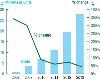
In 2008, e-reader shipments were less than a million units. Semico forecasts sales to grow to almost 30 million units by 2013 with a CAGR of 98.6%. The figure below shows actual shipments for 2008 and forecast unit shipments for 2009 through 2013.

Click to Enlarge
Figure 1. Worldwide e-reader unit shipments. (Source: Semico Research Corp.)

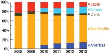
With the majority of e-readers being produced in the Asia-Pacific, the majority of semiconductor revenues are also from that region, though most consumption takes place in the Americas. Throughout the forecast period, the Asia-Pacific will have the largest percentage of revenue, though the Americas and Europe will gain market share with new entrants. Manufacturing done in Japan will move toward the Asia-Pacific, while new manufacturing will start up in the Americas and Europe.

Click to Enlarge
Figure 2. E-reader market share by region.

The earliest e-readers were created in the late ’90s, during a decade of new innovations throughout the handheld market. E-readers offered between 4MB and 16MB of NAND Flash, enough to hold between 10 and 40 e-books. The screens were backlit black & white LCD with some e-readers providing touch screens. To download e-books most devices had to connect to a PC, though a few had a built-in modem. The battery charge lasted about 24 hours.

In 2004, the first popular e-reader was introduced in Japan called the Sony Librie. It was the first e-reader with an electronic paper display (EPD). When e-readers adopted EPDs, the battery life benchmark changed due to the nature of the new screens — EPDs only use batteries when a new page is loaded, instead of LCD screens which constantly use power. As a result, e-readers no longer benchmark their battery life by the number of hours between charges, but by the number of page loads between charging. The battery life for the Librie was about 10,000 pages.

During these years for the developing e-reader market, consumers became accustomed to carrying a cell phone, and an MP3 player, and at times a portable multimedia player (PMP). Only after becoming more accustomed to versatile handheld products were they willing to look into the e-reader market.

It wasn’t until Amazon’s Kindle, released in 2007, that the e-reader finally began to enter the mainstream consumer market. Part of what drew consumers to the Kindle was the ability to immediately download and begin reading e-books anytime, anywhere. Before the Kindle this was nearly impossible. Whispernet, available from Sprint, was another e-ink device that included an EVDO connection, eliminating the need for a PC to download books, though a USB connection was still included. The Kindle had 256MB built-in NAND with an expandable memory slot.

The following figure shows e-reader NAND semiconductor revenue per device.

Click to Enlarge
Figure 3. E-reader NAND revenue in US $M. (Source: Semico Research Corp.)

The next steps for e-readers

The e-reader is no longer a niche product, and has stopped catering to early adopters. The next hurdle for increased consumer acceptance is the price. Currently, the average price hovers around US $300, high enough to turn away many consumers because other types of handheld devices can also read e-books for a much lower price. Penetration rates will dramatically increase once $99 e-readers are introduced.

E-readers on the market today have a screen size between 5" and 11", though this is not a method of identification and may change. Most e-readers aim to mimic the size of a hard cover book or a magazine. The evolution of the e-reader is centered around the e-book content. The main concern for users is having an easy-to-use method of downloading e-books quickly, which is why the Kindle is so popular.

What makes the e-reader device different from other handhelds on the market is its screen, which offers low power consumption and is easy to read in the daylight. E-readers will not be taking market share from other devices — on the contrary, many users will opt to download books onto their small phone or netbook to eliminate the need to buy or carry another device.

E-readers may be subsidized, and usually come with no monthly fee to browse the Web or download e-books, although some devices may limit browsing capabilities and may charge for "shipping" an e-book. While profit margins on e-readers may be low (similar to the gaming market), many manufacturers such as Amazon and Barnes & Noble are banking on revenues from e-book sales as the real benefit. The potential profit in content distribution is much larger than the potential profit of the actual devices.

Future e-readers will include color touch screens and be similar to netbooks, though this is reliant upon the screen technology and how quickly innovations in that market occur.

Breakdown of e-reader technologies

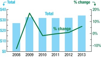
The total semiconductor content value for a typical E-reader in 2013 will be 1.2% higher than in 2009. Note decreases in semiconductor content in 2008, 2010, and 2011. These increases and decreases are due to new entrants to the market and the different features they exhibit.

Click to Enlarge
Figure 4. E-reader semiconductor content. (Source: Semico Research Corp.)

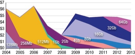
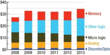
The cost of memory will stay almost constant due to an increase in built-in memory over the years, as well as the sale of SSD cards along with the e-reader. The figure below shows the cost breakout of semiconductor content. (Semico follows SIA category definitions.)

Click to Enlarge
Figure 5. E-reader semiconductor content in US $. (Source: Semico Research Corp.)

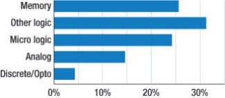
As shown in the following chart, "other logic" has the highest percentage in the semiconductor cost in e-readers for 2009, mostly due to the screen controller. Memory is the next highest percentage, with 25.6% of the total cost. Semico includes a percentage of secondary memory that would be bought along with the e-reader.

Click to Enlarge
Figure 6. 2009 E-reader content by major semiconductor category. (Source: Semico Research Corp.)


Michell Prunty is senior consumer analyst at Semico Research Corp., ; ph 602-997-0337, e-mail [email protected]. For more information on e-readers, Semico offers a free abridged version of an in-depth e-reader report at www.semico.com. To obtain a copy, please contact Sam Caldwell at [email protected] or 602-214-9697.

June 18, 2009 — Carbon Nanotubes (CNTs) and graphene exhibit extraordinary electrical properties for organic materials, and have a huge potential in electrical and electronic applications such as sensors, semiconductor devices, displays, conductors and energy conversion devices (e.g., fuel cells, harvesters and batteries). A new report from IDTechEx brings all of this together, covering the latest work from 78 organizations around the World to details of the latest progress applying the technologies.

Depending on their chemical structure, carbon nanotubes (CNTs) can be used as an alternative to organic or inorganic semiconductors as well as conductors, but the cost is currently the greatest restraint. However, that has the ability to rapidly fall as new, cheaper mass production processes are established, states the report.

In electronics, other than electromagnetic shielding, one of the first large applications for CNTs will be conductors. In addition to their high conductance, they can be transparent, flexible and even stretchable. Here, applications are for displays, replacing ITO; touch screens, photovoltaics and display bus bars and beyond.

In addition, interest is high as CNTs have demonstrated mobilities which are magnitudes higher than silicon, meaning that fast switching transistors can be fabricated. In addition, CNTs can be solution processed, i.e. printed. In other words, CNTs will be able to provide high performing devices which can ultimately be made in low cost manufacturing processes such as printing, over large areas.

They have application to supercapacitors, which bridge the gap between batteries and capacitors, leveraging the energy density of batteries with the power density of capacitors and transistors. Challenges are material purity, device fabrication, and the need for other device materials such as suitable dielectrics. However, the opportunity is large, given the high performance, flexibility, transparency and printability. Companies that IDTechEx surveyed report growth rates as high as 300% over the next five years.

While manufacturers in North America focus more on single wall CNTs (SWCNTs); Asia and Europe, with Japan on top and China second, are leading the production of multi wall CNTS (MWCNTs) with Showa Denko, Mitsui and Hodogaya Chemical being among the largest suppliers. The split of number of organizations working on the topic by territory is shown.

A number of companies are already selling CNTs with metallic and semiconducting properties grown by several techniques in a commercial scale but mostly as raw material and in limited quantities. However, the selective and uniform production of CNTs with specific diameter, length and electrical properties is yet to be achieved in commercial scale. A significant limitation for the use of CNTs in electronic applications is the coexistence of semiconducting and metallic CNTs after synthesis in the same batch. Several separation methods have been discovered over the last few years which are covered in the report, as is the need for purification.

Opportunities for Carbon Nanotube device manufacture

There are still some hurdles to overcome when using printing for the fabrication of thin carbon nanotube films. There is relatively poor quality of the nanotube starting material, which mostly shows a low crystallinity, low purity and high bundling. Subsequently, purifying the raw material without significantly degrading the quality is difficult. Furthermore there is also the issue to achieve good dispersions in solution and to remove the deployed surfactants from the deposited films, according to the report.

September 16, 2008: Nano-C, Inc., developer of nanostructured carbon materials, has been issued US Patent Nos. 7,335,344 and 7,396,520 by the Department of Commerce’s United States Patent and Trademark Office. These newly issued patents cover the manufacture of Nano-C’s core products, carbon nanotubes and fullerenes.

“The fundamental competitive advantage of our technology covered by these patents enables us to offer an array of unique carbon nanotubes and fullerene products, tailored to specific applications,” commented Viktor Vejins, president and CEO at Nano-C . “These technologies provide the needed scalability to meet the growing demands we see in organic photovoltaic (OPV) and electronics applications, including transparent conducting films for use in a variety of display, touch screen and traditional solar applications.”

Executive Viewpoint


August 15, 2008

Shrink the iPhone
By Jim Stratigos, Jacket Micro Devices
Apple’s recently introduced 3G iPhone is a marvel of engineering from just about any perspective; compact, feature rich, cool touch screen, and a plethora of wireless functions. It’s also an indication of how far the electronics industry has yet to achieve in terms of miniaturization of complex analog circuits.

A glance at the single PCB shows about 40 little grey squares of single and multi-die IC packages along with hundreds of discrete SMT components. In fact, many of the little grey squares are SiPs containing IC die and even more passive components. In total, passive components occupy over 40% of the iPhone’s PCB area. What gives? Why haven’t the inductors, capacitors, and filters been absorbed into silicon and put on the Moore’s Law train to sub-micron miniaturization?

The answer is actually quite simple

Particle Counters


July 1, 2008

Compiled by Carrie Meadows

Particle monitoring is an integral part of maintaining adequate cleanliness levels. Here’s a selection of the latest particle counting equipment available.

100 LPM airborne particle counter

Click here to enlarge image

The Biotest APC M3 was the first portable airborne particle counter to sample at a rate of 100 LPM. Measuring 1 m3 of air in only 10 minutes, it cuts the time of particulate air monitoring for its users. When sampling a cubic meter of air, conventional 1.0 cfm (28.3 LPM) units take more than 35 minutes; 50 LPM units take 20 minutes. The APC M3’s higher flow rate reduces the time required to take samples by as much as 70 percent, thereby helping pharmaceutical manufacturers increase productivity and lower labor costs. The counter can also be used with Biotest’s APCOne11–21 CFR Part 11 compliant–Download Utility Software. The software securely transfers data to reduce operator error and meets FDA compliance for data protection. It also has an audit trail to log critical events, password protection features, and digital signature application for authentication of files.

Biotest Diagnostics Corp.
Denville, NJ
www.biotestusa.com

Lightweight counter with reduced emissions

Click here to enlarge image

CLiMET offers 100 LPM sampling with the CI-1053. The airborne particle counter completes a full cubic meter sample in 10 minutes, achieved with a filtered external exhaust that significantly reduces particle emissions. The CI-1053 also incorporates communications capabilities via Ethernet Modbus, TCP/IP, and TELNET. The 14.25-lb particle counter is housed in a seamless stainless steel enclosure, with an internal battery that provides four hours of continuous sampling. The bright touchscreen provides a user-friendly interface. The standard two-year warranty underscores the design, performance, and quality of the CI-1053. This new family of particle counters is also available in similar products with flow rates of 1 cfm, 50 LPM, and 75 LPM. Contact CLiMET for a free demonstration at [email protected] or (909) 793-2788.

CLiMET Instruments
www.climet.com

Remote airborne particle counter for life sciences

Click here to enlarge image

Hach Ultra’s latest MET ONE 6000 Series of remote airborne particle counters features the MET ONE 6015, offering accurate, reliable, continuous particle monitoring for the life science industry. Providing a sensitivity range of 0.5 to 10 µm at 1.0 cfm flow rate, the 6015 is designed to meet the specific needs of cleanroom operations with diagnostic features that provide reduced troubleshooting and downtime related costs. Featuring a wide choice of communication options such as RS-485 Serial Modbus, Ethernet, analog, pulse, and RS-232, the counter is easy to integrate with any facility monitoring system and enables future upgrading as communication needs change. An array of mechanical installation options also reduces downtime related to instrument removal and re-installation during routine calibration and preventative maintenance work. For the life science industry, the device installed with Hach Ultra recommended FMS software such as UVO or enVigil meets the necessary regulatory compliance needs for 21 CFR Part 11. The particle counter can also be integrated with the most commonly used industrial building management system and SCADA software with an OPC server. To request a brochure, send an email to [email protected] or call (541) 472-6500.

Hach Ultra Analytics
Grants Pass, OR
www.hachultra.com

Hybrid handheld particle counter

Click here to enlarge image

Hal Technology (HalTech) has introduced what it says is the world’s first hybrid handheld particle counter, the HPC600 with built-in printer. The HPC600 measures six different particle size distributions simultaneously with sensitivity of 0.3

June 24, 2008Cypress Semiconductor Corp. has introduced the TrueTouch touchscreen solution based on the PSoC programmable system-on-chip architecture. The TrueTouch offering includes a single-chip touchscreen solution that can interpret up to 10 inputs from all areas of the screen simultaneously. This capability, known as “multi-touch all point,” enables designers to create new usage models for products such as mobile handsets, portable media players (PMPs), GPS systems and other products.
Examples of applications well-suited for multi-touch all point functionality include keyboard implementations, inputting multiple locations into a GPS, playing video games on a mobile handset, and making multiple adjustments to sound and/or video settings on a PMP.
In addition to the multi-touch all point products, the TrueTouch family includes devices that perform traditional touchscreen functions including interpreting single touches, and gestures such as tap, double-tap, pan, pinch, scroll, and rotate.
Touchscreens have become the user interface of choice for many applications. Touchscreen technology addresses the conflicting demands for smaller products with larger displays by eliminating traditional buttons without sacrificing screen size. They also enable users to manipulate new functions easily and intuitively by interacting directly with content on the screen. TrueTouch devices support “projected capacitive” touchscreens, which offer numerous benefits over touchscreens based on “resistive” technology. These advantages include optical clarity, durability, reliability and cost-effective implementation of multi-touch features.
“”Leading customers in a variety of markets, including smartphones, GPS and PMP devices, have worked with us to help define the TrueTouch family,” says Dhwani Vyas, vice president of PSoC products for Cypress. “We are leveraging our established leadership in the capacitive sensing markets to deliver the next generation of touchscreen solutions that offer user interface designers unparalleled flexibility and integration capabilities via the PSoC architecture.”
“Our research clearly indicates that projected capacitive touchscreens for consumer electronics devices are poised for strong growth,” adds Jennifer Colegrove, senior analyst, senior analyst and author of the “Touch Screen” 2008 report at market research firm iSuppli. “The TrueTouch family is targeted squarely at this segment.”
Because of the flexible and programmable TrueTouch architecture, customers can choose to work with a wide variety of touchscreen vendors and/or LCD module vendors to create their designs. In addition, the TrueTouch solution utilizes the PSoC architecture’s ability to integrate additional functions such as driving LEDs, backlight control and I/O expansion. These functions, in conjunction with flexible communication options (I2C and SPI), allow for unparalleled system integration for touchscreen systems.