Category Archives: MEMS

by Michael A. Fury, Techcet Group

June 11, 2010 – The 13th IITC (International Interconnect Technology Conference) officially got underway Monday, June 7 at the Hyatt Regency in Burlingame, CA with just under 300 engineers, scientists and technologists in attendance. About 26% traveled from Asia, 12% from Europe and the remaining 62% from the US and Canada, to learn from a program of 43 presentations and 28 posters. Dominant themes this year were variations on 3D and through-silicon vias (TSV), and barrier films for reducing copper electromigration.

Click to EnlargeMark Bohr, Intel CTO, opened the meeting with his keynote address titled "System scaling: The real goal." He’s working on 15nm technology, but limited his discussion to the 45nm products currently in the market. Moore’s Law is continuing, he asserts, but the formula for success is changing. Tight collaboration of process engineers, device designers, and system architects becomes more critical with each generation. Design for low power and portability has fostered adaptive circuitry, in which whole blocks of the microprocessor logic and RAM are switched off when not required. The tolerance for leakage current in mobile electronics is 105 lower than it is for performance computing.

Phil Emma at IBM Research spoke next on "3D systems design: A case for building customized modular systems in 3D." The systems implications for 3D design run beyond the current manifestation that makes things simpler and cheaper. In the near future, 3D will "make things grander;" further out, it will enable us to "make completely new things." These new architectures will be created at the intersection of four basic dimensions in 3D design: packaging density, interconnectivity, modular systems, and heterogeneity.

Hyung Suk Yang of Georgia Tech followed with an example of a 3D interconnect system to provide CMOS signal processing for a large biosensor array. The integration scheme introduces a TSV process that does not require CMP on the MEMS and sensor side of the wafer. It also uses GA Tech’s mechanically flexible interconnect (MFI) design to allow use of disposable sensor units with the drive electronics. The group anticipates that the design will be extendable to meet a demand for up to discrete 50,000 sensor elements on the disposable unit.

A session on Process Integration comprised three papers on self-forming copper barriers, using cobalt (IBM, Albany NanoTech), titanium (Renesas), and manganese (TSMC). In each case, the metal diffuses through the Cu to the surface or sidewall interfaces and functions as the Cu barrier. Each metal gave mixed results as implemented here, but each provided good insights into fundamental mechanisms. Discussions on Co and Mn were underway at RPI under the SEMATECH Center of Excellence (SCOE) in 1988 with Prof. Shyam Murarka — a testament to the incredibly long incubation time for some concepts.

SEE ALSO:

Fourteen papers participated in the poster session, covering the whole spectrum of interconnect issues. I particularly enjoyed Matt Spuller’s description of a PECVD boron nitride material from Applied Materials for use as a dielectric copper barrier and as an etch stop. Compared to SiCN (k=5.1), this BN (k=4.2) shows a 30% increase in breakdown voltage and an 8% improvement in RC delay.

The six-paper session on Materials and Unit Processes was dominated by three CMP talks, two of which were given by Nancy Heylen of IMEC. Scratches in ultralow-k (ULK) dielectrics were found to be caused by silica-Ta and silica-TiN agglomerates about 5μm in diameter that form during the polishing process and persist on the pad surface. The agglomerate formation can be mitigated by modifying the chemical environment in which these elements interact. Her other paper demonstrated the effective use of standard electrochemical methods to discern relative compatibilities of Cu, Ta, RuTa, and Co with five unidentified commercial CMP slurries. This is particularly helpful for resolving galvanic corrosion problems between the Cu and its barrier metal. Mark Oliver from Stanford U. reviewed some molecular design considerations for improving the mechanical properties of ULK materials. Of particular interest is a benzene ring with 1,3,5-Si adducts whose bulk modulus vs. density lies well above the line for homologous C-Si compounds.


Michael A. Fury, Ph.D, is senior technology analyst at Techcet Group, LLC, P.O. Box 29, Del Mar, CA 92014; e-mail [email protected].

June 4, 2010 – Analysts speaking at a breakfast seminar near Boston agree that current chip sales estimates are "conservative" — even after one of them breaks out new optimistic forecasts — and strong demand is pulling the industry back into seasonal trends and more reliable growth patterns.

Gartner’s new forecast, issued this week, pegs 27.1% growth in chip sales in 2010 to $290B, vs. ~20% growth to $276B it forecast back in February. Bob Johnson, VP of research at Gartner, cited a list of factors underpinning the brighter outlook: better PC unit growth (22% vs. 20% in the previous forecast), MPU revenues (14.7% vs. 11%), DRAM revenue (78% vs. 55%), and cell phone units (14% vs. 12%).

Looking further out, it looks like the better 2010 growth comes at the expense of 2011 and 2012, which Gartner now sees as slightly less optimistic — about 1% lower in 2011, and 2% lower in 2012 — Johnson deemed this "a little softness, largely a memory problem." Semiconductor growth is now clearly outpacing not only seasonal norms, but also the broader electronics systems market in general in terms of both inventories and pricing, he noted, and this needs to get back in synch. Look for chip sales to stay on a long-term ~5%/year growth trend.

Click to Enlarge

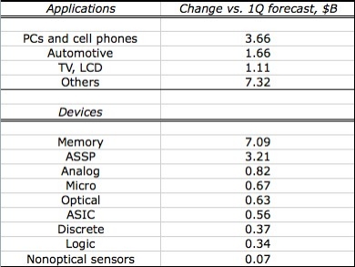
Above is Gartner’s new forecast vs. its old one from February; below is Johnson’s summary of the changes in device type and applications. Note in particular the swing in memory — mostly due to better pricing, not bit demand, he says. This year there are supply shortages across the horizon from memory to analog to foundries, and ASPs and inventories are on the rise; these should all balance again in 2011. And the growth across several applications reveals "a more broad-based demand picture," he said.

Click to Enlarge

That high-20s growth for 2010 might not be enough. Also speaking at the SEMI breakfast near Boston, IC Insights’ Bill McClean said his current outlook of 28% chip sales growth is "conservative," and "can easily go over 30%." The key is underlying strength of demand: in 2009, the worst economic downturn in 63 years, PC units actually rose 1%, and this year could spike to 18% or more — the best in 10 years, he said, now that businesses who bypassed Vista have cash available to spend and are ready to invest in Windows 7 machines. He also pointed to a return to trending for IC unit shipments at around 9%; some inventory buildup (e.g. in analog and special logic) "won’t be a problem if we stay on a seasonal trend," he said.

Semico analyst Jim Feldhan likewise called his own 27% growth number for 2010 conservative; "I can see a little above 30%, if memory pricing holds." Like Gartner he sees a mild slowdown in 2012, and mid single-digit growth in 2013-2014. He noted that of ~45 end markets Semico tracks, the semiconductor content continues to get richer, and a younger generation of users sees these beefier devices with better technology as a necessity, not a luxury. Communications infrastructure will be a driving force in the next several years, as will an upgrade cycle for PCs and phones, including more robust varieties — "the Chinese are just as interested in smart phones as the rest of us," he said. Solar applications are becoming important, not just the base silicon but also systems, e.g. inverters and "smart grids." And an even auto is an increasingly key market — the US now sells 2M fewer cars that its estimated replacement level, he pointed out, so a catchup in this sector helps devicemakers from MEMS to infotainment.

By Jerôme Baron, Yole Développement

May 24, 2010 – It’s not just 3D packaging technology where CMOS image sensors are driving IC technology these days. Ultrathin silicon that enables back-side illumination (BSI), and integrated wafer-level optics are bringing sharply improved performance, lower costs, and smaller size, driving CMOS image sensors into more and more markets — and these technologies may soon impact other IC manufacturing as well.

Thinning silicon wafers down to 5μm transparent films to let light through the back side is driving a 2× to 5× improvement in sensitivity for smaller pixel image sensors. Yole Développement sees CMOS sensors now moving quickly into higher performance applications, including high resolution digital SLR cameras and digital video recorders, as they come to match the performance of CCDs at lower cost. These thinning and annealing technologies may also open new possibilities for 3D stacking and integration of very thin layers of memory and logic devices in the future. Wafer-level optics are also starting to reduce camera module size and cost in even demanding handset applications, and could also bring similar improvements to projection lens systems for gaming stations and micro displays.

CMOS image sensors drive ultrathin wafer technology roadmap

One of the key breakthroughs that enables these major improvements in performance and price is backside illumination, which requires thinning the silicon wafer down to a transparent 5μm active layer, so the light can come in directly to the photo diode from the backside. Putting the electrical distribution layers behind the photo diode allows a simpler and more flexible BEOL architecture design, eliminating the need to leave openings in the pattern to let light through, and naturally lets in much more light, allowing higher resolution or higher sensitivity for the same given sensor size and cost. Next step, now in the development stage, is to take advantage of this increased design flexibility and add more intelligence to the system, by stacking a microprocessor DSP below the sensor — moving towards the ideal of controlling each pixel individually as in the human eye, for much improved sensor performance across different light conditions.

Click to Enlarge
Figure 1. Example of CMOS BSI "SOI" process flow. (Source: Yole Développement, "CMOS Image Sensors: Technology and Markets 2010")

The BSI process flow starts with making the photo diodes. Then the device wafer is bonded at low temperature to a silicon or glass carrier, using either adhesive polymers or molecular oxide-to-oxide bonding. US-based 3D-IC company Ziptronix offers one low-temperature bonding solution, which presses together ultraflat wafers, well prepared through specific surface preparation treatments. Next, the 1mm thick photo diode wafer is thinned down to 40-50μm with Disco or Accretech grinding tools, then thinned further with CMP, and finally etched down to an etch-stop layer at 5μm. This radical wafer thinning typically requires precise control of wet etching after initial grinding and CMP. One option, used by Sony and others, is to use SOI wafers from Soitec, using the buried oxide layer as an inner etch stop layer at the oxide interface — though the high cost of SOI wafers may limit the process to high-end imaging applications only. Others, including OmniVision, working with TSMC and Xintec, claim to have developed a lower-cost alternative process using bulk silicon wafers with graded implant layers. The trick is to find a highly selective etch chemistry that will stop precisely at the required 5μm thin silicon interface, just before reaching the photodiode structures.

Also critical is the annealing process, since this 5μm thin silicon film needs to include a very narrow implant gradient, to prevent recombination in the epi silicon and to push the photons down to the photo diodes. Since typical annealing ovens can only be controlled to about 30μm layer precision, the finer implant gradients require annealing with a nano-second, local heating laser process. The French equipment company Excico supplies a tool that uses a UV excimer type of laser source with a large spot for tight precision with better image quality and higher throughput.

This ability to build and handle these ultrathin layers also opens new possibilities for 3D stacking and integrating very thin active layers monolithically on top of other semiconductor applications. Indeed, such type of process set-up has the potential to be re-used in the future for 3D integration of memory + memory, logic + memory or MEMS + logic applications.

Coming next: Wafer-level integration of optics

The next development just starting to impact the CMOS image sensor business is wafer-scale integration of the optics, to drastically reduce size and cost, and to simplify the assembly process and supply chain. The camera module unit remains one of the largest components in most cell phones, and among the most complex to manufacture, requiring sourcing and assembly of up to 15 different components, including not only lenses, but also IR filters, caps, barrels, spacers, autofocus mechanisms, and other parts. An attractive alternative is wafer-level processing of optical lenses, today already in low-volume production by Heptagon for STMicroelectronics and by Anteryon for Toshiba camera modules.

Click to Enlarge
Figure 2. Wafer-level camera module assembly steps. (Source: Yole Développement, "CMOS Image Sensors: Technology and Markets 2010")

A typical wafer-level optic process involves dropping a polymer layer on to a glass wafer, pressing in the desired pattern through molding and UV replication with nanoimprint lithography tools, to imprint some 4000 lenses at once on each 8-in. wafer. This wafer is then aligned and bonded to another lens or spacer wafer, then tested and finally diced into small, low-cost optical lens camera-module cubes.

Companies are also working on integrating autofocus functions at the wafer level. A number of players, including SEMCO, are working on electro active polymers, whose thickness can be controlled and driven electrically by applying a defined voltage. Others like Siimpel (recently acquired by Tessera) have a MEMS- based solution, using a spring-like silicon structure.

But the front-runner currently appears to be a potentially breakthrough technology using liquid crystal polymers. The startup LensVector plans to start production this year of a four-layer stack of 8-in. glass wafers, encapsulating liquid crystal polymers that change shape when voltage is applied to the driving electrodes — all in less than 500μm total thickness. This technology has the potential to significantly bring down the size and cost of camera modules in the future.

These increasingly integrated optics will likely find application in other products as well, to simplify the manufacture and reduce the size and cost of other optoelectronics, across applications ranging from biomedical endoscopy to consumer products like digital cameras, pico projectors, headsup automotive displays, projection systems for gaming, and LED lighting.

Wafer-level packaging moves to higher-performance devices, more applications

Image sensor makers were among the first to move to volume production of wafer-level packaging and through-silicon vias (TSVs), as the technologies offered a solution to the big yield losses from the complex demands of alignment in packaging and assembling the optics with the high cost sensor chips into plastic modules. From initial use of Tessera’s ShellcaseOP glass-capping technology with low-end CIF and VGA format single megapixel camera units, the WLP technology has moved upstream to more complex and finer pitch devices up to 2-3 megapixels. TSMC’s Xintec packaging unit is currently running more than 200,000 8-in. WLPs a year, mostly for OnmiVision. Toshiba, Samsung, and STMicroelectronics are producing internally in volume. Considerable MEMS volumes, and some LEDs and memory chips as well, are also starting to use similar technology as the infrastructure builds up worldwide and costs come down with volume.

Click to Enlarge
Figure 3. CMOS image sensors technology drivers — new challenges to face. (Source: Yole Développement, "CMOS Image Sensors: Technology and Markets 2010")

Jerôme Baron tracks MEMS and advanced packaging technologies and markets at Yole Développement. He recently authored the report "CMOS Image Sensors: Technology and Markets 2010".

(May 17, 2010) LYON, France — An IC foundry has made it into the ranks of the Top 20 MEMS foundries for the first time, as TSMC’s roughly $10 million in MEMS foundry revenues put it into 14th place on Yole Developpement’s 2009 listing. STMicro improved slightly, continuing to dominate the MEMS foundry arena. TI slipped, holding onto #2; Dalsa gained, and grabbed the #3 slot.

Click to Enlarge
TOP 20 MEMS Foundries – 2009 revenues.

In 2010, STMicroelectronics continues to dominate the MEMS foundry business, with some 40% share, up slightly in 2009, as its revenues held up significantly better than most of the other major foundries in the downturn in consumer electronics and automotive sales. Healthy 19% growth pushed Dalsa Corp. past Micralyne Inc. to become the largest of the pure-play MEMS foundries with $31 million in revenues. Dalsa moved into third place overall, closing the gap with number two Texas Instruments (TI), who saw its foundry business slip 24% last year to $45 million. Perennial MEMS market leaders TI and Hewlett Packard (HP) were the top overall MEMS suppliers in 2009, although they were no longer dominant in the market like in the past.

Foundries continued to gradually take a larger share of total MEMS production, with total foundry revenues at the leading companies holding up somewhat better than MEMS sales overall. Top 20 foundry revenues, which account for the vast majority of the foundry business, declined about 3% in 2009, slightly less than the roughly 5% drop in MEMS sector revenues overall.

Asia Pacific Microsystems (APM) and Touch Microsystems (TMT) rode the Asian growth wave to 17% and 29% increases in sales, respectively. Jazz Semiconductor saw 25% growth, as startups started production of some new MEMS applications.

HP is now the largest customer for MEMS foundry services, as the inkjet nozzle maker pursues a fab-light strategy. InvenSense and Knowles Electronics follow as the next largest users, and the first companies to make a significant success — with revenues of more than $80 million — using the fabless model to build a business in innovative MEMS products, with their low-cost consumer gyroscopes and sector-leading MEMS microphones, respectively.

IC companies with their available 8″ fab capacity will continue to make inroads in the MEMS business, as they master different MEMS product technologies and figure out how best to manage the multiple different process flows. Meanwhile the specialty MEMS foundries — all still under $35 million in annual sales, and most much under that — have to figure out how to afford advanced production technology for larger volumes, at consumer product margins. That may leave foundries focusing on a bimodal distribution of tasks — doing, on one hand, the more standard volume manufacturing of mainstream technology that is not key to product differentiation, and on the other hand doing the development of the most sophisticated leading-edge devices where specialized manufacturing experience can provide faster time to market.

More of the big IDMs that dominate the MEMS market are also offering or using foundry services to make most efficient use of their capital investment. MEMS makers from Sony to GE Sensing and Olivetti are offering their production services to select outside customers to help fill their fabs. Even Robert Bosch has restarted offering limited foundry services in its fab, helping companies with prototyping and running multi project wafers — as long as customers use Bosch technology blocks without customization.

Meanwhile, other MEMS producers are turning to external foundries instead of adding or updating their own captive capacity. Yole figures another five major MEMS systems makers are now looking to use external foundries, which will boost the foundry business by some $350 million.

Read the 2009 MEMS suppliers report from Yole.

For more information, visit www.yole.fr

(May 13, 2010) ELK GROVE VILLAGE, IL — As part of its bonded wafer inspection technology, Sonoscan demonstrated acoustic imaging of defects in the seal that surrounds and protects the cavities in MEMS devices.

Click to EnlargeThe defects most frequently take the form of voids (Device 1) within the seal, Click to Enlargewhich may be direct silicon (Si), metallic, glass, or polymer, depending on the reliability level of hermetic seal required as per SEMI MS8-0309. In some locations on a wafer, the seal may be breached (Device 2). Another frequent defect is delamination of the seal from one or both substrates, the result of poor wetting or contamination during fabrication.

The defects are risky because thermal and mechanical stresses can cause them to grow until they result in a leak in the seal and subsequent loss of the desired cavity atmosphere. The seal prevents outside particles, gases, and humidity from reaching the cavity. Humidity, for example, can result in freezing up of moving parts within the cavity.

Defects in the seal may be only a few tens of microns in diameter and of submicron thickness, but can be imaged by Sonoscan’s C-SAM systems because they represent a gap that reflects >99.99% of the VHF/UHF ultrasonic pulse.

In production, a percentage of MEMS devices may be imaged with C-SAM acoustic micro imaging systems to verify that process parameters are preventing the formation of voids. Where high reliability is essential, as in mil/aero or medical MEMS, 100% of devices may be inspected.

For more information on inspection services, contact SonoLab manager Ray Thomas at (847) 437-6400 x245. For more information on inspection systems, contact Sonoscan’s technical marketing manager Steve Martell at (847) 437-6400 x240.

The images show Sonoscan acoustic images of voids (Device 1) and a breached seal (Device 2) in MEMS devices before wafer dicing.

by Neha K. Choksi

May 12, 2010 – Optical lithography methods are expensive, lack flexibility, and lack resolution for the sub-50nm node. Nanoimprint lithography (NIL) is considered an attractive alternative. NIL is a method of patterning in which a three-dimensional surface pattern of a stamp is transferred onto a moldable surface film on a substrate through mechanical contact. The resulting 3-dimensional pattern on the surface coating is then transferred to the underlying wafer by common semiconductor processing techniques.

Most imprint lithography vendors use spin on tools to create a 50nm thin-film surface coating before embossing. Molecular Imprints, however, has a different approach: Jet and flash imprint lithography (J-Fil). S.V. Sreenivasan, founder and CTO of Molecular Imprints, shared the company’s approach with attendees at the IEEE San Francisco Bay Area Nanotechnology Council seminar on April 20, 2010.

Because real world applications of nanolithography entail pattern complexity and density variations at both the macro and micro scale, this technique deposits the surface coating where it is most needed on the substrate by leveraging standard inkjet technology (see figure). After low-pressure embossing, the resist is UV cross-linked before the mask is separated from the surface, eliminating the use of solvent. The mask makes contact in the middle of the field with radial sweeping action to minimize bubble formation.

The key to this inkjet deposition method is a low-viscosity monomer resist and the use of small volume droplets (on the order of 1.5pL). Because the droplet density can be tailored to the desired pattern density, the fluid travels less distance during the stamping process. Also, the use of this "drop on demand" technique reduces the thickness and the variation of the residual layer that is inevitably left on the lower surfaces of the 3-D resist imprint. This reduces overall non-uniformities of the final pattern. The inkjet tool itself must be carefully calibrated, as variation exists even between same inkjet models.

Click to Enlarge
Step-and-flash imprint lithography process. Benefits include throughput (room-temperature process) and lower capital cost (no track system). (Source: Molecular Imprints)

The company is careful to control the surface energy of the mask. The need to keep the surface energy low enough to allow easy release of the mask from the resist, but not so low that the mask surface itself will not consistently wet, must be carefully controlled. Initially, this technique leveraged a stepper technique for imprinting — the precise fluid deposition reduces the edge bead challenges enabling successful stitching of fluid fields. However, the company now has the option of whole substrate printing as well.

By leveraging its NIL technique for a variety of applications, the company aims to be a market leader in the field. Because the cost-sensitive magnetic storage industry requires a high-density of precise islands of magnetic material separated by non-magnetic material, their high-resolution, low-cost patterning technique of NIL is an attractive solution when compared to the costly 193nm optical lithography method. The company has also demonstrated 2.55nm linewidth roughness and 18nm half-pitch using their stepper patterning technique for non-volatile memory applications. In this case, NIL can be mixed and matched with mainstream photolithography to achieve the associated critical dimensions where necessary.

Furthermore, researchers at the University of Texas are exploring the use of NIL technology for biomedical applications. By leveraging the J-Fil technique to create well-controlled dot structures, researchers are able to study the impact of particle shape, aspect ratio, and size on the effectiveness of particles for targeted nanoparticle drug delivery to fight lung cancer. Because the process selectively deposits the material before patterning, the material waste is less than that of spin or roll-on techniques. This enables a lower cost per dose when compared to other techniques.

Despite its success, Sreenivasan concedes that imprint lithography is not yet ready for all applications. For example, silicon microprocessors have a low tolerance for defects thus making it an unlikely fit at this time. Regardless, Sreenivasan is optimistic that the company’s non-traditional approach to NIL will enable it to further lower cost and reach 10nm feature sizes for production solutions on the horizon.


Neha K. Choksi is an independent consultant based in Mountain View, CA. She has worked for a variety of MEMS companies including as director of product engineering at Silicon Microstructures and as a consultant focusing on commercialization and high volume production of MEMS devices. E-mail: Choksi [at] gmail.

May 12, 2010 – Researchers have come up with a way to calculate and manipulate the effects of Casimir forces, and then use them to keep microelectromechanical systems (MEMS) components from sticking together, which could greatly reduce failure rates and enable new, more affordable devices.

Casimir forces, discovered more than 60 years ago, are quantum forces affecting objects at miniscule distances. At such tiny dimensions, a number of particles flash in and out of existence, with interactions that generally balance out — but at extremely close distances Casimir forces apply to attract particles together. In the 1960s researchers figured out a formula to theoretically describe the effects of Casimir forces on tiny objects, but stopped short of actually solving and evaluating such interactions except for a few examples (e.g. two parallel plates, or more recently a plate and cylinder).

Now, researchers from MIT say they have come up with a way to solve Casimir-force equations for any number of objects with conceivable shape. Their work is published in the Proceedings of the National Academies of Sciences (PNAS). Essentially, effects of Casimir forces on objects <100nm apart can be precisely modeled using objects both 100,000× bigger and further apart that are immersed in a conductive fluid, by calculating the strength of an electromagnetic field at various points around the objects.

"Analytically, it‚s almost impossible to do exact calculations of the Casimir force, unless you have some very special geometries," according to Diego Dalvit, a specialist in Casimir forces at the Los Alamos National Laboratory, in a statement. In principle, the technique, however, "can tackle any geometry. And this is useful."

Very useful, in fact, for MEMS devices, where attractive Casimir forces can cause moving parts to stick together and stop working properly. Earlier this year, the MIT researchers in collaboration with Harvard described an arrangement of materials that enable Casimir forces to cause repulsion in a vacuum. MEMS device design would still require intuition of certain geometries and their properties, though, to know where such repulsion could occur, Dalvit notes.

Note that last year a Harvard-led group examined Casimir forces and how to change the attractive force into a repulsive one — but that work focused on known repulsion for objects in fluids, while the new MIT-led work is about the unexplored area of vacuum-separated objects, explains MIT paper’s lead author Alex Rodriguez. "The ability to obtain Casimir repulsion between vacuum-separated objects was not known and is the subject of much on-going research in this field — as a matter of fact, many scientists believed it was impossible, including myself," he tells Small Times.

Click to Enlarge
Though negligible at larger scales, Casimir forces can cause moving parts of micromachines to stick together. (Image: Sandia National Laboratories, MIT)


May 11, 2010 – Researchers from Georgia Tech and the National Institute of Standards and Technology (NIST) have developed methods to more accurately measure the length of nanopores in membranes, seen as a first step in calibrating tailor-made versions for applications such as rapid DNA analysis.

Single-nanometer-scale pores in thin membranes could act as "miniature analysis labs" for detecting and characterizing biological molecules, e.g. DNA or toxins, as they pass through or block the passage. Such systems could fit on a microchip (e.g., microfluidics — with more precise knowledge of the nanopore’s dimensions and structural features.

Their work, described in the Journal of Chemical Physics, involved drilling nanopores into a bilayer sheet of lipid molecules similar to membranes found in animal cells. Applying voltage across the membrane wall forced charged molecules (e.g., single-strand DNA) into the nanopore; as it passed into the channel, the ionic current flow reduces for a time that is proportional to the size of the chain — thus, its length can be derived.

The scientists also developed two ways of measuring these nanopores.

If a chain is long enough to reach the nanopore’s "pinch point," the force of the electrical field behind it will push the molecule through the rest of the channel. Exploiting this feature, the scientists developed a DNA probe method to measure distances from the openings on either side of the membrane to the pinch point — and adding them together gives the entire length of the nanopore. The probe method involved DNA strands of known length with a polymer sphere on one end; the aforementioned force that would push the strand through the pinch point now lodges the sphere in place with the DNA chain extending into the channel, and defines the distance to the pinch point. (If the chain is shorter than the pinch-point distance it is bounced out of the nanopore.)

Another way they devised to measure the length of the nanopore is dubbed the "single lollipop" method. Polymer molecules circulating in the solution collect on the inner side of the membrane; polymer-capped DNA probes of different length are forced one at a time into the nanopore from the opposite side. Probes with a DNA chain long enough to traverse the entire channel will affix to a free polymer molecule, thus defining the channel’s length. This "ice fishing" method also provides insight into the nanopores’ structure, by mapping the DNA chain’s voltage changes to the changing shape of the channel as it winds its way through.

Click to Enlarge
How the "ice fishing" method determines the distance across a membrane nanopore. DNA strands of known lengths topped by a polymer cap (orange sphere) are driven through the nanopore. Strands long enough to completely transverse the channel (left) will "hook" a circulating polymer (green sphere) on the other side of the membrane, and define the nanopore’s length. If not long enough, the DNA probe will bounce out of the pore (right). (Credit: J. Robertson, NIST)

April 21, 2010 – Mitsubishi Heavy Industries (MHI) says it has delivered its first automated room-temperature bonding system for 200mm wafers to a MEMS manufacturer in Japan, the tool‘s first use in production.

The company’s MWB-08A tool incorporates a 20-wafer cassette (10 pairs) with fully automated wafer transfer and alignment. Bonding conditions are programmed for each wafer set, offering flexibility for small-lot production of various products. The tool’s functionality is compatible with earlier 150mm machines, so an upgrade path is available.

The tool transfer also includes MHI’s "Bonding Support Program," which liaises the company’s engineers and facilities with the customer to help support device development in applying room-temperature wafer bonding at each development stage: from conceptual design to functional prototype production to trial and mass production.

Room-temperature bonding activates the substrate surface with ion beam irradiation in a vacuum. Conventional wafer bonding applies heat; eliminating this step removes heat stress and strain, enabling rigidity and reliable bonding, and reduces cycle time (no heating/cooling cycle), the company explains. The end result is "significantly shorter production time," higher yields, and ultimately lower device production costs.

by Michael A. Fury, Techcet GroupClick to Enlarge

April 16, 2010 – The fourth day (Thurs. 4/8) of the MRS Spring 2010 meeting in San Francisco was another full agenda of parallel sessions, although my reporting on the day is somewhat abbreviated. Highlights included: through-silicon vias (TSV) and flexible interconnects; 300mm BCB wafer bonding; carbon nanotube interfaces for interconnects and vias; phase-change memory devices; interfaces during atomic-layer deposition (ALD) of rare earth-based high-k dielectrics; and graphene as a key material for on-chip interconnects and transparent conductor electrodes.

(Underscored codes at the beginning of papers reviewed refer to the symposium, session and paper number; additional presentation details can be found in the MRS Spring 2010 program.)

F9.1. Muhannad Bakir at GA Tech showed a novel through-silicon via (TSV) approach for 3D CMOS and MEMS integration using mechanically flexible interconnects. The performance of many MEMS devices depends on mechanical stresses, which must not be perturbed by the packaging integration to CMOS devices. This work uses a mechanical flex interconnect (MFI) in place of solder balls to relieve the TCE mismatch stresses between the MEMS and CMOS devices. Fabrication uses a reflowable sacrificial polymer to form a dome, over which Cu is electroplated. After removing the polymer, the Cu structure provides a 20μm standoff with solder balls deposited on the tips. The new TSV process is designed to avoid CMP and any potential damage to the MEMS devices, and employs a perforated back-side oxide stop layer in which the etched holes are first plated over with Cu from the back side, filled with Ni from the front side, and then the via is filled with Cu from the front side. Finally, the oxide stop layer and Ni plugs are stripped from the back side.

Other MRS blog entries:
Day 3: Nanoimprint litho, 32nm memories, FET/Si/CNT sensors
Day 2: CVD for Cu, low-k etch stop, future FETs, graphene "atom hopping"
Day 1: Charge-trapping NVM, organics, graphene, PV

F9.6. Pratibha Singh of GlobalFoundries presented an optimized 300mm BCB wafer bonding process for 3D integration, capable of supporting 400°C Cu-Cu thermocompressive bonding. An important element of this process is a hard bake to crosslink the BCB prior to bonding, which is critical to avoid dendrite and void formation.

F10.3. Mark Strus at NIST described a reliability investigation of carbon nanotube (CNT) electrode contact interfaces for interconnect and via applications, using individual multiwalled carbon nanotubes (MWNT) welded to a Ni probe. For Cu contacts, both resistance and temperature rise as the voltage increases. For CNTs, the temperature decreases as the voltage increases, until just before a catastrophic failure. Details of the failure mechanisms are different for AC and DC testing modes.

F10.4. Bin Yu at Albany CNSE investigated some key reliability limits for on-chip interconnect applications of multilayer graphene systems. The mobility of graphene is 20× higher than Si and its thermal conductivity is 10× higher than Cu, making it an attractive design and fabrication material. The electronic structure is different for mono-layer, bi-layer, and tri-layer graphene; bi-layer graphene (BLG) was studied here due to its controllable band-gap tenability. BLG has a breakdown current density of 108A/cm2, 100× greater than Cu. The data suggests Joule heating as the primary breakdown mechanism.

G14.1. Ilya Karpov of Intel presented some characteristic behaviors, physical models, and key materials properties of Ge2Sb2Te5 (GST) phase-change memory devices. Device operation requires >1V gap between the set and reset threshold voltages, Vth, which are dependent on a critical field strength. This Vth is proportional to the thickness of an amorphous layer atop the GST device element. In the device configuration discussed, the amorphous-crystalline phase change is driven by the field strength, not by temperature. The physical limit for read speed is ~1ps, which is the lag time for the phase change after voltage switching, which occurs without diffusion.

I3.6. Luca Lamagna at Laboratorio MDM in Italy described the evolution of interface properties during atomic-layer deposition (ALD) of rare earth-based high-k dielectrics on Si, Ge, and III-V substrates. Runaway surface oxidation can be prevented during the early stages of deposition by use of process conditions that promote an interface passivation layer. Close study of the deposition mechanisms shows that the film thickness evolution can be separated from the growth rate evolution. The combination of substrate properties and ALD process parameters has a strong influence on the interface structure and subsequent film growth.

S10.1. Rodney Ruoff at UT Austin talked about his work on the science and applications of graphene-based materials. Free-standing sheets were fabricated by growing graphene on Cu foil (1000°C at 500 mTorr, 35 sccm CH4 in H2). The graphene is then coated with PMMA, the Cu is dissolved in acid, then the PMMA is dissolved in acetone. The graphene growth mechanism was explored in detail by alternating C12H4 and C13H4 in the inlet gas. Preliminary characterization results suggest that graphene may become competitive with ITO for transparent conductor electrodes.


Michael A. Fury, Ph.D, is senior technology analyst at Techcet Group, LLC, P.O. Box 29, Del Mar, CA 92014; e-mail [email protected].