Category Archives: LEDs


Executive Overview

As the semiconductor industry continues to push for smaller chip footprints on larger wafers, it becomes even more important to be able to inspect wafers and detect defects as quickly as possible. The capabilities of advanced motion controllers can give OEMs a distinct advantage in being able to achieve these demands by centralizing all automation control. In this article we will discuss how semiconductor OEMs can increase performance and reduce costs by utilizing advanced motion control techniques and diagnostic tools that are available today.

Cameron Sheikholeslami, ACS Motion Control, Eden Prairie, MN, USA

An OEM of high precision electron beam wafer inspection machines recently identified three core needs in their next generation machine: 1) High-resolution position feedback, 2 Extremely tight position standstill and constant velocity jitter, and 3) The ability to easily interface with both Windows and Unix-based PCs.

Cost constraints and the requirement for minimum time to market led this OEM to choose a control system solution composed of standard off-the-shelf components, configured specifically to meet the application needs.

The OEM’s need for extremely high-resolution position feedback devices was crucial. Previous generation machines had been utilizing standard linear encoders, however, these devices are limited in their accuracy for resolving position. For example, a 20µm linear scale analog encoder with 12-bit resolution can only be resolved to around 4.88nm. Linear encoders are also buried inside a position stage, which means that while they accurately detect the position of the motor, they introduce an error when the goal is to know the position of the load. This error is negligible for many applications, but relative to the accuracy requirements of the OEM, it can quite large.

Laser inferometer feedback

To address these issues, the OEM decided to use laser interferometer feedback devices on the next-generation machine. Laser interferometers are the ultimate feedback devices for high-precision motion control applications because of their ability to determine position with extremely high resolution. In this application, a He-Ne laser with a wavelength of 632nm was used with 12-bit resolution that is accurate to around 0.04nm. Also, they can measure the position directly at the load, which removes a source of error that the linear encoders introduced.

Certain limitations of the laser interferometers cannot be avoided. One limitation is that the interferometers are strictly incremental devices with no "home" reference point, which can cause problems in zeroing the machine. A second limitation is that while measuring the position at the load increases accuracy, it also reduces servo bandwidth and stability, especially with stages that are not very stiff. This is because the structure resonances have a phase lead characteristic when the feedback is close to the motor (which can be easily tuned), while the structure resonance has a phase lag characteristic when the feedback is close to the load, which is more difficult to tune. A Bode plot from an actual system is shown in Fig. 1 and depicts the different frequency response when the laser feedback and encoder are used (plotted in a dashed and bold line, respectively).

Figure 1. Bode plot of a laser interferometer depicting the different frequency response for when the laser feedback and encoder are used.

The motor commutation is not as accurate for the same reason. A third limitation is more cost related, but relates to the mirrors. Shorter mirrors reduce cost, but they also reduce the total range of travel. In the same regard, it is also easy to block the laser beam and lose feedback, which is problematic if the motor is moving fast and friction is low, as disabling the axis may cause the motor to run into the hard stops.

Figure 2. A dual feedback scheme using laser interferometers and linear encoders.

To get all the benefits of the laser interferometer without suffering from the limitations, the OEM ultimately decided on using a dual feedback scheme that employed both the laser interferometers and the linear encoders (Fig. 2). The MC4U is designed such that the OEM was able to run the machine in single-loop mode with the encoder feedback, single-loop mode with the laser interferometer feedback, and dual-loop mode with the laser interferometer providing the position feedback, and the encoder providing the velocity feedback (all modes use the linear encoder for commutation). Also, on-the-fly switching allows the user to switch between modes at any time, even if the motor is in motion.

There is no issue with homing because the linear encoder index is sufficiently accurate and repeatable to set the reference position for both the linear encoder and laser interferometer. The advanced tuning tools available from the MC4U address the tuning difficulty, and the ability to change the tuning parameters on the fly allows for an easy transition between the different feedback modes. There is no issue with motor commutation because it is always updated using the linear encoder. The short travel range and safety issue that could occur if the laser beam is blocked is addressed by the on-the-fly switching of the feedback so that if the motor moves beyond the travel range or if the controller loses the interferometer feedback because of a beam block, it simply reverts to the single loop mode using the linear encoder.

Figure 3. A comparison of performance when using encoder feedback vs. the laser interferometer feedback. After 0.27s, the feedback source is changed from the encoder to the laser interferometer. The plot shows the stage position error while at standstill, with the y-axis units of 10nm per division.

A comparison of the performance when using the encoder feedback versus the laser interferometer feedback can be seen in Fig. 3. This figure is a plot of the stage position error while at standstill, with the y-axis units of 10nm per division. At the beginning of the plot, only the encoder feedback is used, which gives reasonable position jitter of around +/- 20nm. Around 0.3s into the plot, the on-the-fly switching from single-loop encoder mode to single-loop laser interferometer mode is activated and the position jitter significantly reduces to <+/- 5nm.

The tuning tools used by the OEM included the frequency response function (FRF) analyzer, a tool that generates a Bode plot representation of the system response. This powerful tool allows the OEM to accurately determine the electro-mechanical signature of the system (i.e. transfer function), which enabled them to put in appropriate filters to handle the phase lead / phase lag resonances introduced by the location of the feedback device.

Advanced motion control systems can help enable automated wafer transport systems to streamline a semiconductor manufacturer’s production and increase the capacity of fabrication lines. Often these systems employ specially-designed robots with minimal weight and footprint, traveling on a linear translation stage to transport wafers from one location to another.

  1. Typically, the main design challenges of a control solution for such systems are:
  2. Real-time kinematic calculations. The coordinate system of the moving motors is different from that of the moving wafer. The controller needs to calculate in real time the complex equations that translate the required movement of the wafer to the movement of the motors.
  3. Minimizing cabling of the moving robot arms while keeping weight at a minimum.
  4. Scalability: the ability to add axes and I/Os without affecting the basic solution.

For systems with such constraints, a fully-integrated controller topology is not ideal because of the many long, heavy cables required to connect the motors to the integrated controller and drive chassis. Long motor cables are especially susceptible to EMI noise and can significantly degrade overall control performance. Instead, a fast EtherCAT network topology (other networks, such as CANOPEN or DeviceNet, cannot meet the required network communication throughput) with a small form factor master controller housed in the main control chassis and small lightweight drives placed directly on the moving robot, provides an optimal solution. The only cable required between the master controller and the slave drives is the EtherCAT communication cable, which is not sensitive to EMI and is insignificant in terms of weight and drag to the moving system. This solution is also scalable, making it simple to add additional axes of drives or I/O modules for various models of the transport machines.

Conclusion

The recession has placed significant cost constraints on the entire IC fabrication process, placing the onus on OEMs to cut costs on inspection equipment while still exceeding the performance capabilities of previous generation machines. The capabilities of advanced motion controllers enable OEMs to centralize all automation control and achieve high-performance requirements. Motion control systems not only provide semiconductor OEMs with increased performance, but they can also reduce costs by utilizing off-the-shelf components as well as advanced motion control techniques and diagnostic tools.

Biography

Cameron Sheikholeslami received his bachelor’s in electrical engineering and biomedical engineering from the U. of Minnesota, Twin Cities, and is a control and applications engineer at ACS Motion Control, Inc., 6575 City West Parkway, Eden Prairie, MN 55344 USA; ph.: 763-559-7669, x132; email [email protected].

More Solid State Technology Current Issue Articles
More Solid State Technology Archives Issue Articles

Click to EnlargeIn an exclusive series of blogs, imec reports from its International Technology Forum (ITF) last week in Brussels. Els Parton, science editor, imec, shares Jy Bhardwaj’s (Philips Lumileds) points about LEDs costs improvements.
 
May 31, 2011
— LEDs currently appear in applications where performance — color, brightness, light quality — defines a compelling advantage over conventional light bulbs. A few barriers still stand between LEDs and mass adoption in illumination. "First, there is the cost (lumens per dollar) that has to decrease by a factor 10 if LEDs want to be competitive with conventional bulbs. This 10x cost reduction will be achieved by both performance and cost improvements. More in detail, this will be achieved by increasing the internal quantum efficiency (IQE) at high drive current, by improving the Phosphor conversion and by increasing the wafer size with yield and scale enhancement," Jy Bhardwaj, vice president technology R&D at Philips Lumileds Lighting Company, explains.

The second barrier to be overcome is light quality, states Bhardwaj. How do you achieve a consistent, controllable shade of white? An important research topic to tackle this problem is getting a good control of the phosphorous layer (density and thickness) in the LED stack. "Our company has come up with a new device architecture that enables this. It’s a thin film flip chip architecture for InGaN LEDs,"explains Bhardwaj.

Bhardwaj predicts that it will take another 3 years to achieve the desired 10x cost reduction. And by 2020, 80% of our planet’s lighting will come from LED.

Bhardwaj’s colleague Iain Black at Philips Lumileds recently spoke to Solid State Technology’s The ConFab audience about LED manufacturing improvements. Read his points about LED costs improvements via manufacturing here.

Els Parton, science editor, imec, and colleagues are blogging exclusively for Solid State Technology and its ElectroIQ.com partners from imec’s International Technology Forum (ITF) last week in Brussels.


Read more blogs from imec’s ITF:


Subscribe to Solid State Technology/Advanced Packaging.

Follow Solid State Technology on Twitter.com via editors Pete Singer, twitter.com/PetesTweetsPW and Debra Vogler, twitter.com/dvogler_PV_semi.

Or join our Facebook group

May 31 2011 — RJR Polymers, high-performance air cavity package (ACP) developer, will debut liquid crystal polymer (LCP) semiconductor packaging technology for RF and microwave system designers at the International Microwave Symposium (IMS2011). RJR’s new product is competitive with ceramic ACPs, improving thermal management and offering design flexibility based on the company’s epoxy range. 

The company is currently offering two thermally-enhanced, metal-based ACP platforms for radio frequency (RF) power and quad flat-pack no-lead (QFN) applications.

Designers can use copper or various other metal bases in the new package, selecting RJR’s epoxies and epoxy-coated lids to meet design-specific requirements. Thermally efficient power transistor packages need to handle higher-performance devices now, said Wil Salhuana, president and CEO, RJR, noting that designers still require flexibility for their systems.

The three-piece package can include materials with high thermal conductivity and components with higher co-efficient of thermal expansion (CTE) mismatch. The modular product line uses a standard molding process and creates a flat seal surface. RJR says this manufacturing technique creates one-third the dielectric found in ceramic and copper leads. By creating a single injection mold and simply swapping out the lead frame, LCP ACP users can use the same package for diverse products with lower design overhead and development time than creating new packages for each iteration.  The packaging technology can be built to all industry standard configurations or modified for custom designs.

RJR will be available to discuss this innovative packaging technology at IMS2011 in booth 718. The IEEE Microwave Theory and Techniques Society (MTT-S) International Microwave Symposium covers all of the latest developments in microwave technology from nano devices to systems applications, June 5-10 in Baltimore, MD.

RJR Polymers, Inc. develops air cavity LCP semiconductor packaging, epoxies, epoxy-coated lids and sealing equipment for RF, cellular, automotive, optical, imaging, and sensor applications, as well as new solar power, high-power LED, and highly integrated system-level applications. For more information, visit www.rjrpolymers.com.

Subscribe to Solid State Technology/Advanced Packaging.

Follow Advanced Packaging on Twitter.com by clicking www.twitter.com/advpackaging. Or join our Facebook group

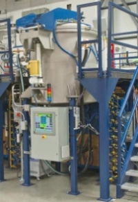
Click to EnlargeMay 24, 2011 – BUSINESS WIRE — GT Solar International Inc. (NASDAQ:SOLR), polysilicon production and sapphire and silicon crystalline growth systems and materials provider, introduced the ASF100 advanced sapphire growth system, which produces larger 100kg sapphire boules in the standard furnace chamber. Larger sapphire substrates enable larger wafers for LED production, increasing throughput and reducing costs via scaling.
With GT Solar’s acquisition of Crystal Systems in 2010, the company made a decision to break into large substrates for the LED market.

Early adopter customers are using the ASF sapphire growth systems as they enter the LED sapphire market, said Cheryl Diuguid, VP and GM, GT Solar sapphire equipment and materials group. Since the commercial introduction of the ASF system in the fall of 2010, GT has booked more than $450 million in orders from new entrants and existing sapphire producers.

Many LED suppliers are ramping to volume production, such as the LUXEON A LED from Philips Lumileds, which is fabbed without binning, and with advanced manufacturing controls. Each LUXEON A LED falls within one 3 step MacAdam ellipse space at actual operating conditions. Philips Lumileds’ Iain Black, ConFab presenter, recently noted that LEDs are essentially chips, as they move from emerging research technology to high-volume wafer processing technologies.

Excelitas Technologies this week opened an LED Center of Excellence at its facility in Shenzhen, PR of China, a center of high-volume manufacturing. The new site will serve as a base for Excelitas Technologies to develop and manufacture advanced LED-based lighting.

The GT Solar ASF sapphire growth systems are designed to be scalable for fast ramps to volume production. The ASF100 provides a highly automated, low risk operating environment, capable of producing consistently uniform sapphire boules for high-brightness LED (HB LED) applications.

GT Solar International, Inc. is a global provider of polysilicon production technology, and sapphire and silicon crystalline growth systems and materials for the solar, LED and other specialty markets. For additional information about GT Solar, please visit www.gtsolar.com.

Subscribe to Solid State Technology/Advanced Packaging.

Follow Solid State Technology on Twitter.com via editors Pete Singer, twitter.com/PetesTweetsPW and Debra Vogler, twitter.com/dvogler_PV_semi.

Or join our Facebook group

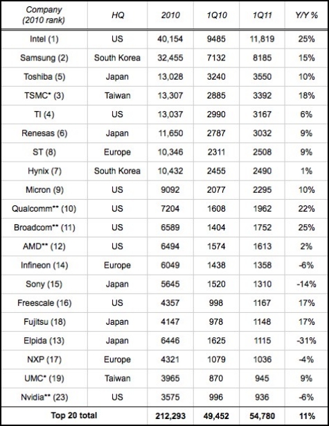
May 23, 2011 – The top 20 semiconductor firms paced at 11% growth in 1Q11, raking in $54.8B in sales, led by the usual suspects, according to rankings from IC Insights.

The top 10 in sales stayed the same, with a couple companies swapping spots: Toshiba leapfrogged into 3rd place ahead of TSMC and TI, while ST and Hynix swapped places (7-8). Intel actually widened its overall lead over Samsung, nearly doubling its rival’s sales growth over the quarter.

Further down the list, DRAM-dependent Elpida was a noticeable slider, from 13 down to 17, with a -31% Y/Y decline by far worst on the list. The other big memory firms (Samsung, Toshiba, Hynix, Micron) all managed at least some growth in the quarter, of which all but Hynix offset DRAM weakness with strong flash memory results. Recall a year ago, memory firms ruled the roost, in part due to a strong rebound, and partly that they suffered less than other sectors.

Also note the ascendance of Nvidia as the fourth "fabless" company in the top 20 list, joining Qualcomm, Broadcom, and now-fabless AMD. Its sales actually shrunk (-6%), but Panasonic’s sales declined by more (-9%). If we were to exclude the two pure-play foundries (perennials TSMC and UMC), Marvell and ON Semi would have been included in these top 20 rankings. (And the combined On Semi-Sanyo Semiconductor entity would be very close to making the list outright, trailing by only $65M or so, IC Insights notes.)

Kudos to top growth, from both sides of the aisle: IDM giant Intel and fabless Broadcom both posted 25% growth in 1Q11, trailed by the other big fabless firm Qualcomm (22%), and foundry ace TSMC (18%). Only seven of the top 20 companies outpaced the group’s 11% average growth, while five suffered losses (NXP, Infineon, Nvidia, Sony, Elpida).

Click to Enlarge
1Q11 top semiconductor sales leaders in US $M.
*Foundry **Fabless (Source: IC Insights, company reports)


May 23, 2011 – Marketwire — Cascade Microtech Inc. (NASDAQ:CSCD), IC measurement product provider, released WinCalXE version 4.5 calibration software, with improved model and process quality. The new version "provides advanced calibration capabilities for the full line of Cascade Microtech probe solutions," said Michael Burger, president and CEO.

WinCalXE 4.5 is a single software tool that contains the features of WinCalXE and SussCal, and operates with all manual and semi-automatic Cascade Microtech and former SUSS MicroTec probe stations.

Burger notes that CSCD is in the midst of many integration tasks stemming from its acquisition of SUSS MicroTec Test Division’s systems and accessories in January 2010 for $98 million. The test systems business specializes in wafer-level test solutions for devices under test (DUT).

WinCalXE 4.5 is used with a vector network analyzer to make on-wafer high-frequency measurements. WinCalXE 4.5 S-parameter data is critical to accurate device characterization, says Cascade Micro.

Vector Network Analyzers do not have internal calibration tools specific to on-wafer measurements, and none offer probe station control, automatic calibrations or advanced on-wafer algorithms. WinCalXE 4.5 can accurately calibrate the measurement system and make automated measurements, data collection and data transformation on Vector Network Analyzers for on-wafer measurements, or measurements requiring on-wafer S-parameter measurements at any frequency up to 500GHz.

WinCalXE 4.5 advanced calibration methods include LRRM and a new LRM+ calibration algorithm. Users can get quick and easy data validation and reporting with automatic measurements using powerful sequencing tools. Users have access to an advanced set-up wizard and multimedia tutorials. WinCalXE 4.5 is fully compatible with Cascade Microtech |Z|Probe, ACP probe and Infinity Probe families and can be used with both ISS and CSR calibration substrates. It is compatible with most commercially available Vector Network Analyzers, ProberBench 7 and all versions of Nucleus probe station software.

Customers with WinCalXE 4.2 or greater, or with any version of SussCal, will receive an upgrade to WinCalXE 4.5 free of charge. Contact the local Cascade Microtech sales office for pricing and order information.

Cascade Microtech Inc. (NASDAQ: CSCD) is a worldwide leader in the precise electrical and mechanical measurement and test of integrated circuits (ICs) and other small structures. For technology businesses and scientific institutions that need to evaluate small structures, Cascade Microtech delivers access to electrical data from wafers, ICs, IC packages, circuit boards and modules, MEMS, 3D TSV, LED devices and more. Cascade Microtech’s leading-edge semiconductor production test products include unique probe cards and test sockets that reduce manufacturing costs of high-speed and high-density semiconductor chips. For more information visit www.cascademicrotech.com.

Subscribe to Solid State Technology/Advanced Packaging.

Follow Advanced Packaging on Twitter.com by clicking www.twitter.com/advpackaging. Or join our Facebook group

By Debra Vogler, senior technical editor

May 23, 2011 — SEMI’s been impressed with the ability of the industry to rebound and recover from the impact of the March 11 Japanese earthquake, noted Tom Morrow, EVP, Emerging Markets Group/Chief Marketing Officer, in an interview at ConFab 2011 (May 15-18, Las Vegas, NV). "By and large, the industry is responding," said Morrow.

Listen to Morrow’s talk:

  • Format: mp3
  • Length: 4:13
  • Size: 3.87 MB
  • Date: 05/23/11


Emerging markets — another major ConFab topic — are important for SEMI members, noted Morrow, and last year, the trade organization created a business unit just for these sectors. In particular, the LED industry is booming with long-term growth. "Many of the suppliers who support that industry are semiconductor suppliers as well," explained Morrow. "They see many of the same needs, some of the same processes and need for standards and industry collaboration that the semiconductor industry has developed to a very high degree." This collaboration will be necessary for the LED industry to reduce costs and accelerate the market.

Morrow noted that the trade organization’s standards program has resulted in a very robust 3D IC standards foundation in place for the manufacturing issues that need to be addressed to enable 3D architectures to prosper efficiently and effectively. “If we go into every system becoming a unique requirement, there will be delays to development of that industry,” said Morrow. SEMI has also supported 450mm standards as well as LED standards, which eliminate the kind of expensive differentiation that doesn’t add any value. “We can focus on innovation, which has always been the mechanism for new markets to be developed.”

More from The ConFab:

Subscribe to Solid State Technology/Advanced Packaging.

Follow Solid State Technology on Twitter.com via editors Pete Singer, twitter.com/PetesTweetsPW and Debra Vogler, twitter.com/dvogler_PV_semi.

Or join our Facebook group

May 23, 2011 — The National Institute of Standards and Technology (NIST) George Mason University (GMU) researchers are studying the optimal characteristics of silicon nanowires and dielectric stacks for charge-trapping memory. The resultant charge-trapping memory devices will offer lower power consumption and faster NVM operation, targeting portable computers and cell phones that operate longer between charging sessions.

NIST’s measurement capabilities were used to determine the best way to design charge-trapping memory devices based on nanowires, which must be surrounded by thin dielectric layers that store electrical charge. Software modeling and electrical device characterization led the NIST and GMU team through a range of dielectric structures to optimize device design.

Click to Enlarge
Click to Enlarge
Figures. In this schematic (top) and transmission electron micrograph (TEM image, bottom), a Si nanowire is shown surrounded by a stack of thin dielectric layers. NIST scientists determined the best arrangement for this dielectric stack for the optimal construction of silicon nanowire-based memory devices. Credit: Schematic: Zhu, GMU. TEM: Bonevich, NIST.

20nm-diameter silicon nano wires form a non-volatile memory (NVM) architecture, retaining contents while power is off, much like flash memory devices. Nanowire memory devices hold an additional advantage over flash memory, which is unsuitably slow for local cache memory in the central processor. "Cache memory stores the information a microprocessor is using for the task immediately at hand," says NIST physicist Curt Richter. "It has to operate very quickly, and flash memory just isn’t fast enough."

Qiliang Li, assistant professor of Electrical and Computer Engineering at GMU, expects their findings to create a platform for more experimenters to further investigate the nanowire-based approach to high-performance NVM, leading to real applications of nanowire-based memory.

Results are published in the journal Nanotechnology:
X. Zhu, Q. Li, D. Ioannou, D. Gu, J.E. Bonevich, H. Baumgart, J. Suehle and C.A. Richter. Fabrication, characterization and simulation of high performance Si nanowire-based non-volatile memory cells. Nanotechnology, May 16, 2011, 22 254020 doi: 10.1088/0957-4484/22/25/254020. Access the article here: http://iopscience.iop.org/0957-4484/22/25/254020 
 
The National Institute of Standards and Technology (NIST) is an agency of the U.S. Department of Commerce. Learn more at http://www.nist.gov/index.html

Meredith Courtemanche, digital media editor

May 18, 2011 — Iain Black, VP WW Manufacturing Engineering, Technology & Innovation, Philips Lumileds, presented "LED Market & Technology" in The ConFab’s final session, which focused on emerging semiconductor technologies.

LEDs are fundamentally semiconductors, Black notes. Just like semiconductors, the die is integrated into a package (which is designed to increase illumination), then assembled into an array, and eventually an end device.

LED manufacturing starts with indium gallium nitride (InGaN) epitaxy growth on a sapphire wafer (2" to 6"). The epi step is accomplished using metal organic chemical vapor deposition (MOCVD). The LED industry is highly interested in using silicon in the future as a substrate. Wafer processing (lithography, etc.) forms the LED, then phosphor is applied at the packaging stage. LEDs are tested, much like semiconductors, before array assembly. Phosphors create LED light colors.

Like in chips, different device architectures are used to form LEDs. Black described vertical thin film devices, which are lower cost but with limited options; lateral die; and thin film flip chips on ceramic substrates, which are AC compatible.

Unlike chip manufacturing, the supplier base is fairly small, Black said, with 2 dominant suppliers for MOCVD tools, for example. And processes lack the level of automation seen in the semi chip fab industry. Wafer size transitions are occuring rapidly, and thicknesses also vary. The forefront of LED fab, much like chip fab, is wafer level packaging (WLP), cluster tools for automation, and advanced substrate materials. Black said "LED devices may just be the ultimate analog compound semiconductor products," if issues such as clear device technology path, performance and cost metrics are met. Standards will go a long way toward this.

The argument for LED bulbs over traditional incandescents is fairly clear from a performance standpoint: 50% efficiency over 5%, 25x longer life, 12W energy consumption to 60W bulb. The initial cost is prohibitive, $40 compared to about 50 cents, but cost over 25,000 hours remains $40, while incandescents will ring up to $165.

Consumer/commercial lighting isn’t the only available market, with camera flash, electronics displays (TVs), and automotive lighting showing sizeable market opportunities. LED market penetration (versus traditional light sources) is accelerating, says Black, with significant upside in outdoor illumination through 2015, steady growth in automotive, and ramping usage for displays and flash. LEDs are a large, and growing, market. Not surprisingly, Taiwan, China, Japan, and Korea dominate LED production by capacity. Vertical integration of LED & Lighting businesses may be a critical success factor here (Philips, Osram, Samsung, LGI, Sharp).

See a summary of Black’s Session 5 co-presenter, David Icke, MC10 Inc., on flexible silicon nano-ribbons here. 

More from the ConFab:


by James Montgomery, news editor

May 18, 2011 –  Bill McClean offered his by-now-familiar overview of electronics and semiconductor market trends. At this point he’s projecting 10% growth in semiconductors to $346.8B, 19% growth in capital spending to $61.7B, and a 9% increase in the materials sales to $47.7B. Updating his famous IC Industry Cycle wheel (think a Chinese New Years calendar for ICs), we’re right in the middle of the best of times with a trio of bullish growth trends (firming prices, a strong market, and aggressive capital spending). The bad news: coming up next are significant capacity additions, then softening prices, and a weak market, a trend that historically takes 3-4 years to work through.

Total worldwide GDP growth will slow a bit to 3.6% in 2011 (vs. 4.3% in 2010). It was originally expected to be 3.9%, but in Japan — which accounts for $174B in electronic components and devices — its prequake 1.5% GDP projetions have been revised down to -2%. Within that overall GDP total, though, emerging markets are surging (6.4%), notably China (9.2%) and India (8.1%) — in fact China’s growth is nearly equaled by its share of total global economics ($4.71T of worldwide $59.22T, or 8.2%).

And as goes worldwide GDP so goes semiconductor industry growth (both ups and downs), particularly tracking together since 2009’s meltdown (global recessions typically are followed by multiple good years) and looking ahead all the way to 2015, McClean showed.

McClean’s forecasts across the board show generally good growth annually through 2015 (high single-digits for electronic systems sales, low-teens for semiconductors, mid/high-teens for capex), all wrapped around a blip in 2013 (2% electronics, -3% semis, -16% capex).

Updating his short-term forecasts for the post-quake world, McClean sees improving climates for electronic system sales (2Q weak, 3Q moderate, 4Q strong) and Japanese GDP ("strongly negative" to "moderately negative" to "moderately positive"), with semiconductor sales activity improving from 2Q’s "moderate" sentiment to "strong" in 3Q, and pulling back to "moderate" in 4Q. Brisk business in 1Q set the table for a solid 2011 — almost without fail since 1984, any 1Q11 growth from the immediately preceding 4Q period has led to double-digit growth for the entire year, he noted. (Speaking of quake impacts, Japan’s the poster child, along with Taiwan, for regions possessing significant seismic risk to IC industry capacity, McClean noted — and the fact that 90% of pure-play foundry capacity is in a seismically active zone should give pause.)

Semiconductor content in electronic devices is still increasing: 25.4% in 2010, up slightly through 2014 to 26.8%, then a notable jump to 28.5% in 2015. PC shipments continue to rise, albeit more slowly in 2011 (12% vs. 18%), but still better than 2009 or 2008 and about the same rate as 2006 and 2007. Cell phone shipment growth will slip in 2011 as well, he said, to 9% from 13%. IC unit volumes are for now right on a 10% long-term trend line, but should move higher in 2H11.

Capital spending should stay at or slightly above/below 16% of sales for the next four years, McClean says; it was ~20% in the early/mid 2000s, and 26% in the late 90s into the 2001-2002 downturn. He sees capital spending rising 19% in 2011 to $61.7B, after more than doubling (101%) in 2010 to $51.8B. The spending continues to narrow to a concentrated few (the top five capex spenders making up 58% of all spending, top 10 is 73%, top 15 is 81%), with even more concentration in 300mm capacity (top 10 = 85%), as exemplified by a power ranking" system meant to illustrate who are likely to be the primary players in future chipmaking capacity additions. (Those not expected to whimper, not flex: fab-lite firms and financially-strapped tier 2 memory suppliers.) The herd will thin even more once the 450mm wafer-size transition comes, McClean asserted, projecting 12 possible 450mm adopters: Intel, Samsung, Toshiba, TSMC as the first, followed by GlobalFoundries and other memory firms, and possibly also by IBM, SMIC, and UMC.