Category Archives: LEDs

April 7, 2011 – BUSINESS WIRE — Tessera Technologies Inc. (Nasdaq:TSRA – News) began two corporate initiatives to enhance the strategic positioning and value of its operations for its stockholders, customers and employees.

Tessera announced today the formation of a new group charged with developing, acquiring and monetizing semiconductor technologies beyond packaging, to be led by Simon McElrea. The group, which will be responsible for an initial portfolio of approximately 280 patents and patent applications, will consist of approximately 40 current employees located in San Jose. Their focus will be on circuitry design, memory modules, 3D architecture, and advanced interconnect technologies, among other areas.

Tessera also announced that it is exploring a possible separation of its Imaging & Optics business. As part of this initiative, Tessera has retained GCA Savvian Advisors, LLC as its financial advisor to assist in the evaluation of multiple alternatives, including, among others, a spin-off transaction.

"Our Imaging & Optics business has had a successful start. We believe under the leadership of its new president, Bob Roohparvar, it may grow more quickly and better serve its customers as a stand-alone entity, and we have begun the work of exploring alternative means to that end," added Nothhaft.

Tessera has not set a definitive timetable for completing its exploration of alternatives for the Imaging & Optics business and there can be no assurance that the process will result in any transaction. The company does not expect to make further public comment regarding these matters unless a definitive agreement or other commitment for any transaction is reached.

Tessera Technologies, Inc., develops, invests in, licenses and delivers innovative miniaturization technologies and products for next-generation electronic devices. Go to www.tessera.com.

Subscribe to Solid State Technology/Advanced Packaging.

Follow Advanced Packaging on Twitter.com by clicking www.twitter.com/advpackaging. Or join our Facebook group

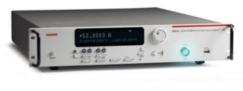
April 6, 2011 — Keithley Instruments Inc., advanced electrical test instruments and systems provider, introduced the Model 2651A High Power System SourceMeter instrument to characterize high-power electronics.

Click to EnlargeThe Model 2651A claims the widest current range available in the industry, suiting R&D, reliability, and production test applications, such as testing high-brightness LEDs (HB-LEDs), power semiconductors, DC-DC converters, batteries, and other high-power materials, components, modules, and subassemblies.

Like each member of the Series 2600A family, the Model 2651A offers a highly flexible, four-quadrant voltage and current source/load coupled with precision voltage and current meters. It combines the functionality of multiple instruments in a single full-rack enclosure: semiconductor characterization instrument, precision power supply, true current source, DMM, arbitrary waveform generator, V or I pulse generator, electronic load, and trigger controller, and is fully expandable into a multi-channel, tightly synchronized system via Keithley’s TSP-Link technology. The Model 2651A can source or sink up to 2,000W of pulsed power (±40V, ±50A) or 200W of DC power (±10V@±20A, ±20V@±10A, ±40V@±5A). It can also make precise measurements of signals as low as 1pA and 100 microvolts at speeds up to one microsecond per reading.

The user can chose digitizing or integrating measurement modes for precise characterization of both transient and steady-state behavior. Two independent analog-to-digital (A/D) converters define each mode — one for current and the other for voltage — which run simultaneously for accurate source readback.

The digitizing measurement mode’s 18-bit A/D converters allow capturing up to one million readings per second for continuous one-microsecond-per-point sampling, making this mode the most appropriate choice for waveform capture and measuring transient characteristics with high precision. Competing solutions must average multiple readings to produce a measurement result and often don’t allow the measurement of transient behavior.

The integrating measurement mode, based on 22-bit A/D converters, optimizes the instrument’s operation for applications that demand the highest possible measurement accuracy and resolution. This ensures precise measurements of the very low currents and voltages common in next-generation devices. All Series 2600A instruments provide integrating measurement mode operation.

Connecting two Model 2651A units in parallel via TSP-Link expands the system’s current range from 50A to 100A. This is 2.5-5x greater than the nearest competing solution. The voltage range can be expanded from 40 to 80V when two units are connected in series. The embedded Test Script Processor (TSP) included in all Series 2600A instruments simplifies testing by allowing users to address multiple units as a single instrument so that they act in concert. The built-in trigger controller in the Model 2651A can synchronize the operation of all linked channels to within 500 nanoseconds. These capabilities of the Model 2651A provide the broadest dynamic range available in the industry, making the unit suitable for a broad variety of high current, high power test applications, including:

  • Power semiconductor, HBLED, and optical device characterization and testing
  • Characterization of GaN, SiC, and other compound materials and devices
  • Semiconductor junction temperature characterization
  • Reliability testing
  • High speed, high precision digitization
  • Electromigration studies

To minimize device self-heating during tests, a common problem with high-power semiconductors and materials, the Model 2651A offers high-speed pulsing capabilities that allow users to source and measure pulses with high accuracy. Pulse widths from 100 microseconds to DC and duty cycles from 1 to 100% are programmable. Competing solutions are typically hampered by limited flexibility for programming the instrumentation’s duty cycle.

TSP Express, Keithley’s LXI-based I-V test software utility, is embedded in the instrument. From basic to advanced tests, TSP Express delivers device data in three easy steps: connect, configure, and collect. It also simplifies connecting instruments to allow higher pulsing levels. Results can be viewed in either graphical or tabular format and then exported to a .csv file for use with spreadsheet applications. Two other powerful software tools for creating test sequences are also provided. The Test Script Builder application supports creating, modifying, debugging, running, and managing TSP scripts. An IVI-based LabVIEW driver simplifies integrating the Model 2651A into LabVIEW test sequences.

To learn more, visit the Model 2651A product page: http://www.keithley.com/products/dcac/currentvoltage/highcurrent/?mn=2651A

Subscribe to Solid State Technology/Advanced Packaging.

Follow Advanced Packaging on Twitter.com by clicking www.twitter.com/advpackaging. Or join our Facebook group
April 6, 2011LED technology adoption for LCD backlight applications and general lighting purposes fuels ever-growing demand, and LED manufacturers are poised to meet it, according to the newest update of the SEMI Opto/LED Fab Forecast. The industry has attracted a huge amount of capital pouring into the LED supply chain from equipment and materials to LED epitaxy/chip fabrication and LED packaging capacity.

The SEMI Opto/LED Fab Forecast tracks over 250 Opto/LED fabs activities worldwide, with detailed information on fab construction and equipment spending, key milestone dates, capacity and ramp up schedule, and more.

Last year, SEMI recorded explosive growth on equipment spending from LED fabs, jumping from $606 million in 2009 to $1.78 billion in 2010. SEMI expects that LED equipment growth will continue this year to reach about $2.5 billion, a 40% increase year-over-year. If some projects do not ramp up as quickly as planned, then some spending will be pushed to 2012. Currently, SEMI forecasts the 2012 investment level as $2.3 billion worldwide.

Regional equipment spending shows an aggressive investment trend from China. Propped up by subsidy programs from local governments in China, new LED fab projects have blossomed in the past two years in China.  China now accounts for almost 50% of overall equipment spending.    

Recent LED fab investments:

In regards to new LED fabs, SEMI recorded 19 new fabs that started operation in 2010, with another 27 new operation fabs expected in 2011. For 2012, SEMI forecasts 15 new fabs coming online next year.  
 
On the capacity side, according to the SEMI Opto/LED Fab Forecast, worldwide LED fab capacity reached 4,350 thousand wafers per month (wpm, 2" wafer equivalent). SEMI expects strong demand from LCD backlight to continue to drive the capacity growth in 2011 with a 50% increase to reach 6,509 thousand wpm (2" equiv.).  

The SEMI Opto/LED Fab Forecast can be found at http://www.semi.org/en/Store/MarketInformation/OptoLEDFabForecast

SEMI is the global industry association serving the manufacturing supply chains for the microelectronic, display and photovoltaic industries. For more information, visit www.semi.org

Also read: LCD, OLED manufacturing equipment on a growth tear

Subscribe to Solid State Technology/Advanced Packaging.

Follow Solid State Technology on Twitter.com via editors Pete Singer, twitter.com/PetesTweetsPW and Debra Vogler, twitter.com/dvogler_PV_semi.

Or join our Facebook group

April 5, 2011 — With the first observation of thermoelectric effects at graphene contacts, University of Illinois researchers found that graphene transistors have a nanoscale cooling effect that reduces their temperature.
 
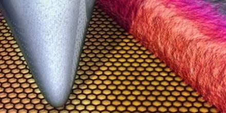
The Illinois team used an atomic force microscope (AFM) tip as a temperature probe to make the first nanometer-scale temperature measurements of a working graphene transistor. The measurements revealed surprising temperature phenomena at the points where the graphene transistor touches the metal connections. They found that thermoelectric cooling effects can be stronger at graphene contacts than resistive heating, lowering the temperature of the transistor.

Click to Enlarge

Image: An atomic force microscope tip scans the surface of a graphene-metal contact to measure temperature with spatial resolution of about 10nm and temperature resolution of about 250 mK.  Color represents temperature data. Alex Jerez, Beckman Institute Imaging Technology Group.

Future computer chips made out of graphene could be faster than silicon chips and operate at lower power, if scientists can grasp a thorough understanding of heat generation and distribution in graphene devices.

The researchers were led by mechanical science and engineering professor William King and electrical and computer engineering professor Eric Pop.

All electronics dissipate heat as a result of the electrons in the current colliding with the device material, a phenomenon called resistive heating. This heating outweighs other smaller thermoelectric effects that can locally cool a device. The speed and size of computer chips are limited by how much heat they dissipate. Computers with silicon chips use fans or flowing water to cool the transistors, a process that consumes much of the energy required to power a device. Graphene’s apparent self-cooling effect means that graphene-based electronics could require little or no cooling.

"In silicon and most materials, the electronic heating is much larger than the self-cooling," King said. "However, we found that in these graphene transistors, there are regions where the thermoelectric cooling can be larger than the resistive heating, which allows these devices to cool themselves. This self-cooling has not previously been seen for graphene devices."

"Our measurements and simulations project that thermoelectric effects will become enhanced as graphene transistor technology and contacts improve," said Pop, who is also affiliated with the Beckman Institute for Advanced Science, and the Micro and Nanotechnology Laboratory at the U. of I.

Next, the researchers plan to use the AFM temperature probe to study heating and cooling in carbon nanotubes (CNTs) and other nanomaterials.

King also is affiliated with the department of materials science and engineering, the Frederick Seitz Materials Research Laboratory, the Beckman Institute, and the Micro and Nanotechnology Laboratory.

The Air Force Office of Scientific Research and the Office of Naval Research supported this work.

The team published its findings in the April 3 online edition of the journal Nature Nanotechnology (http://www.nature.com/nnano/journal/vaop/ncurrent/full/nnano.2011.39.html). Co-authors of the paper included graduate student Kyle Grosse, undergraduate Feifei Lian and postdoctoral researcher Myung-Ho Bae.

Follow Small Times on Twitter.com by clicking www.twitter.com/smalltimes. Or join our Facebook group

April 4, 2011 — Nanoco Group plc (AIM: NANO), cadmium-free quantum dots  manufacturer, produced a 1kg batch of red cadmium-free quantum dots (CFQD) for a major Japanese corporation, which triggers a US$2 million payment to Nanoco by the corporation.

The production of cadmium-free quantum dots on this scale is a major technical achievement that required scalability in Nanoco’s patent-protected technology and the expertise of its production and technical teams.

The 1kg of red CFQD was manufactured to specification at Nanoco’s recently commissioned production facility in Runcorn, Cheshire, UK.

Nanoco expects to be able to demonstrate that green CFQD meet technical milestones within the next few months, which will trigger a milestone payment of US$1 million. This will be followed by the production of 1kg of green CFQD for delivery to the same customer in the second half of 2011. Once validated, the green CFQD will also attract a US$2 million milestone payment.

Also read: Making quantum dots less toxic broadens users’ options 

Nanoco develops and manufactures commercial quantities of quantum dots for use in multiple applications including lighting, solar cells, and biological imaging. Nanoco’s quantum dots, which are free of heavy metals and comply with RoHS legislation, can be combined into a wide range of materials including liquids, polymers and glass. Nanoco forms strategic partnerships with major end users across a range of applications. Nanoco began trading on the AIM market of the London Stock Exchange in May 2009 under the ticker symbol NANO. Learn more at http://www.nanocotechnologies.com/.

Follow Small Times on Twitter.com by clicking www.twitter.com/smalltimes. Or join our Facebook group

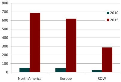
April 1, 2011 Solid state non-volatile memory (NVM) chips, which retain data when the power is off, are expected to see phenomenal growth in the next five years. According to a recently published report from iRAP Inc., ET-114: Advanced Solid-State Memory Systems and Products: Emerging Non-volatile Memory Technologies, Industry Trends and Market Analysis, the global market for emerging non-volatile random access memory products was projected to have reached $115 million in 2010.

This market is expected to increase to $1.6 billion by 2015 at an average annual growth rate (AAGR) of 69% through the forecast period.

Click to Enlarge
Figure. Market share for emerging advanced solid state non-volatile random access memory products by region, 2010 and 2015. ($ Millions) Source: iRAP, Inc. April 2011.

Regionally, North America captured about 42% of the market in 2010, followed by Europe at 36%, and the rest of the world (ROW) with 22%, dominated by Japan, Korea and China.

Combining medium-speed random access memory for continuously changing data, a high-speed memory for caching instructions to the CPU, and a slower, non-volatile memory for long-term information storage when the power is removed into a single memory has been a long-standing goal of the semiconductor industry

Seven emerging non-volatile memory technologies such as FERAM, phase change random access memory (PCM, PC-RAM, PRAM, OUM), magneto-resistive RAM (MRAM, STT RAM, Race Track Memory), resistance switching RAM (RRAM, ReRAM, CB-RAM, PMC-RAM, Nanobridge RAM CMOx, memistors), zero capacitor (ZRAM), quantum dot RAM and polymer printed memory are contributing to this growth.

The market for emerging non-volatile random access memory used as an embedded system on chip (SOC) cards in 2010 was the highest. This is followed by RFID tags used in goods, which are transported by high-speed detection conveyors, as in airports and smart airbags used in automobiles. The remaining four market applications are radiation-hardened memory in aerospace and nuclear installations, printed memory platforms such as smart cards, games, sensors, display, storage-class memory network and high end smart mobile phones.

Among the seven emerging non-volatile random access memory technologies covered in this report, in 2010 the potential market for zero capacitor (ZRAM) was highest. The polymer printed memory market in 2010 was next highest, followed by ferromagnetic RAM as a distant third.

In 2015, phase change memory (PCM, PC-RAM, PRAM, OUM) will be highest. FeRAM will be next highest, followed by zero capacitor RAM (ZRAM).

MRAM promises a high capacity, next-generation memory that can replace SRAM/flash combos and battery-backed up RAM as well as supplying improved non-volatile memory solutions for high-end mobile products. MRAM is already in the sampling stage. Freescale has just recently moved MRAM into volume production, and there are as many as 20 firms actively pursuing this opportunity. Meanwhile, important firms such as Intel, Freescale, Micron, Samsung, STMicroelectronics are beginning to settle on new technology platforms for the post-flash era and are finding ovonic and nano-crystalline memories increasingly satisfactory.

Region 2010 ($ Mil.) % 2015 ($ Mil.) % AAGR- 2010-15
North America 48.3 42 684 43 69.8
Europe 46.0 40 620 39 68.2
ROW 20.7 18 286 22 69
Total 115 100 1590 100 69

Table. Global market for emerging advanced solid state non-volatile random access memory products by region through 2015. ($ Millions) Source: iRAP, Inc.

More details of the report are available from Innovative Research and Products (iRAP), Inc., P.O. Box 16760, Stamford, CT 06905. Visit http://www.innoresearch.net/reportlist.aspx?cid=4 or contact iRAP at 203-569-7909; [email protected]

Subscribe to Solid State Technology/Advanced Packaging.

Follow Solid State Technology on Twitter.com via editors Pete Singer, twitter.com/PetesTweetsPW and Debra Vogler, twitter.com/dvogler_PV_semi.

Or join our Facebook group

By Debra Vogler, senior technical editor

April 1, 2011 — Daniel Duffy, research scientist in Henkel’s Advanced Technology Group, was a presenter at MEPTEC’s The Heat is On event (3/21/11, Santa Clara, CA). Summarizing the encapsulant materials used for high-brightness LEDs (HB-LEDs), he noted the pros and cons of epoxy and silicone. The material challenges for epoxies are temperature stability and color (aging); and for silicone, contamination and adhesion, as well as barrier properties. In the future, epoxies will have to be stable with respect to blue light (T>150ºC); and silicone material will have to fulfill the condition T<Tg CTE <60ppm/K. "Silicone encapsulants are very stable," said Duffy. "But it is not enough — future power demands require higher levels of photo-thermal stability."

Die attach material challenges include transparency, CTE, interfacial TC, and adhesion properties. Such materials will need to have stable thermal resistance, high TC, matched TCE, and good adhesion properties. Duffy specifically mentioned adhesion as a critical property for LED packaging. "Delamination leads to increased interfacial thermal resistance," said Duffy. "Localized temperature increases can shorten device life." Furthermore, cracking can lead to weakening of wire bonds and cracks; also, delamination weakens barrier protection.

In this podcast interview, Duffy discusses the outlook for new materials and/or enhanced materials for HB-LED applications, including quantum dots. "Quantum dots are very interesting materials…when we learn how to tune the interactions between then and the rest of the materials involved in LED packaging, they will play a continuous role in the future," said Duffy. "They offer a wide variety of colors, tunability of color, and lots of options for tuning their performance with temperature, with time and, maybe even other optical effects we’re not even considering now…they’re here to stay."  The challenge, he noted, will be getting them into materials for higher-power applications.

Listen to Duffy’s podcast interview:  Download (iPhone/iPod users) or Play Now


Subscribe to Solid State Technology/Advanced Packaging.

Follow Advanced Packaging on Twitter.com by clicking www.twitter.com/advpackaging. Or join our Facebook group

April 1, 2011 – Marketwire — With escalating demand for larger fabs of Gen 8, Gen 8.5 and Gen 10, the liquid crystal display (LCD) and organic light emitting diode (OLED) manufacturing equipment market has witnessed a growth spur. The market will continue its upward growth trajectory through 2011, says analyst firm Frost & Sullivan.

The majority of demand stems from the Gen 8 and Gen 8.5 segment. Burgeoning sales of LCD TVs, smartphones, and advertising screens is triggering high uptake of LCD manufacturing equipment.

During 2010, TFT-CD fab expansions boosted LCD equipment adoption. The intensifying focus on energy efficiency and the gravitation toward environment-friendly products will accelerate demand for OLED displays over the next 3-5 years.

New analysis from Frost & Sullivan, LCD and OLED Manufacturing Equipment Market, finds that the market earned revenues of $7300.3 million and $136.7 million respectively in 2009 and estimates this to reach $18,182.5 million and $702.7 million in 2017.

"The tangible advantages of OLED technology, such as sharper images and better contrast ratios, crisp colors and faster refresh rates compared to any existing display technology will be a key driver," says Frost & Sullivan research analyst Lavanya Rammohan. "OLED also offers consumers better energy management, as the whole system functions at optimal power and is of organic substrate."

As the benefits of OLED displays become more prominent, the demand for OLED manufacturing equipment will witness a hike in the next 3-7 years. Technology innovations, better functionality, and falling prices are expected to keep up the tempo of demand for OLED displays in mobile phones. The market also expects to benefit from increasing demand for OLED displays used for signage.

Deposition and patterning of large substrates remain major impediments for LCD and OLED manufacturing equipment providers. The use of large substrates complicates the deposition process and incurs high capital costs in terms of material deposition and relevant technical issues with throughput and uniform deposition.

Greater emphasis on design and prototyping will continue to revolutionize the display manufacturing equipment markets. As the consumer industry continues to witness increasing panel sizes, deposition with high accuracy and throughput (without affecting integrity of material in the OLED market) will be a key challenge.

"LCD and OLED equipment manufacturers are constantly improving design and functionality of equipment to help overcome deposition challenges and battle bottlenecks," says Rammohan. "They are venturing into open collaboration with customers and creating product roadmaps that enable scalability for future generations of display manufacturing."

Innovative deposition techniques, testing and other processes are expected to spike customer interest and elevate purchasing levels. Going forward, there will be increased collaboration between material providers, display manufacturers, equipment providers and technology enablers to optimize material performance and lifetime. Constant manufacturing process improvement will be imperative to balance the relentless price pressures that confront display manufacturers.

LCD and OLED Manufacturing Equipment Market is part of the Surface Mount Technologies Growth Partnership Service program. All research services included in subscriptions provide detailed market opportunities and industry trends that have been evaluated following extensive interviews with market participants.

If you are interested in a virtual brochure for this study, e-mail Sarah Saatzer, Corporate Communications, at [email protected], with your full name, company name, job title, telephone number, company e-mail address, company website, city, state and country, or visit http://www.frost.com.

Subscribe to Solid State Technology/Advanced Packaging.

Follow Solid State Technology on Twitter.com via editors Pete Singer, twitter.com/PetesTweetsPW and Debra Vogler, twitter.com/dvogler_PV_semi.

Or join our Facebook group

March 31, 2011 — Researchers from North Carolina State University have investigated the viability of a technique called spincasting for creating thin films of nanoparticles on an underlying substrate, creating materials with a variety of uses, from optics to electronics.

Spincasting, which utilizes centrifugal force to distribute a liquid onto a solid substrate, already has a variety of uses. For example, it is used in the electronics industry to deposit organic thin films on silicon wafers to create transistors.

Click to Enlarge

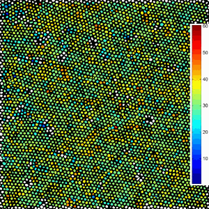
Figure. This is an orientation map of a spin-cast array of FePt nanoparticles. Most nanoparticles are enclosed by a hexagon of six neighboring nanoparticles. Each nanoparticle was color coded according to the angle (in degrees) of the hexagon’s orientation.

For this study, the researchers first dispersed magnetic nanoparticles coated with ligands into a solution. The ligands, small organic molecules that bond directly to metals, facilitate the even distribution of the nanoparticles in the solution and, later, on the substrate itself.

A drop of the solution was then placed on a silicon chip that had been coated with a layer of silicon nitride. The chip was then rotated at high speed, which spread the nanoparticle solution over the surface of the chip. As the solution dried, a thin layer of nanoparticles was left on the surface of the substrate.

Using this technique, the researchers were able to create an ordered layer of nanoparticles on the substrate, over an area covering a few square microns.

Dr. Joe Tracy, an assistant professor of materials science and engineering at NC State and co-author of a paper describing the study, explained that one benefit of spincasting is that it is a relatively quick way to deposit a layer of nanoparticles. "It also has commercial potential as a cost-effective way of creating nanoparticle thin films," Tracy says.

However, the approach still faces several hurdles. Tracy notes that modifications to the technique are needed, so that it can be used to coat a larger surface area with nanoparticles. Additional research is also needed to learn how, or whether, the technique can be modified to achieve a more even distribution of nanoparticles over that surface area.

Analysis of the nanoparticle films created using spincasting led to another development. The researchers adapted analytical tools to evaluate transmission electron microscopy (TEM) images of the films they created. One benefit of using these graphical tools is their ability to identify and highlight defects in the crystalline structure of the layer. "These methods for image analysis allow us to gain a detailed understanding of how the nanoparticle size and shape distributions affect packing into monolayers," Tracy says.

The paper, "Formation and Grain Analysis of Spin Cast Magnetic Nanoparticle Monolayers," was published online March 24 by the journal Langmuir. The paper was co-authored by Tracy; NC State Ph.D. student Aaron Johnston-Peck; and former NC State post-doctoral research associate Dr. Junwei Wang. The research was funded by the National Science Foundation, the U.S. Department of Education, and Protochips, Inc.

Abstract: Ligand-stabilized magnetic nanoparticles (NPs) with diameters of 4-7 nm were spin cast into monolayers on electron-transparent silicon nitride (SiN) substrates. SiN membranes facilitate detailed high-resolution characterization of the spin-cast monolayers by transmission electron microscopy (TEM) and approximate spin casting onto wafers. Suspending the NPs in hexanes and pretreating the substrate with ultraviolet light and ozone (UVO) gives the best results. Computer-aided analysis of the arrays elucidates their grain structures, including identification of the grain boundaries and defects and measurements of the grain orientations and translational correlation lengths. Narrow NP size distributions result in close-packed arrays with minimal defects and large grains containing thousands of NPs. Edge dislocations, interstitials, vacancies, and overlapping NPs were observed. Deviations from close packing occur as the normalized standard deviation of the sample’s size distribution increases above approximately 11%. Polydisperse size distributions and deviations from spherical NP shapes frustrate assembly and prevent ordered packing.
Access: http://pubs.acs.org/doi/abs/10.1021/la200005q

NC State’s Department of Materials Science and Engineering is part of the university’s College of Engineering.