Category Archives: LEDs

March 30, 2011 – BUSINESS WIREaustriamicrosystems (SIX:AMS) conditionally released its advanced 0.18µm High-Voltage CMOS process technology "H18" to for volume production. It will be manufactured in IBM’s 200mm Burlington, VT, wafer facility.

Jointly developed with IBM, the 0.18µm High-Voltage CMOS process is the 6th generation of continuously improved High-Voltage CMOS technologies developed at austriamicrosystems.

Featuring a new level of RF and HV integration capability on a single IC, the new 0.18µm High-Voltage CMOS process offers integration density up to 118k gates/mm2, enabling system on chip (SoC) applications and power-on resistance (Rdson) for silicon area reduction. The integration capabilities of H18 enable design houses and IDMs to create new applications in areas such as smart sensors, sensor interface devices, smart meters, industrial and building controls and LED lighting control.

Only a few mask level adders are required on top of the fully compatible CMOS base process to implement high-voltage capabilities. The process allows the integration of 1.8V, 5V, 20V and 50V devices on a single chip without process modifications. Process features such as Schottky barrier diode, high-resistive and precision poly, single- and dual metal-insulator-metal (MIM) capacitors, varactors and up to 7 metal layers including thick last metal complete the High-Voltage H18 CMOS process.

Modular SoC designs using H18 can integrate analog high-voltage blocks with RF CMOS, extended digital functions and micro-controllers, said Thomas Riener, SVP and GM of austriamicrosystems’ Full Service Foundry business unit. "The H18 technology is now ramping in a broad range of smart green applications such as power management for photovoltaics and LED driver applications."

Learn more at http://www.austriamicrosystems.com 

Subscribe to Solid State Technology/Advanced Packaging.

Follow Solid State Technology on Twitter.com via editors Pete Singer, twitter.com/PetesTweetsPW and Debra Vogler, twitter.com/dvogler_PV_semi.

Or join our Facebook group

John Robinson, director of marketing, Process Control Information Division (PCID), KLA-Tencor (KLAC)

March 30, 2011 — In-line automated inspection during wafer fabrication allows high defect capture rates (consistency, accuracy) and rapid classification (time-to-results) of mission-critical defects. However, to achieve the most value from a comprehensive automated inspection investment, advanced defect analysis is needed. Incorporating defect data from multiple inspections throughout the LED manufacturing process into one environment provides a holistic approach, as well as unprecedented process control and yield improvement.

Many LED fabs currently have only basic manual methods to perform defect and yield analysis. The bulk of engineering time is spent gathering and formatting, slowing time to results. Too often, methods are inconsistent, without advanced analysis tools, and lack connectivity between process areas, such as incoming bare wafer inspection, epi inspection, patterned wafer inspection, post dice inspection, and final electrical yield probe inspection.

A better approach includes a centralized database capable of handling inspection data and images, metrology data, yield bin data, as well as fab process inputs. Combined with advanced analysis tools and automation, engineers can quickly and effectively get results.

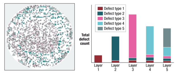
Click to Enlarge

Figure. Advanced defect source analysis (DSA). KLARITY LED provides defect source analysis including interactive wafer maps and images.

Defect source analysis (DSA) (see figure) includes both qualitative and quantitative methods to determine where in the process defects are introduced, which defects are common from one process step to the next, and how the defects propagate throughout the production line. Knowing, for example, that defects found post-dice originated back in the epi process will save valuable time identifying the root cause and will reduce the amount of material at risk.

Spatial signature analysis (SSA) enables automated detection of defect signatures, such as scratches or other characteristic spatial patterns. Frequently, simple statistical process control (SPC) on overall defect counts is insufficient to detect problems with unique assignable causes that can readily be identified with SSA. For example, an intermittent resist spin-on issue may appear to be a random scratch. Identified by SSA and viewed as an aggregate over many wafers, however, the tell-tale wagon-wheel pattern can be readily identified.

The LED industry is beginning to adopt stepper-based projection lithography. This introduces an additional class of defects, called repeating defects to distinguish them from random defects. Defects introduced as part of stepper-based lithography can repeat from projection field to projection field many times across an individual wafer, as well as from wafer to wafer. Repeater defect analysis tools can quickly determine if the lithographic process is drifting out of spec and save many die that would otherwise fail as non-yielding die.

A defect early in the manufacturing process wastes not only the costs related to the defective wafer itself, but also any additional processing of the defective wafer, and the costs of any additional wafers that suffer yield loss before the excursion is identified. By inserting in-line inspection points at significant process milestones, as well as adopting advanced defect analysis solutions, manufacturers can catch excursions sooner, reducing the amount of product at risk.

Minor excursions are due to a shift in process parameters that is not significant enough to trigger an alarm using only basic SPC methods. It is difficult to differentiate a minor excursion from normal variations in baseline without higher-sensitivity automated inspection and advanced automated analysis tools. Over a period of time, these minor excursions can add up to significant yield loss. Combining in-line inspection with advanced defect analysis provides the fastest possible excursion detection, root-cause troubleshooting analysis, and yield correlation.

John Robinson is a director of marketing in the Process Control Information Division (PCID) at KLA-Tencor, and is responsible for the Klarity LED product line. With KLA-Tencor for more than 13 years, he has held positions in several metrology and inspection applications groups. He holds a Ph.D. in physics from The University of Texas at Austin. Learn more and contact the company at www.kla-tencor.com

Also read: KLA-Tencor debuts LED substrate/epi wafer inspection system

Subscribe to Solid State Technology/Advanced Packaging.

Follow Solid State Technology on Twitter.com via editors Pete Singer, twitter.com/PetesTweetsPW and Debra Vogler, twitter.com/dvogler_PV_semi.

Or join our Facebook group

March 28, 2011 — Tabula Inc., a privately held fabless semiconductor company and developer of the ABAX family of 3D Programmable Logic Devices (3PLDs), secured $108 million in Series D funding. Tabula will use the new capital to accelerate production of their 3PLD ABAX product family, expand customer and partner support infrastructures, and further next-generation product development in the rapidly growing programmable logic sector.

The financing was led by Crosslink Capital and DAG Ventures. Existing investors, Balderton Capital, Benchmark Capital, Greylock Partners, Integral Capital, and NEA also participated in this round.

"The programmable logic market is seeing tremendous growth driven by the build out of the telecommunications infrastructure. This infrastructure build is necessary to keep pace with the global demand for more bandwidth to support smartphone usage for accessing data and video online," said Dennis Segers, CEO of Tabula. He said the company will increase volume shipments of its ABAX 3PLD product family and use the Spacetime architecture to integrate programmable devices into new application spaces. Tabula’s 3D programmable logic devices are high-capability programmable chips made in production volumes.

"Tabula’s Spacetime technology addresses the problems at the heart of the programmable logic market today by delivering unprecedented capabilities at unmatched cost points compared to FPGAs," said Gary Hromadko, Venture Partner of Crosslink Capital. "Tabula is well positioned to capitalize on the growing migration of ASIC and ASSP towards programmable logic devices," added Dave Strohm, Partner of Greylock Partners.

Tabula recently completed the roll-out of its 40nm ABAX family of 3PLDs supported by the Stylus development software. Stylus delivers Spacetime’s 3D Architecture price/performance advantages to ASIC and FPGA designers, maintaining a familiar design flow. Available in the cloud, Stylus eliminates IT issues while enabling real-time, on-site-like, technical support.

"Tabula has an unbounded $70B market opportunity," said Bruce Dunlevie, General Partner of Benchmark Capital.

Tabula is a privately held fabless semiconductor company developing 3D Programmable Logic Devices. Its ABAX family of 3PLDs, based on Tabula’s patented Spacetime architecture, and supported by its Stylus development software, sets new density, performance, and affordability benchmarks for programmable logic, memory, and signal processing. Please visit www.tabula.com.

Subscribe to Solid State Technology/Advanced Packaging.

Follow Solid State Technology on Twitter.com via editors Pete Singer, twitter.com/PetesTweetsPW and Debra Vogler, twitter.com/dvogler_PV_semi.

Or join our Facebook group

March 28, 2011 — Studies done by Mark Lusk and colleagues at the Colorado School of Mines could significantly improve the efficiency of solar cells. Their latest work describes how the size of light-absorbing particles — quantum dots — affects the particles’ ability to transfer energy to electrons to generate electricity.

They provide evidence to support a controversial idea, called multiple-exciton generation (MEG), which theorizes that it is possible for an electron that has absorbed light energy, called an exciton, to transfer that energy to more than one electron, resulting in more electricity from the same amount of absorbed light.

The results are published in the April issue of the journal ACS Nano.
 
The idea of quantum dots improving solar cells is not new, as Katherine Derbyshire reported in 2007, but it has yet to be commercialized. For this study, Lusk and collaborators used a National Science Foundation (NSF) supported high-performance computer cluster to quantify the relationship between the rate of MEG and quantum dot size.
 
They found that each dot has a slice of the solar spectrum for which it is best suited to perform MEG and that smaller dots carry out MEG for their slice more efficiently than larger dots. This implies that solar cells made of quantum dots specifically tuned to the solar spectrum would be much more efficient than solar cells made of material that is not fabricated with quantum dots.
 
According to Lusk, "We can now design nanostructured materials that generate more than one exciton from a single photon of light, putting to good use a large portion of the energy that would otherwise just heat up a solar cell."
 
Quantum dots are man-made atoms that confine electrons to a small space. They have atomic-like behavior that results in unusual electronic properties on a nanoscale. These unique properties may be particularly valuable in tailoring the way light interacts with matter.
 
Experimental verification of the link between MEG and quantum dot size is a hot topic due to a large degree of variation in previously published studies. The ability to generate an electrical current following MEG is now receiving a great deal of attention because this will be a necessary component of any commercial realization of MEG.

The research team, which includes participation from the National Renewable Energy Laboratory (NREL), is part of the NSF-funded Renewable Energy Materials Research Science and Engineering Center at the Colorado School of Mines in Golden, CO. The center focuses on materials and innovations that will significantly impact renewable energy technologies. Harnessing the unique properties of nanostructured materials to enhance the performance of solar panels is an area of particular interest to the center.
 
"These results are exciting because they go far towards resolving a long-standing debate within the field," said Mary Galvin, a program director for the Division of Materials Research at NSF. "Equally important, they will contribute to establishment of new design techniques that can be used to make more efficient solar cells."

Learn more at http://www.mines.edu/

Subscribe to Photovoltaics World

Follow Photovoltaics World on Twitter.com via editors Pete Singer, twitter.com/PetesTweetsPW and Debra Vogler, twitter.com/dvogler_PV_semi.

Or join our Facebook group

by James Montgomery, news editor

March 25, 2011 – Applied Materials had its Analyst Day on March 23. Key takeaways included: Where wafer-fab equipment demand is strongest, how solar manufacturing technology can expand, and why tablet computers and electric vehicles are underpinning a resurgence in 200mm demand.

Quickly updating on the Japan earthquake & tsunami situation, AMAT chairman/CEO Mike Splinter noted that the company’s 650 staff and families are all safe; some of the company’s 22 facilities in Japan sustained minor damage but all are back in operation, he noted. There has been "minor impact" on customers, but so far there has been "no material impact" on AMAT through 2Q11 — though the situation is still "dynamic and unpredictable," he added. Joe Flanagan, SVP of operations, added that the company has been able to address risks for all its Tier 1 and Tier 2 suppliers, and in some places concluded mitigation plans. There’s some infrastructure questions, but "we’re making prudent assumptions" and planning around them, he said.

Growth in SSG/semiconductors. AMAT EVP Rhandir Thakur offered updates on the semiconductor sector as a whole and the company’s own numbers:

  • Revenue growth of 170% — outpacing the overall WFE sector, thanks to gains in 2009/2010. Operating profit model targets $1.9B (Semitool is turning accretive ahead of plan). 2011 priorities for SSG: launch >12 new products, gain >1% share in 300mm WFE, >$2B profit.
  • AMAT still expects 18 new fabs/expansions in the next 2-3 years, translating to 1.2M more wafer starts/month, and $70B-$80B in WFE spending.
Click to Enlarge
(Source: Gartner, Applied Materials)

The company reiterated its areas of share gain since 2008: six points each in PVD and transistor fabrication, seven in CMP, and two in CVD. Translation: $1.5B growth in revenues. Looking forward AMAT expects four points in etch (foundries and memory), and some inspection; in plating/ECP the addition of Semitool has helped with business in both interconnect and wafer-level packaging.

Thakur noted that moving from the 65nm to 2Xnm node, memory and foundry/logic makers will be adding over 150 process steps. And more than 70% wafer starts in 2012 will be on advanced nodes (≤45nm process technologies), and that’s where 80% of spending goes. Added complexity — including 3D chip technologies, transition to HKMG, and EUV lithography (especially if it’s delayed) — is good news for AMAT, he summed.

Solar steady, LEDs coming up. EVP Mark Pinto pointed to HB-LED, new products for c-Si PV and "product enhancements" for thin-film PV. New growth is seen in extending Baccini Esatto technology in front metal, point contact, and selective emitter, enabling "up to a 2 point efficiency gain," though this discussion was "short on some of the technical details," writes Barclays analyst CJ Muse in a report. After three years with negative-teens operating margins, Pinto projected 26% operating margins (non-GAAP) in 1Q11, and gaining more than five points of share in wafering systems, Pinto pointed out.

In the future AMAT is looking at Gen3 c-Si and "disruptive" thin-film technologies, as well as expanding into manufacturing equipment for energy storage/batteries.

Still, there’s increasing concern about possible solar overcapacity and a slowdown in capacity additions. "At current run rate, Solar is roughly 20% of the revenues and slowdown in the area can be significant," writes Credit Suisse analyst Satya Kumar, in his own research report.

AMAT did not release its anticipated MOCVD tool for LED manufacturing, though it claims to have received signoff and actual sales from it. "It would appear that there was a miscalculation made in terms of not targeting China as an early adopter but rather as a fast follower," notes Barclays’ Muse. More pessimistically, Credit Suisse’s Kumar is "skeptical" of any traction from an AMAT LED-MOCVD product, "given that the competition is well established and the product is much behind original schedules."

In the display segment, sales are seen growing to $1B, driven by expansions into OLED and touch screens (i.e. areas requiring higher capital intensity), capacity expansion in China (more and larger TVs), share gains with its Pivot PVD tool. For touch screen manufacturing, the company is pushing a new Aristo PVD tool and sees opportunities in CVD for low-temp polysilicon. AMAT also sees a play in scaling OLED capacity and flexible displays (i.e. inkjet printing).

Tablets, EV driving the 200mm resurgence. An update from AMAT’s services arm (AGS) reiterated that demand for legacy 200mm equipment continues to be stronger than expected — and will remain so into 2012. The company has reopened its 200mm line in Austin that it took offline in 2009, and is retooling its entire supply chain to refresh for 200mm spares/service — many suppliers had discontinued their 200mm components or were simply no longer in business.

What’s behind this 200mm resurgence? While memory is almost completely converted to more economical 300mm, and CMOS logic has mostly gone over as well, what’s more than made up for that are analog devices and discretes and MEMS devices, for products in automotive, consumer — and especially tablet computers, according to group VP/GM Charlie Pappas. Apparently the iPad is heavily reliant upon 200mm silicon (75% of its silicon), which has lit a fire under process areas such as thick epitaxy, deep silicon etch, copper conversion, and productivity upgrades, he noted. Another driver: hybrid vehicles, which require a lot of power management. (His quick math: each EV car needs the equivalent of one 200mm wafer…and some estimates forecast 20M such vehicles in China in a couple of years, pushing wafer output back to prior peaks.) AMAT says it will take several quarters to fully catch up with the 200mm backlog built up in late 2010 (75% worked through by fiscal 3Q11, and fully caught up by F4Q11, i.e. Oct. 2011).
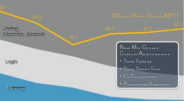
Click to Enlarge
200mm recovery and retooling creates opportunity. MPY = millions/year.
(Source: iSuppli, Applied Materials)


Giles Humpston, Tessera Inc.

Modern semiconductors are manufactured with feature sizes measured in nanometers. Despite this, semiconductors are not traditionally classed as nanotechnology. A transistor made with 0.5µm technology does not behave in a manner greatly different to one at the 32nm node. To fit with the modern definition of nanotechnology, materials must exhibit properties that are different from those predicted by simple scaling of dimensions. Their properties are influenced by the laws of physics because the feature size is of the same order as the critical size for physical phenomena. Often the difference is manifest as a step change. For example, the radius of the tip of a crack is typically tens of nanometers. Conventional crack propagation and consequent mechanical failure are impossible if the material dimensions are smaller than this.

Nanotechnology is likely to manifest itself in the semiconductor industry in two forms. The first of these is semiconductor devices themselves. It is well known that we cannot go on shrinking devices ad infinitum. Once the device size approaches single atoms quantum physics comes into play — a transistor may, or may not, switch, depending on the prevailing statistics. Building traditional logic gates out of such devices is not sensible, but other decision-making architectures based on quantum devices are being developed. For solid state memories, an important metric of the material used is the ratio of change between the 1 and 0 states. In a well-designed and fabricated flash memory, the ratio will be around 10,000. By exploiting phase change in the nanomaterial graphene, it is possible to obtain ratios of conductivity over 1 million. If realized in a full-sized memory, this would result in a five-fold increase in storage capacity.

In the near term, the most likely application of nanotechnology to semiconductors is in the area of interconnects. Most recent research effort has been concentrated on carbon nanotubes (CNTs). These materials are ballistic conductors with quantum behavior and exhibit exceptionally low electrical resistance. Values around 10E-4 Ohm-cm have been measured, and they have stable current densities as high as 10E12 A/cm2. One of the major causes of power consumption and propagation delay in semiconductor circuits is the RC time constant of interconnects; reducing R by a factor of 10 will confer significant benefits to conventional semiconductors.

Nanotechnology may even replace the ubiquitous gold plating found on the connectors of virtually every plug-in card. Gold is an excellent conductor, but needs to be a minimum thickness to adequately resist corrosion and add durability. The recent spike in the price of gold is having a measurable effect on connector pricing. Nanomaterials are under development that essentially mimic the electrical and mechanical properties of gold. Because they are base metal alloys, their prices are low and remain stable.

It has been said that the twentieth century was the era of the electron, and the twenty-first century will be the era of the photon. USB3, with its optical interface, is an example of this transition. Nanotechnology, by virtue of its dimensions, is conducive to interacting with light. A well-known example is the quantum dot, one use of which is wavelength conversion. These offer the prospect of designing light-emitting semiconductors with high electro-optic efficiency, and changing the emitted light to the desired spectrum using an engineered coating.

Conclusion

Although there are few examples of commercialized semiconductor nanotechnology, there is no doubt that it offers the prospect of significant innovation by providing materials with properties outside of the current domain. The semiconductor industry, with its large and focused R&D base, is likely to be an early adopter. Research journals abound with papers on nanotechnology, offering a tantalizing glimpse of what the future may hold.

Giles Humpston received his PhD and BSc from Brunel U., U.K. and is director of Research and Development at Tessera, 3025 Orchard Parkway, San Jose, CA 95134 USA; [email protected].

March 23, 2011 – BUSINESS WIRE — BioNanomatrix Inc., a developer of nanoscale, single-molecule imaging and analysis platforms designed to reduce the time and cost needed to analyze the genome, has closed a $23.3-million Series B round of equity financing.

Domain Associates, based in Princeton, NJ, and San Diego, CA, led the round, with new investor Gund Investment Corporation and existing investors Battelle Ventures, Innovation Valley Partners and KT Venture Group joining the round.

The company is moving toward commercialization of its nanoAnalyzer platform for whole genome analysis, said R. Erik Holmlin, newly elected president and chief executive officer of BioNanomatrix.

Holmlin noted that BioNanomatrix introduced the nanoAnalyzer 1000 System at the 2010 annual meeting of the American Society of Human Genetics last November and said that the company "has already placed a number of systems with early-access users." Learn more about nanotechnology for life sciences/biomedical applications here.

"BioNanomatrix has made impressive progress in developing and refining its platform technology and testing the nanoAnalyzer in collaboration with leading researchers in the genomics field," said Domain Associates Partner Brian K. Halak, PhD., who joins the company’s Board of Directors.

"This capital infusion enables BioNanomatrix to establish a strong West Coast presence that will provide additional business opportunities and the ability to recruit from a talent base that has established this industry," Dr. Halak continued.

The nanoAnalyzer technology targets integration of genetic information in molecular diagnostics, personalized medicine and biomedical research.

BioNanomatrix is developing and commercializing technologies for analysis of large biological molecules, such as nucleic acids, which are vital to life science research, clinical diagnostic applications and development of new therapeutics. For more information, visit www.bionanomatrix.com.

Follow Small Times on Twitter.com by clicking www.twitter.com/smalltimes. Or join our Facebook group

By Debra Vogler, senior technical editor

March 23, 2011 — Emerging LED test standards was one of the topics covered at MEPTEC’s The Heat is On event, held in CA this week. András Poppe, PhD, marketing manager in Mentor Graphics’ MicReD division, took on a number of important LED testing challenges in his presentation.

Listen to Vogler’s interview with Poppe:  Download or Play Now 

The importance of defining thermal resistance for LEDs was noted by Poppe: some LED vendors neglect the effect of radiant flux (Popt, i.e., emitted optical power) in their calculations, which results in better data than is actually achieved in the field. Still another example where calculations need to be carefully weighed is determining the amount of cooling needed for reliable LED operation (Fig. 1). In this case, hot lumens need to be taken into account, essentially, calculating the light output under real operating junction temperatures (i.e., the actual operating conditions) rather than laboratory test conditions. In the accompanying podcast interview, Poppe explains these concepts.

Junction temperature — performance indicator Differential formulation of the thermal resistance

Calculation: TJ = RthJ-X x PH + TX 
RthJ-X junction-to-reference_X thermal resistance supplied by the LED vendor
PH heating power measured/calculated by the LED user. How?
TX reference temperature (un)specified by the LED user.

Used in the design process to decide if the foreseen cooling is sufficient or not.
Not enough: in case of LEDs, prediction of "hot lumens" is also required.

 Click to Enlarge
Figure 1. Junction temperature and thermal resistance calculations. SOURCE: Mentor Graphics

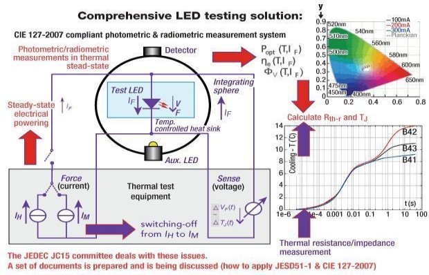
Poppe also presented a comprehensive LED testing solution (Fig. 2), noting that the JEDEC JC15 committee is working on this issue along with the CIE (Commission Internationale de l’Eclairage). Additional comments can be heard in his interview, along with a discussion of challenges associated with testing AC mains-driven LEDs — a major trend because they can be substituted for conventional light bulbs.


Click to Enlarge

Figure 2. Comprehensive LED testing. SOURCE: Mentor Graphics

Subscribe to Solid State Technology/Advanced Packaging.

Follow Solid State Technology on Twitter.com via editors Pete Singer, twitter.com/PetesTweetsPW and Debra Vogler, twitter.com/dvogler_PV_semi.

Or join our Facebook group

March 23, 2011 – Marketwire — Supertex Inc. (NASDAQ: SUPX), high voltage analog and mixed signal integrated circuits (ICs) maker, will package its HV2601 and HV2701 16-channel, low-charge injection, 200V analog switch ICs in 5.29 x 5.30mm, 42-ball bumped die packages. This packaging represents a 50% space savings over the previous 48-ball fpBGA package (28 sq. mm vs. 56 sq. mm).

These ICs suit space-limited applications that require high voltage switching controlled by low voltage signals, such as in portable and handheld medical ultrasound imaging systems. They feature very low quiescent current of 10µA, 22 ohm switch resistance, up to 200V operating voltage, and a serial shift register control. The HV2701 also features integrated bleed resistors for minimized noise and reduced capacitive coupling.

"As the size of medical ultrasound imaging systems continues to shrink, manufacturers are seeking ways to increase board density without sacrificing performance," states Stephen Lin, VP of marketing for Supertex. "Supertex’s HV2601BD and HV2701BD answer this need by offering system designers sixteen channel switching with a footprint that’s half the size of the previously available option."

HV2601 and HV2701 are available in a 42-ball bumped die package (HV2601BD and HV2701BD) in addition to the previously available 48-lead LQFP package (HV2601FG-G and HV2701FG-G). The parts are RoHS compliant.

Supertex Inc. is a publicly held mixed signal semiconductor manufacturer, focused in high voltage analog and mixed signal products for use in the medical, LED lighting, imaging, industrial, and telecommunication industries. Learn more at www.supertex.com.

Subscribe to Solid State Technology/Advanced Packaging.

Follow Advanced Packaging on Twitter.com by clicking www.twitter.com/advpackaging. Or join our Facebook group