Category Archives: LEDs

February 10, 2011 – Marketwire — SPP Process Technology Systems (SPTS), plasma etch, deposition, and thermal processing equipment manufacturer for the micro-device industry, completed the acquisition of deep reactive ion etch (DRIE) technology and certain related assets from Tegal Corporation. In addition, the deal includes the transfer to SPTS of the capital stock and operations of Tegal France SAS, a wholly-owned Tegal subsidiary formed by Tegal’s acquisition of Alcatel Micro Machining Systems’ DRIE assets in September 2008.

SPTS’ acquisition will include the Tegal DRIE product line (including 200, 110, 3200, and 4200 series), along with the Compact and Pluto development assets, intellectual property (IP) and process know-how. SPTS will provide continued global support to existing Tegal DRIE customers, and will integrate these technologies into its SPTS’ broad range of product offerings in etch, deposition and thermal technologies. SPTS just days ago acquired the etch portfolio of Primaxx from its parent company.

"The sale of the Tegal DRIE assets to SPTS secures our technology, team members, active joint development projects in France, and ensures continuation of our commitments to customers globally," said Thomas Mika, president and CEO, Tegal Corporation. "This event represents another major step in Tegal’s transformation from semiconductor capital equipment supplier to its new role in providing green energy." Tegal recently announced participation in the formation of sequel Power, a company engaged in large scale photovoltaic (PV)-based solar utilities.

SPP Process Technology Systems was established in October 2009 as the vehicle for the merger of Surface Technology Systems and acquired assets of Aviza Technology. The company is a wholly-owned subsidiary of Sumitomo Precision Products Co., Ltd., and designs, manufactures, sells, and supports advanced semiconductor capital equipment and process technologies for the global semiconductor industry and related markets. These products are used in a variety of market segments, including R&D, data storage, MEMS and nanotechnology, advanced 3-D packaging, LEDs, and power integrated circuits for communications. For more information about SPTS, please visit www.spp-pts.com.

Tegal is dedicated to the development and application of both proven and emerging technologies in the field of green energy. Tegal is engaged in the promotion of solar power plant development projects worldwide, the development of self-sustaining businesses from such projects, including supporting, developing, building and operating solar photovoltaic fabrication facilities and solar farms and other non-PV based renewable energy projects. Learn more at www.Tegal.com.

Subscribe to Solid State Technology/Advanced Packaging.

Follow Solid State Technology on Twitter.com via editors Pete Singer, twitter.com/PetesTweetsPW and Debra Vogler, twitter.com/dvogler_PV_semi.

Or join our Facebook group

LED measurement webcast


February 8, 2011

February 8, 2011 — On March 2, 2011, Solid State Technology and LEDs Magazine will co-host "Light and Color Measurement of Today’s LED Technology," a free webcast sponsored by Konica Minolta Sensing Americas. The company’s presenters will provide in-depth information on optical measurement techniques of LED technology, such as lighting, color theory, and LED structure.

Topics covered will include:

  • light theory
  • color theory
  • LEDs and optical emission
  • measurement devices
  • measurement types & applications specific measurements
  • and measurement results & interpretation

Attendees at the live event can participate in a Q&A with the applications engineers after the program. The free webcast will take place on March 2 at 2PM EST and is expected to run about one hour. Registrants can choose to participate in the live event or view the webcast at any time on-demand. Register for "Light and Color Measurement of Today’s LED Technology" here.

The seminar is designed to enable attendees to characterize and communicate the light and color properties of LEDs accurately.

Speakers:
Jay Catral majored in Electronics Engineering with a minor in Communications at De La Salle University in Manila Philippines. His career begin in 1992 with Minolta’s photographic division and in 2002 moved to what was then Konica Minolta’s Instrument Systems Division as a master technician for the service department. Currently Jay is the technical sales and applications manager for the Eastern United States.
 
Joe Esteves began his career 6 years ago with what was then known as Konica Minolta’s Instrument Systems Division as a master repair engineer for the service department. He has a deep technical understanding of measurement hardware as well as lighting applications experience. Currently Joe is the special accounts manager/technical application specialist for the western region of the United States.

Konica Minolta Sensing Americas Inc. provides optical test and measurement solutions for applications in Universities, Research and Development Laboratories, Food, Plastics, Paint and Coatings, Transportation, Textiles, Medical, Pharmaceutical, Agricultural, Architecture, Archeology, Animation, etc. Learn more at www.konicaminolta.com

Subscribe to Solid State Technology/Advanced Packaging.

Follow Solid State Technology on Twitter.com via editors Pete Singer, twitter.com/PetesTweetsPW and Debra Vogler, twitter.com/dvogler_PV_semi.

Or join our Facebook group

February 4, 2011 — During the past ten years, Clarkson University has received more than $1.4 million of direct and indirect (through Semiconductor Research Corporation) funding from Intel Corporation.

Intel donated silicon wafer polishing equipment and provided the funding to support research in the area of chemical-mechanical planarization (CMP) to Professors S.V. Babu, Egon Matijevic, and Dipankar Roy, and in nanoparticle detachment to Prof. Cetin Cetinkaya.

The money also supported many graduate and undergraduate researchers, and led to the hiring of 12 Clarkson Ph.D. graduates in recent years.

Intel is a global leader in silicon innovation and the world’s largest manufacturer of microprocessors. Learn more at www.intel.com

Located just outside the Adirondack Park in Potsdam, N.Y., Clarkson is a nationally recognized research university for undergraduates in engineering, business, arts, sciences and health sciences. Learn more at www.clarkson.edu

Subscribe to Solid State Technology/Advanced Packaging.

Follow Advanced Packaging on Twitter.com by clicking www.twitter.com/advpackaging. Or join our Facebook group


By Debra Vogler, senior technical editor

February 3, 2011 — With GT Solar’s acquisition of Crystal Systems in 2010, the company made a decision to break into large substrates for the LED market. GT Crystal Systems’ COO, Kurt Schmid provides details about the company’s directional solidification process based on the heat exchanger method, in which the seed is at the bottom, thereby forcing impurities away from the solid as the material solidifies (see Figure). Bubbles (and other impurities and dislocations) are forced to move up; the result is a large ingot with low bubble content, high purity levels, and a very uniform crystal structure that lends itself to the deposition of materials such as GaN. According to the company, this process is very controlled and low stress.

Click to Enlarge

Figure. Sapphire growth process. SOURCE: GT Crystal Systems

Schmid spoke with ElectroIQ.com’s Debra Vogler, senior technical editor, at Photonics West, January 22-27, 2011, in San Francisco. Listen: Download (iPhone/iPod users)  or Play Now

If the LED market is to continue to thrive, Schmid observes that wafer manufacturers using MOCVD equipment will need to move to traditional semiconductor manufacturing technologies, which are based on 6"-diameter and larger size substrates. Such a move translates to using more automation, which goes hand-in-hand with efforts to lower the price of LEDs. Schmid anticipates additional potential markets will open up as LED prices decrease, and performance improves.

Subscribe to Solid State Technology/Advanced Packaging.

Follow Solid State Technology on Twitter.com via editors Pete Singer, twitter.com/PetesTweetsPW and Debra Vogler, twitter.com/dvogler_PV_semi.

Or join our Facebook group

February 3, 2011 — The New Hampshire Innovation Commercialization Center (NH-ICC) has attracted a $100,000 grant from the New Hampshire Innovation Research Center (NHIRC) to help commercialize semiconductor technology developed by Durham, NH-based startup Innovacene. Innovacene was founded last year by University of New Hampshire (UNH) professor Glen Miller to commercialize the semiconductor technology he and his research team developed at UNH’s Center for High-rate Nanomanufacturing in Durham. The company has created an extremely thin, organic, ultra-lightweight surface-emitting semiconductor coating for use in organic light-emitting diodes (OLEDs), according to a press release sent to Mass High Tech.

OLEDs are currently used in light-emitting screens for devices such as mobile phones and computers. Innovacene’s technology would allow manufacturers to apply the coating to large surfaces, such as wallpapers and ceiling tiles, to create a more natural style of lighting.

According to Miller, the company will use the grant funding to develop these ultra-high efficiency lighting products, which will be inexpensive to install and able to be manufactured at high rates.

"These products will produce the highest quality natural white light while consuming a fraction of the energy associated with conventional white lighting products," said Miller.

The company has partnered with the NH-ICC to develop a comprehensive business plan while developing prototype devices, Miller said . They will also be working to identify financing options so that Innovacene can grow quickly to meet the needs of the emerging OLED lighting market.

Mark Galvin, NH-ICC manager director, said the NH-ICC helped with Innovacene’s grant request because of the unique differentiations in the company’s early prototypes. With the correct resources over the next year or so, said Galvin, those differences should allow successful commercialization of Innovacene’s OLED technology. Galvin said he hopes that Innovacene will eventually become a resident of the NH-ICC.

Located at the Pease Tradeport in Portsmouth, the NH-ICC was launched last year by Galvin, a veteran in the telecom industry who founded Cedar Point Communications in Derry, N.H. and Whaleback Systems Corp. in Portsmouth, N.H. 

Learn more about MassHighTech’s story at www.masshightech.com/stories/2011/01/24/daily39-UNH-startup-Innovacene-receives-100K-grant-with-help-from-NH-ICC.html 

February 2, 2011 — Helios Crew Corporation (HCC) Taiwan released its LED product S35, a packaged component light-emitting diode (LED) that integrates MEMS with semiconductor processing to produce a unique silicon packaging technology.

Click to EnlargeIn conjunction with a high-brightness SemiLEDs chip, this compact size, silicon sub-mount technology delivers brightness and reliability. In addition, the S35 silicon has a thermal conductance more than 8 times higher than aluminum oxide ceramic packages, and at a considerably lower cost than aluminum nitride ceramic.
Helios Crew, Corporation is a subsidiary of SemiLEDs, Inc., a USA LED chip manufacturer traded on Nasdaq under the symbol LEDS. Learn more at www.helioscrew.com

Follow Small Times on Twitter.com by clicking www.twitter.com/smalltimes. Or join our Facebook group

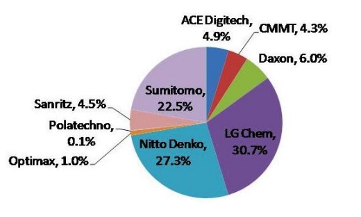
February 1, 2011 — Displaybank, market research and consulting provider for the display industry, reports that LG Chemical secured its number one position in the large-area TFT-LCD polarizer market for the second straight year. LG Chemical has 30.7% market share, followed by Nitto Denko with 27.3% share and Sumitomo Chem. with 22.5% share. For the large-area TFT-LCD polarizer market in 2010, these top 3 suppliers’ market share exceeded 80% of the total market. These and other findings are disclosed in Displaybank newly updated "Polarizer and Optical Films Industry Trend Analysis," which covers global polarizer market in detail on a quarterly basis.

Click to Enlarge
Figure 1. Large-area TFT-LCD polarizer market share by maker (Area-basis, Y2010). Source: Polarizer and Optical Films Industry Trend Analysis, Displaybank January 2011.

As value-added polarizer demand rises including polarizer for LEDs, 3D, and touch panel displays, market share for these top 3 makers shows continuous growth. Irene Heo, senior analyst at Displaybank, noted "the industry dependence towards these top 3 polarizer makers will continue to go up in 2011, as the makers have manufacturing know-how for value-added films and also secure higher price competitiveness against other makers."

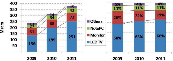
Area basis (Msqm) 2009 2010  2011   Revenue basis (USD million) 2009 2010 2011
 LCD TV 136  199  251     LCD TV 3,488  4,946  5,670
Monitor  61  68  72     Monitor  1,884  2,084  2,092
Notebook PC 27 34 42   Notebook PC  864   1,068 1,221
Others 13 14 15   Others 991 1,090 1,162
Total 236  315  380     Total  7,227  9,188  10,145
Tables. Polarizer markets by major application. Source: Polarizer and Optical Films Industry Trend Analysis, Displaybank January 2011.

As new line operation and decreased demand during 2H 2010 led to a drop in polarizer price, the overall polarizer market in 2010 is estimated at $9.18 billion, slightly lower than previous expectation. In terms of area-basis, the market is estimated to have grown 24% from 2009 to 320 million square meters in 2010.

Click to Enlarge
Figure 2. Polarizer market forecast by application (Area-basis). Source: Polarizer and Optical Films Industry Trend Analysis, Displaybank January 2011.

By major application, TV-use polarizer market reached $4.95 billion (54% of applications) in 2010; monitor-use polarizer use  hit $2.08 billion; notebook-use polarizers reached $1.07 billion. In terms of area-basis, TV-use polarizer reached 200 million square meters: 63% of the total market.

Heo noted "in 2011, large-area polarizer market is expected to exceed $10.1B to grow 10.4% Y/Y and TV-use and notebook-use polarizer will each grow 14.6% and 14.3% Y/Y respectively."

Access "Polarizer and Optical Films Industry Trend Analysis" at http://www.displaybank.com/eng/report/report_show.php?id=15

Displaybank is a global authority in market research and consulting for the electronic display industry. Displaybank’s analysts are located throughout Korea, Japan, China, Taiwan, and the U.S. For more information, visit www.displaybank.com.

Follow Solid State Technology on Twitter.com via editors Pete Singer, twitter.com/PetesTweetsPW and Debra Vogler, twitter.com/dvogler_PV_semi.

Or join our Facebook group

February 1, 2011 – Eulitha AG and Dai Nippon Printing (DNP) say they have successfully patterned 4-in Si wafers with Eulitha’s "PHABLE" technology, creating uniform photonic crystal patterns with 600nm period and hexagonal symmetry.

The PHABLE ("Photonic Enabler") is a mask-based UV lithography technology that enables formation of periodic nanostructures over large areas, forming an image with a very large depth-of-focus (the company has called it "practically unlimited") to accommodate patterning on even nonflat substrate surfaces. Combinations of different patterns (e.g. hexagonal or square grids) can be printed using a single exposure, with feature resolution as small as a 1/4 of the illumination wavelength.

Achieving uniform patterning on 4-in. wafers (using a DNP high-resolution mask on standard quartz/Cr plate) is an important milestone, the companies say. HB-LED makers are moving up to the next bigger wafer sizes (4-in. and 6-in.). Photonic crystal structures that enhance LED light extraction, or patterned sapphire substrates, can be fabricated with the PHABLE technology — as can required substrates for nanowire-based LED or solar-cell applications.

Click to EnlargePete Singer
Editor-in-Chief

The market for high brightness light-emitting diodes is exploding, largely driven applications in displays, signage and general illumination. According a report from PennWell’s Strategies Unlimited, the HBLED market is projected to grow 29.5% per year, reaching over $19 billion by 2014. The application with the highest forecast growth rate is signs/displays, with a CAGR of 60.6% (this includes LED-based TVs).  Illumination has the next-highest growth rate, with a projected CAGR of 45.4%. 

The LED manufacturing process is somewhat similar to mainstream semiconductor manufacturing, in that it involves a substrate (either sapphire or GaN), deposition of a fairly complex epitaxial structure (by metal organic chemical vapor deposition, MOCVD), followed by wafer processing (contact formation, etch, thinning), die separation and packaging.

As in mainstream semiconductors, the cost of high volume LED production must continually be reduced, both at the chip and packaged device level. We’ll be exploring that in-depth later this month, at the Strategies in Light conference, Feb. 22-24 at the Santa Clara convention center. A four-hour workshop, which I’ll be moderating, will focus on advances in LED manufacturing technology that will be needed to reduce the cost of HB LEDs (to be held Tuesday, Feb. 22nd, 8:00 am -12:00 noon).

Our speakers will be James Brodrick, manager of the solid-state lighting program at the U.S. Department of Energy; Bill Quinn, chief technologist of Veeco’s MOCVD operations; Ravi Kanjolia, chief technology officer of SAFC Hitech; Thomas Uhrmann, business development manager at EVG; Chris Moore, President and CEO of Semilab AMS; and, from Rudolph Technologies, Mike Plisinski, vp and general manager, and Ardy Johnson, vp of corporate marketing.

As with logic and memory devices, LED market growth is largely driven by advances in performance – in this case LED efficiency, measured in lumens/Watt – and reductions in cost. Higher efficiencies are possible through chip design, light extraction technology, packaging methods and driver performance. Costs are a function of the number of LEDS per light output, manufacturing equipment performance/productivity, materials use and, of course, yield.

A roadmap for manufacturing R&D has also been created. Published in July of 2010, the "Solid-State Lighting Research and Development: Manufacturing Roadmap" calls out specific challenges for luminaires, LEDs and OLEDs. The seven big challenges for the first two:

  • Luminaire/Module Manufacturing: Automation, manufacturing and design tools for high quality, flexible manufacturing at low cost
  • Driver Manufacturing: Improved design for manufacture for flexibility, reduced parts count and cost, while maintaining performance
  • Test and Inspection Equipment: High-speed, non-destructive, and standardized equipment
  • Tools for Epitaxial Growth: Tools, processes and precursors to lower cost of ownership and improve uniformity
  • Wafer Processing Equipment: Tailored tools for improvements in LED wafer processing
  • LED Packaging: Improve back-end processes and tools to optimize quality and consistency and to lower cost
  • Phosphor Manufacturing and Application: High volume phosphor manufacture and efficient materials application.

Of these tasks, the first two are associated with luminaire manufacturing, and the last four with the LED chip and package. Test and inspection applies to both. Similar challenges exist for OLEDs:

  • OLED Deposition and Patterning Equipment: Equipment for high speed, low cost, uniform deposition, and/or patterning of OLED structures and layers.
  • Integrated Manufacturing and Quality Control: Methods to integrate the many process steps, to check the quality and compatibility of materials.
  • OLED Materials Manufacturing: Advanced manufacturing of organic and inorganic OLED materials
  • Back-end Panel Fabrication: Tools and processes for manufacturing OLED panels from OLED sheet material.

While LED manufacturing is similar to that of mainstream semiconductors, it’s perhaps more akin to photovoltaics manufacturing: There are many competitors with similar processes, margins are slim and China has been aggressively building a manufacturing infrastructure.

More Solid State Technology Current Issue Articles
More Solid State Technology Archives Issue Articles


By Debra Vogler, senior technical editor

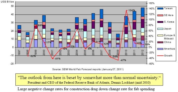
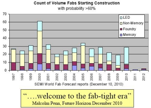
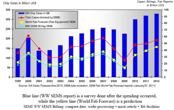
January 24, 2011 — Speaking at SEMI’s Industry Strategy Symposium (ISS) in January, Christian Dieseldorff, SEMI’s senior analyst, provided an in-depth look at fab construction, capacity, and capex in 2011 and 2012 (see figures).

Listen to Dieseldorff’s interview:  Download for iPhone/iPod users  or Play Now

In this podcast, Dieseldorff walks listeners through fab construction projects by region and device type (LED, non-memory, memory, etc.). He speaks with Debra Vogler, senior technical editor.

Click to Enlarge

Figure 1. Fab spending on front end facilities (Construction and equipping, including discretes). SOURCE: SEMI

Dieseldorff sees a decline in construction projects in 2011, followed by a double-digit decline in projects in 2012.

Click to Enlarge

Figure 2. Fab construction projects: Count of fabs vs. type. SOURCE: SEMI

Breaking out LED fabs, Dieseldorff notes that the largest growth regions (capacity and number of participating companies) are China, Taiwan and Korea. For 2011 and 2012, however, there aren’t many new LED fabs. 

Click to Enlarge

Figure 3. Equipping fabs — chip sales & capex trends: Both riding the same rollercoaster. SOURCE: SEMI

Subscribe to Solid State Technology/Advanced Packaging.

Follow Solid State Technology on Twitter.com via editors Pete Singer, twitter.com/PetesTweetsPW and Debra Vogler, twitter.com/dvogler_PV_semi.

Or join our Facebook group