Category Archives: LEDs

(August 9, 2010) — A Europe-wide consortium has taken up the challenge of making a significant impact on the power consumption of telecommunications and data networks, which are estimated to consume as much as 3% of European electricity. Five partner organizations have come together in the BIANCHO project (BIsmide And Nitride Components for High temperature Operation), a 3-year research and development initiative supported by €2.190 million through the EU Framework 7 program.

The project will develop new semiconductor materials to allow lasers and other photonic components to become more energy efficient and also more tolerant of high operating temperatures. This power reduction is vital as optical communication systems are becoming the principal way to deliver ever-increasing data-rich broadband services to homes and businesses.

Follow Solid State Technology on Twitter.com via editors Pete Singer, twitter.com/PetesTweetsPW and Debra Vogler, twitter.com/dvogler_PV_semi. Or join our Facebook group

Many current photonic components for telecommunications applications have major intrinsic losses, with around 80% of the electrical power used by a laser chip being emitted as waste heat, for example. The presence of this waste heat necessitates the use of thermo-electric coolers and an air-conditioned environment in order to control the device temperature, cascading the energy requirements by more than an order of magnitude.

The energy losses are mainly due to a process known as Auger recombination, a consequence of the band structure of the semiconductor materials used in making components such as semiconductor lasers and optical amplifiers. Over many years, incremental approaches have sought to reduce the consequent inefficiencies without addressing their fundamental cause. BIANCHO proposes a radical change of approach: to eliminate Auger recombination by manipulating the electronic band structure of the semiconductor materials through the use of novel dilute bismide and dilute nitride alloys of Gallium Arsenide and Indium Phosphide. This will allow the creation of more efficient and temperature tolerant photonic devices which could operate without the power-hungry cooling equipment that today’s networks demand.

The project brings together five leading European partners with complementary expertise in epitaxy, structural characterization of materials, device physics, band structure modelling, advanced device fabrication, packaging and commercialization. Coordinated by the Tyndall National Institute (Ireland), internationally recognized for its strength in semiconductor band structure modelling, the other academic partners are Philipps Universitaet Marburg (Germany) focussing on material growth and characterization; Semiconductor Research Institute (Lithuania) responsible for the design, manufacture and characterization of bismide-based epitaxial structures; the University of Surrey (UK) who contribute unique characterisation facilities and modelling expertise. Commercialization of the project results will be led by CIP Technologies (UK) an organization with a long history of applied photonics innovation, particularly in the telecommunications sector.

Further information:

Tyndall National Institute – www.tyndall.ie/ptg
Contact: Mary O’Regan ([email protected]) Tyndall National Institute is the largest ICT-related research institute in Ireland. Tyndall covers a broad range of research capabilities in the areas of photonics, electronics and nanotechnology as well as related technological areas such as the interface between the Life Sciences and ICT.

Philipps University Marburg – www.uni-marburg.de/wzmw/strl
Contact: Professor Kerstin Volz ([email protected])
The Material Sciences Center (WZMW) of Philipps University Marburg (UNIMAR) is an interdisciplinary research centre founded in 1988. It encompasses groups from the departments of physics, chemistry and pharmacy and is engaged with research as well as with teaching in the respective departments. The structure and technology research laboratory (http://www.uni-marburg.de/wzmw/strl) deals mainly with the growth and characterisation as well as processing of and the application of III-V semiconductor heterostructures.

University of Surrey – www.surrey.ac.uk
The University of Surrey is one of the UK’s leading professional, scientific and technological universities with a world class research profile and a reputation for excellence in teaching and research.

Center for Physical Sciences and Technology, Semiconductor Physics Institute
Contact: Professor Arunas Krotkus ([email protected]) Semiconductor Physics Institute (http://www.pfi.lt/index_e.html ) is the largest research institute dealing with semiconductor technology, material and device investigations in Lithuania and in the Baltic countries.

CIP Technologies – www.ciphotonics.com
Contact: Michael Robertson ([email protected])
CIP Technologies is the trading name of The Centre for Integrated Photonics Ltd, a world-renowned developer of advanced photonic hybrid integrated circuits and InP-based opto-electronic chips, devices, arrays and modules for the communications, defence and renewable energy markets.

(August 5, 2010) — After a workgroup session at SEMICON West 2010 in San Francisco, the Docking and Mounting Interface Workgroup summarized its key goals. These include supply chain management and better time to market. Multitest’s business unit manager Günther Jeserer led the discussion.

The majority of attendees were suppliers of final semiconductor test equipment. Several equipment users, such as IDMs and test houses, also attended the workgroup and expressed their commitment. The workgroup defined the general goal of its activities as follows: 

  • Improve time to market
  • Improve efficiency and save cost 
  • Ease supply chain management

These targets must be achieved by reducing the complexity of the communication between equipment users and vendors, as well as minimizing the danger of miscommunication and communication errors.

Based on the recent workgroup, the next steps will be to work on standard terminology and reference points for the mechanical interfaces of probers, handlers, testers, dockings, contactors and load boards. All companies that use or supply test equipment are invited to actively contribute. A similar session will be held during SEMICON Europe in October 2010.

For more information about the Collaborative Alliance for Semiconductor Test (CAST), visit www.semi.org/cast

Read more about semiconductor test probes, handlers, and related equipment:

Multitest intros contactors for ICs with differential signals

MicroProbe debuts MEMS-based, multi-DUT, ultra-fine-pitch probe card for IC wafer test

Kelvin measurement using spring probes for packaged IC testing

(August 4, 2010 – BUSINESS WIRE) — CHAD Industries developed wafer-handling capabilities for Sapphire wafers used in the LED market.

As production demand increases for LED production, more and more OEM manufacturers are being asked by the end user to provide fully automated solutions for their process tool. CHAD has adapted the standard WaferMate200 workcell to handle the smaller 2”, 4”, and 6” sapphire wafer requirements.

Follow Solid State Technology on Twitter.com via editors Pete Singer, twitter.com/PetesTweetsPW and Debra Vogler, twitter.com/dvogler_PV_semi. Or join our Facebook group

“We have developed a standard suite of tooling options to permit a wide range of LED applications using our standard WaferMate200 platform,” says Scott Klimczak, president of CHAD Industries. “CHAD can provide all of the customization so that our customer’s OEM process tool can remain standard. This approach allows our OEM customers in the LED market to concentrate on their core competency (the process tool), and allows CHAD to concentrate on our core competency in wafer automation.”

CHAD’s capabilities for handling smaller sapphire wafers was exhibited in their booth at the Semicon West 2010 show in San Francisco in July. CHAD’s WaferMate200 workcell was tooled to handle 2” sapphire wafers and was loading and unloading a Veeco Instruments Inc. 3D non-contact ContourGT-X8 inspection tool during a live demonstration.

The CHAD LED wafer handling solutions can be applied to process tools at different stages of manufacture and for different types of manufacture — including metrology inspection and measurement, stud bumping, and solder bumping for advanced packaging.

For more information, call Rich Munro at CHAD Industries at 714-938-0080.

(August 4, 2010 – BUSINESS WIRE) — Semtech Corp. (Nasdaq: SMTC), analog and mixed-signal semiconductor supplier, announced the SC442, its first 10-channel white LED driver with an integrated 3A boost power switch. The device is capable of driving up to 120 LEDs at up to 30mA per channel and is packaged in an ultra-small, low-profile 4x4x0.6mm, 28-pin MLPQ package.

The high-density package, small external filter components, wide operating voltage range and high efficiency satisfy space constrained LED backlights serving LCD monitors and LCD-TVs. The high density LED driver is also ideal for ultra-bright displays exceeding 500Nits which serve medical, industrial, avionics and navigation markets, as well as digital signage applications. 

Follow Advanced Packaging on Twitter.com by clicking www.twitter.com/advpackaging. Or join our Facebook group

The device extends Semtech’s popular SC44x LED driver platform to address large LCD backlighting applications. The SC442 operates across a wide input voltage range of 4.5V to 21V for use with lithium ion battery packs or regulated 5V, 12V or 18V power supplies. The SC442 is capable of up to 42V output for driving up to 12 white LEDs per channel. The device is compatible with boost (step-up), or SEPIC (step-up/down) topologies. It also transitions seamlessly to bypass (or linear) mode; when the input voltage is greater than the output voltage. The synchronization feature eliminates inter-modulation noise found in backlight systems utilizing multiple driver ICs — such as those found in large LED backlit LCD-TVs. Other features include over-temperature, overload, open and programmable short LED protection.

“LCD system designers are seeking the largest, brightest viewing area with the smallest possible impact on chassis size and system heat,” said Steve Hawley, Semtech Product Marketing Manager for LED Lighting and Displays. “The SC442 provides significant illumination, low losses and a small solution size for next generation, large format and high brightness LCD displays.”

Up to 50kHz PWM dimming eliminates audio noise problems. The optimum LED output voltage is maintained dynamically by the internal DC-DC current mode controller. Channels can also be independently disabled for smaller panel designs. Open LED and programmable shorted LED protection as well as over-temperature are provided. The controller switching frequency is programmed from 200kHz to 1MHz to optimize efficiency and L/C filter sizing.

The SC442 LED driver is packaged in an MLPQ-UT 28-pin package with exposed thermal pad for excellent heat sinking. The SC442 is lead-free, halogen-free and fully RoHS compliant.

Key Features of the SC442 include 4.5V to 21V VIN Range, up to 42V VOUT Range, Up to 30mA per Channel, Efficiency up to 91%, ±1% LED Current Matching, and more. The SC442 joins Semtech’s existing platform of LED backlight drivers, including the 6-channel SC440A, 4-channel SC441A/C and 3-channel SC443 devices.

Applications include HDTV and Notebook PC LCD Displays and Backlights.

Semtech Corporation is a supplier of analog and mixed-signal semiconductors for high-end consumer, computing, communications and industrial equipment. For more information, visit http://www.semtech.com.

The rule of three for CMP


August 1, 2010

Click to EnlargeMichael A. Fury,
Techcet Group, LLC, Del Mar, CA

In Boy Scouts, we learned "leaves of three, let it be" to avoid the irritation and embarrassment of poison ivy. In the semiconductor industry, we learned "every chip manufacturing supply chain will eventually stabilize at three suppliers." Since its implementation in volume production in 1989, CMP has been slow to conform. While pads and slurries each began under the rule "suppliers: one; not much fun," CMP equipment hovered near the Rule of Three from the beginning. There were some wild excursions in the number of equipment suppliers in the 1990s, but once Applied Materials came on the scene, albeit slowly at first, the Rule of Three was never seriously challenged. The number of CMP equipment tombstones is about what one would expect for a field touted for more than a decade as "the fastest growing process sector in the semiconductor manufacturing business."

The roller coaster ride for CMP slurries has been a bit more thrilling, if not frightening, at least for some. From a high of over 35 self-proclaimed semiconductor slurry suppliers, we still have 15 manufacturers that can each claim a measurable market share of qualified volume production, according to the Techcet Group 2010 CMP Consumables Critical Materials Report. This supplier base is supported by the variety of process types currently in production, new processes and material sets being developed, and by regional market demands, particularly in Asia. The Rule of Three has not taken effect because we keep changing the rules – what materials do we want to polish, what materials do we want to stop on, what kinds of devices are we making, where are we making them, what are the cost pressures that govern.

Another factor that has foiled the Rule of Three is that CMP slurry is a performance material. For all the loose talk in which we may indulge about commodity pricing of ILD slurry, the fact is that no two slurries are interchangeable without some extensive process re-qualification and adjustment of quality control set points throughout the fab. This gives rise to a lore of legacy supply incumbency – once you’re in, you’re in for life – but this old behavior is no longer bankable, as fabs become more savvy about point of use dilution, reduced slurry flow, and other cost-reduction strategies.

The CMP pad business has quite a different story to tell. Long dominated by Rodel, the supplier itself was swallowed by Rohm and Haas, and then again by Dow Chemical, all the time holding on to its >80% market share. Competing pad startups have come and gone, unable to navigate the patent minefields successfully, or upon qualifying in a fab, being told that they need to be bigger before volume fab production will be committed to their pad. Only Thomas West found a sustainable niche early on, and holds steady to this day, mostly with its quiet corner of the tungsten pad market.

Along the way, there have been several disruptive threats to the CMP pad status quo. 3M’s fixed abrasive pads have captured about half of the selective STI market, but have struggled to expand beyond this single niche. ECMP promised a kinder, gentler approach to copper polishing with a Nafion® membrane enclosing a copper removal electrolyte, but was unable to concurrently meet the dishing specs across the requisite range of feature sizes. It may have found a niche in the read/write head process, but not in the chip fab. SemiQuest’s button pad still looking for the right opportunity to break into the pack with its promise of superior edge exclusion capability.

None of this lends itself to a legitimate conclusion that the Rule of Three has asserted itself in the CMP pad business, but there are certainly signs that the market dynamics are morphing in the direction of Rule of Three behavior. Fab engineers and purchasing agents are committing polishers and wafers to new pad qualifications. Pad conditioner suppliers are devoting more resources toward characterizing their products with non-Dow pads. Investors are showing renewed confidence in the ability to compete successfully with Dow, with new investment rounds secured for innoPad and NexPlanar.

Given the inexact nature of market forecasting, this is good enough for me to believe that CMP pads will eventually yield to the Rule of Three, plus or minus.

Michael A. Fury, Ph.D. is a Director & Technology Analyst at Techcet Group, LLC; ph.: +1-415-395-6945;  [email protected]

More Solid State Technology Current Issue Articles
More Solid State Technology Archives Issue Articles

(July 23, 2010) — Shin-Etsu Silicones of America Inc., U.S. subsidiary of Shin-Etsu Chemical Co. Ltd., Japan, launched the TC-CA Series, comprised of Shin-Etsu’s advanced polymer and thermally conductive filler 

Figure 1. Heat dissipation for semiconductor devices.

composite material technologies. The low-hardness silicone soft pad series of products have both high thermal conductivity and excellent electrical insulation properties for package cooling.

The TC-CA Series also offers excellent cost-performance that meets the growing need for thinner and lighter weight electronic device applications such as those mounted in notebook PCs, LED lighting, hybrid cars and electric cars, etc. Additionally, the “soft pad” materials allow better line-to-line contact between the heat sink and the heat generating component which means more heat transfer−which equates to longer life parts.

Compared to conventional products, the new silicone soft pad product series offer a combination of advanced polymer and thermally conductive filler composite material properties including:

  • Low-hardness that makes for good compressibility;
  • Stress-relaxation property that can reduce stress to heat modules;
  • Excellent workability and processibility;
  • Low specific gravity

These heat-dissipating thermal interface materials (TIM) are thermally conductive compounds fitted between the heat-generating unit; such as a computer’s CPU, and the heat sink. Depending on the application, it is possible to meet diverse heat-dissipation requirements as each product in the series offers a combination of unique properties from which customers can choose the most appropriate product based on specific application or usage conditions.

Figure 2. Low-hardness thermally conductive silicone soft-pad TC-CA Series.

According to Shin-Etsu’s North America marketing manager Eric Bishop, “The TC-CA series meets the expanding demand for a thermally conductive solution for heat-dissipation applications in the growing number of electronic components in automobiles and LEDs−as well as in PCs, home appliances, and electronic game units. Moreover, due to the increasing miniaturization and higher performance of electronic devices, the need for more effective heat-dissipation materials is further increasing.”

A U.S. subsidiary of Shin-Etsu Chemical Co. Ltd., Japan, Shin-Etsu Silicones of America Inc. is a major supplier of silicone materials to North America’s medical, automotive, electronics, aerospace, and manufacturing industries.

Follow Advanced Packaging on Twitter.com by clicking www.twitter.com/advpackaging. Or join our Facebook group

(July 21, 2010) — The Institute of Microelectronics (IME), a research institute of the Agency for Science, Technology and Research (A*STAR), announced a collaborative partnership with Stanford University to develop silicon-nanowire-based circuits that are inspired by the brain. Under the research collaborative agreement, IME and Stanford will jointly develop silicon nanowire based neuromorphic computational elements (silicon neurons) that take advantage of the capabilities of nanowire technology.

The quest to come up with an artificial system organized like the biological nervous system promises to drive the future of humanoid robots and supercomputers that can perform highly complex decision-making for gaming and defense technologies. The electronics systems using neuromorphic designs aim to work like the biological nervous system. The collaboration represents a further expansion of the extensive neuromorphic computing activities at Stanford University and provides a new application opportunity for nanowire transistors developed at IME.

The partnership leverages on the relative strengths of the respective institute. IME is a leading laboratory in the fabrication of nanowire transistors, with considerable progress reported in recent years, including the demonstration of functional circuits. Stanford University has a leading group in neuromorphic engineering, an approach to designing systems that work like the brain.

The joint project will be led by Dr Navab Singh, Principal Investigator of the NanoElectronics section at IME, and Associate Professor Kwabena Boahen, Director of the Brains In Silicon group at Stanford University. The project will tap Stanford University’s expertise in neuromorphic design to model and design silicon neuron circuits.  The circuits will be fabricated by IME using state-of-the-art nanowire technology, more specifically, the lateral gate-all-around FUSI gate transistor technology.

“The gate all around (GAA) transistors based on silicon nanowires are considered the most promising alternatives to scaling limitations of planar CMOS technology — foundation of today’s electronics. Nanowire transistors offer near ideal subthreshold behaviour, low off state leakage, and high drive current — all the characteristics required to enable a highly integrated design that works with little power, much like the real brain. On the other hand, due to nanowire’s structure and strong response in respect to tiny change in dimension, nanowire transistors also exhibit increased variability, strong low frequency and telegraph-style noise that are interesting to niche applications,” said Dr Singh.

On the unique characteristics of nanowire transistors, Associate Professor Boahen said, “Our joint mission is to develop revolutionary architectures that would be tolerant to, or better yet, thrive under the variability and noise. Interestingly, variability and noise are key elements of a biological brain.”

Professor Dim-Lee Kwong, executive director of IME, said, “IME’s alliance with Stanford University to develop neuromorphic test circuits will be a window to the future of an emerging discipline that is expected to have a ripple effect on a broad spectrum of industries.”

The Institute of Microelectronics (IME) is a research institute of the Science and Engineering Research Council of the Agency for Science, Technology and Research (A*STAR) of Singapore. A*STAR oversees 14 biomedical  sciences, and physical sciences and engineering research institutes, and seven consortia & centre, which are located in Biopolis and Fusionopolis, as well as their immediate vicinity. For more information about A*STAR, visit www.a-star.edu.sg

Also read:

Fully gate-all-around silicon nanowire CMOS devices

Although CVD-grown nanowires are good for demonstration purposes, getting them into manufacturing calls for the utilization of CMOS fabrication methods … (Solid State Technology, 2008, Volume 51, Issue 5, co-authored by Dr. Navab Singh and Professor Dim-Lee Kwong)

Toshiba tips Si nanowires for 16nm chips

Presenting at the VLSI Symposium, Toshiba says it has developed a silicon nanowire transistor with vastly improved on-current levels, targeting 16nm and beyond system LSIs … (Small Times, 2010, online issue)

(July 14, 2010) — Rice University scientists have found the ultimate solvent for all kinds of carbon nanotubes (CNTs), a breakthrough that brings the creation of a highly conductive quantum nanowire closer.
 
Nanotubes have the frustrating habit of bundling, making them less useful than when they’re separated in a solution. Rice scientists led by Matteo Pasquali, a professor in chemical and biomolecular engineering and in chemistry, have been trying to untangle them for years as they look for scalable methods to make exceptionally strong, ultralight, highly conductive materials that could revolutionize power distribution, such as the armchair quantum wire.
 
The armchair quantum wire — a macroscopic cable of well-aligned metallic nanotubes — was envisioned by the late Richard Smalley, a Rice chemist who shared the Nobel Prize for his part in discovering the the family of molecules that includes the carbon nanotube. Rice is celebrating the 25th anniversary of that discovery this year.
 
Pasquali, primary author Nicholas Parra-Vasquez and their colleagues reported this month in the online journal ACS Nano that chlorosulfonic acid can dissolve half-millimeter-long nanotubes in solution, a critical step in spinning fibers from ultralong nanotubes.
 
Current methods to dissolve carbon nanotubes, which include surrounding the tubes with soap-like surfactants, doping them with alkali metals or attaching small chemical groups to the sidewalls, disperse nanotubes at relatively low concentrations. These techniques are not ideal for fiber spinning because they damage the properties of the nanotubes, either by attaching small molecules to their surfaces or by shortening them.
 
A few years ago, the Rice researchers discovered that chlorosulfonic acid, a "superacid," adds positive charges to the surface of the nanotubes without damaging them. This causes the nanotubes to spontaneously separate from each other in their natural bundled form.
 
This method is ideal for making nanotube solutions for fiber spinning because it produces fluid dopes that closely resemble those used in industrial spinning of high-performance fibers. Until recently, the researchers thought this dissolution method would be effective only for short single-walled nanotubes.
 
In the new paper, the Rice team reported that the acid dissolution method also works with any type of carbon nanotube, irrespective of length and type, as long as the nanotubes are relatively free of defects.
 
Parra-Vasquez described the process as "very easy."
 
"Just adding the nanotubes to chlorosulfonic acid results in dissolution, without even mixing," he said.
 
While earlier research had focused on single-walled carbon nanotubes, the team discovered chlorosulfonic acid is also adept at dissolving multiwalled nanotubes (MWNTs). "There are many processes that make multiwalled nanotubes at a cheaper cost, and there’s a lot of research with them," said Parra-Vasquez, who earned his Rice doctorate last year. "We hope this will open up new areas of research."
 
They also observed for the first time that long SWNTs dispersed by superacid form liquid crystals. "We already knew that with shorter nanotubes, the liquid-crystalline phase is very different from traditional liquid crystals, so liquid crystals formed from ultralong nanotubes should be interesting to study," he said.
 
Parra-Vasquez, now a postdoctoral researcher at Centre de Physique Moleculaire Optique et Hertzienne, Université de Bordeaux, Talence, France, came to Rice in 2002 for graduate studies with Pasquali and Smalley.
 
Study co-author Micah Green, assistant professor of chemical engineering at Texas Tech and a former postdoctoral fellow in Pasquali’s research group, said working with long nanotubes is key to attaining exceptional properties in fibers because both the mechanical and electrical properties depend on the length of the constituent nanotubes. Pasquali said that using long nanotubes in the fibers should improve their properties on the order of one to two magnitudes, and that similar enhanced properties are also expected in thin films of carbon nanotubes being investigated for flexible electronics applications.
 
An immediate goal for researchers, Parra-Vasquez said, will be to find "large quantities of ultralong single-walled nanotubes with low defects — and then making that fiber we have been dreaming of making since I arrived at Rice, a dream that Rick Smalley had and that we have all shared since."
 
Co-authors of the paper are graduate students Natnael Behabtu, Colin Young, Anubha Goyal and Cary Pint; Pulickel Ajayan, the Benjamin M. and Mary Greenwood Anderson Professor in Mechanical Engineering and Materials Science and of chemistry, and Robert Hauge, a distinguished faculty fellow in chemistry, all at Rice; and Judith Schmidt, Ellina Kesselman, Yachin Cohen and Yeshayahu Talmon of the Department of Chemical Engineering, Technion-Israel Institute of Technology, Haifa, Israel.
 
The Air Force Office of Scientific Research, the Air Force Research Laboratory, the National Science Foundation Division of Materials Research, the Robert A. Welch Foundation, the United States-Israel Binational Science Foundation and the Evans-Attwell Welch Postdoctoral Fellowship funded the research.
 
Read the abstract at http://pubs.acs.org/doi/abs/10.1021/nn100864v

July 6, 2010 – If the industry’s rapid recovery this year seems familiar, it’s because we saw it six years ago, says IDC, which projects a ~22% bounceback in 2010 — if demand holds up its end of the bargain.

Global semiconductor sales will spin up to $295B in 2010, about 22% growth vs. $225B in 2009, according to IDC in a new forecast report. The firm then sees a slowdown to about 7%-8% growth in 2011 ($295B), and then back up to double-digits in 2012 with ~16% growth to $344B, for a six-year (2009-2014) CAGR of 8.8%.

Looking at 2010, there is "strong secular growth" for a range of applications: smartphones, mobile PCs, media tablets, and automotive, notes Mali Venkatesan, research manager in semiconductors at IDC, who led the study. For 2010 he sees "strong double-digit" growth (>35%) for chips in PCs, due in part to mobile PC applications; record growth in wireless applications, thanks to smartphones; and >20% growth in several application segments (industrial, military/aero, automotive), due to alternative energy, LEDs, and increased semiconductor content in autos. Memory in particular will see good growth (DRAM + NAND: >52% to $66.7B). The consumer segment, however, will lag a bit, with just 5.8% growth, as sales of things like DTV and media tablets can’t offset "sharp declines" for other application markets such as PMP flash.

After a post-slump exuberance in 4Q09-1Q10, order rates are now "normalizing" as the industry realizes the underestimated level of restructuring that occurred and impact to the supply chain — which is why demand has outstripped supplies and inventory levels. "Moving forward demand will have to be the catalyst that sustains this current cycle," the firm says, and it expects "a seasonal solid period of demand" through the end of the year. Factoring in seasonality, orders, and a "bottoms-up model," this recovery is similar to what the industry saw in 2004, writes Venkatesan.

For 2011 and 2012, IDC sees strong growth in enterprise spending, and high single-digit growth returning for handsets (citing pricing pressures and stabilizing memory content). "We believe device applications such as smartphones, mobile PCs, media tablets, and automotive will show strong secular growth both in 2010 and 2011," Venkatesan writes. But for memory in general, look for a flat to slight decrease due to technology transitions, pricing pressure, and increased supplies coming online.

Venkatesan warns that the global economic recovery could be slowed by macroeconomic problems — e.g. the Euro crisis, high US unemployment and related low consumer sentiment, and fear of an "asset bubble" in BRIC countries (Brazil, Russia, India, China). "In such a scenario, the expected growth in the second half of 2010 may be pushed into early 2011," he says.

July 6, 2010 – Anyone getting tired of hearing this? Global chip sales continue to climb for another month to yet another record high, and are on pace for a stellar ~30% annual growth rate, according to the latest data from the Semiconductor Industry Association (SIA).

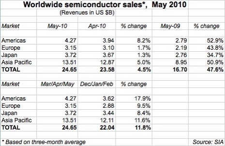
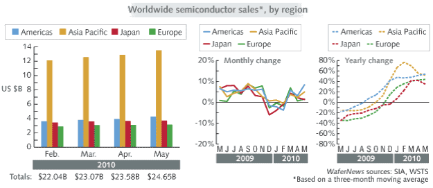
Worldwide chip sales (a three-month moving average) bounced up 4.5% in May — about twice as much as April’s 2.2% M/M growth — to $24.7B. Year-on-year comparisons are starting to fall back to earth, slightly, with "only" ~50% growth vs. May 2009, as year-ago periods start to fall further away from the slump’s nadir of late 2008/early 2009.

That monthly pace keeps overall chip sales on track for the SIA’s projection of ~28% growth for all of 2010, thanks to broad-based strength in sectors ranging from PCs to cell phones, a resurgence of corporate and industrial IT spending, and even automotive, noted SIA president George Scalise, in a statement. PC sales, for example, are expected to spike 20% this year; cell phone unit sales should be up 10%-12%.

Click to Enlarge

Credit Suisse’s John Pitzer dug deeper, noting that the factor in May was strong ASPs (8.1% month/month, vs. seasonal 1.4%) overriding weaker units (-5% vs. seasonal 1.7%). Europe macroeconomic weakness didn’t seem to have an impact, as Europe chip sales rose about in line with seasonal norms (1.6% vs. 1.5%). Taking Y/Y comparisons, the highest increases for device types were DRAM (155% Y/Y) and MCU (63%), with DSPs and logic (24%-25%) on the tail end of growth for the month. By applications, autos (87%) and industrial (62%) led the pack; communications/wireless was basically flat (1%).

If June numbers (ICs excluding memory) are to follow normal seasonal patterns, Pitzer looks for about 5.5% growth (vs. 4.2% guidance and 2.5% normal seasonal growth). And if the rest of the year falls into line with seasonal trends, look for chip sales to rise 25% — but that’s below current outlooks of 28% (and some say maybe 30%+). IC unit shipments (minus memory) remain 6% below long-term trends, he points out.

But despite the ongoing rosy picture, the SIA is still cautioning against ebullience. "Growing concerns about issues such as government debt, declining consumer confidence, and pressures on government spending do not appear to have affected worldwide semiconductor sales to date, but given the semiconductor industry’s growing sensitivity to macroeconomic conditions, these issues bear watching in the second half of 2010," Scalise said.

Click to Enlarge