Category Archives: Uncategorized

April 9, 2010 – New insights into memristors could offer an offramp to the increasingly challenging navigations of Moore’s Law scaling, and some very interesting applications in biomed research.

A memristor ("memory resistor") is the fourth fundamental circuit element (along with resistors, capacitors, and inductors), which together could form a complete set of functions in a wide variety of electronics circuits. Incorporating memristors could eliminate the need for much of the transistors & capacitors, in some cases by an order-of-magnitude, according to Stan Williams, director of HP’s Information & Quantum Systems Lab and lead researcher on the project. And using fewer transistors to achieve the same functionality sidesteps the problem of maintaining Moore’s Law by scaling devices to physics-altering sizes. Memristors also are seen as a potential replacement for memory chips — they are nonvolatile, consume less energy, store twice as much data in the same space, and are highly radiation-resistant.

Two years ago, HP claimed proof of existence of memristors, though some argue that it’s been a popular field of study for years. And speaking last Nov. at a Silicon Valley Engineering Council event, Williams had teased about upcoming new achievements in memristors.

And now, in a paper published in Nature, HP researchers say that they have improved their initial memristor devices so that they are closer in performance to today’s silicon transistors yet at a fraction of the size — and they indeed can perform logic functions, and thus could be used in future microprocessors, made with conventional materials and processes. More immediate use would be in memory chips; HP Labs claims to have a "development-ready architectures" that stack multiple layers of memristor memory on top of each other in a single chip.

Click to Enlarge
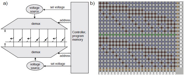
Figure 1. A possible and highly simplified implication logic circuit architecture based on a linear array of memristive switches. (a) A schematic illustration of the architecture with two demultiplexers and two voltage sources, one to deliver the voltage VCOND to the source memristive switch and the other to deliver the voltage VSET to the target switch. Note that with this architecture, the demultiplexers can arbitrarily address any switch to set or clear it and any two switches in the array to implement an IMP operation. (b) A diagram of the linear array of memristive switches shown as green, and the connection pattern of permanently fused (brown) and open (blue) junctions in a crossbar that act as the VCOND and VSET demultiplexers for the switches. Note that the width of the demultiplexers scales as the base two logarithm (log2[N]) of the number of memristive switches in the linear array N, and that in principle there may be many rows of memristive switches M all connected by the same demultiplexers. By loading different initial values into each of the M rows of switches, the same computational sequence can be carried out in parallel to yield M different results. (Source: Nature)

From the Nature paper abstract:

Recently, ultra-dense resistive memory arrays built from various two-terminal semiconductor or insulator thin film devices have been demonstrated. Among these, bipolar voltage-actuated switches have been identified as physical realizations of ‘memristors’ or memristive devices, combining the electrical properties of a memory element and a resistor. Such devices were first hypothesized by Chua in 1971, and are characterized by one or more state variables that define the resistance of the switch depending upon its voltage history.

Here we show that this family of nonlinear dynamical memory devices can also be used for logic operations: we demonstrate that they can execute material implication (IMP), which is a fundamental Boolean logic operation on two variables p and q such that pIMPq is equivalent to (NOTp)ORq. Incorporated within an appropriate circuit, memristive switches can thus perform ‘stateful’ logic operations for which the same devices serve simultaneously as gates (logic) and latches (memory) that use resistance instead of voltage or charge as the physical state variable.

"Memristive devices could change the standard paradigm of computing by enabling calculations to be performed in the chips where data is stored rather than in a specialized central processing unit," stated Williams. "We anticipate the ability to make more compact and power-efficient computing systems well into the future, even after it is no longer possible to make transistors smaller via the traditional Moore’s Law approach.

Moreover, there’s a clear path to some interesting applications for memristors — whose functionality is basically the same as how a brain works. "The flood gate is now open for commercialization of computers that would compute like human brains, which is totally different from the von Neumann architecture underpinning all digital computers," added UC/Berkeley’s Leon Chua, who was involved in the pioneering work in memristors in the 1970s.

Click to Enlarge
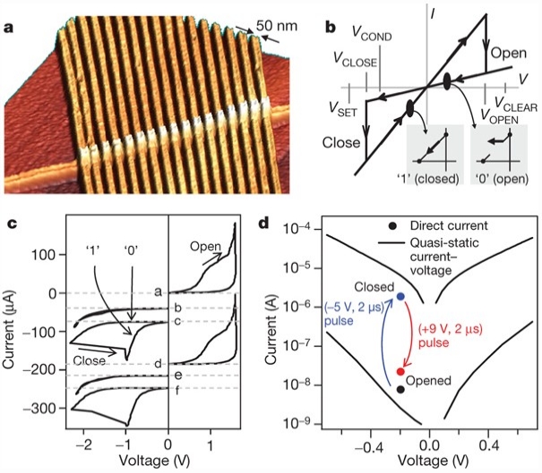
Figure 2. (a) Atomic force microscope micrograph of a nanocircuit. (b) Idealized memristive electrical characteristics, with abrupt voltage thresholds for opening and closing the switch between the low-resistance switch-closed state (logical value ‘1’) and the high-resistance switch-open state (logical value ‘0’). (c) Experimental direct-current current-voltage switching characteristics (four-probe method). Traces b-f are offset. Trace a shows a closed-to-open transition, trace b shows stability and trace c shows an open-to-closed transition. Traces d-f repeat this cycle. (d) Switch toggling by pulsed voltages (2μs long; VSET = -5V and VCLEAR = +9V). Non-destructive reads at -0.2V test the switch state. (Source: Nature)


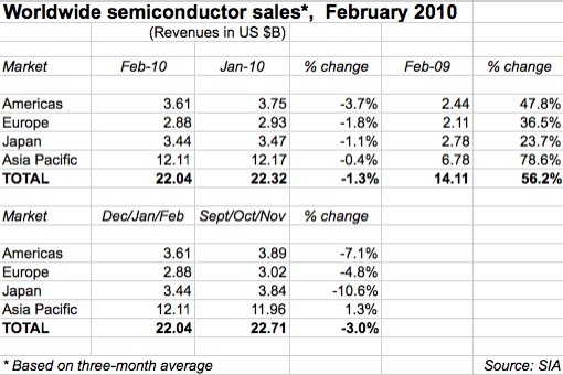
April 5, 2010 – Chip sales slipped a bit in February after a better-than-expected January performance, but overall the market still shows recovering demand particularly in key markets and in emerging economies, according to the latest monthly data from the Semiconductor Industry Association (SIA).

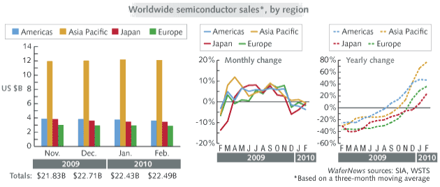
Chip sales (a moving three-month average) decreased -1.3% from January to $22.04B, compared with just $14.11B a year ago (a 56% jump), the bottom of the downturn. By region, all regions lost ground except Japan, which cut its rate of decline in half vs. January (from -2.6% to -1.1%).

Click to Enlarge

Despite the declines, the numbers "reflect continued recovery of sales of semiconductors, with demand principally driven by growth in sales of electronic products in emerging economies," according to SIA president George Scalise, in a statement. Growth "in the low- to mid-teens" is projected this year for PCs and cell phones, he noted; signs indicate the global economic recovery should continue; and there continues to be "upside potential" to beat the group’s initial 2010 forecast in November of $242.1B and ~10% growth.

Click to Enlarge

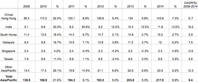
Note that in the SIA’s new numbers, final January chip sales for the broad Asia-Pacific region came in lower than originally tallied: ~$5M lower for Japan ($3.47B vs. $3.52B) and about $110M lower ($12.17B vs. $12.28B) for the rest of the "Asia Pacific" region. Nonetheless this remains by far the largest chip market and a key growth area. Gartner pegs A/P chip sales at nearly $170B in 2010, up >21% from the prior year, and another 9% growth in 2011, thanks again to consumption of PCs and cell phones. Emerging markets in particular offer opportunities — e.g. India and "other" nations (e.g. Vietnam) are seen with higher CAGRs from 2009-2014 than the overall A/P’s 9.4%, thanks to new and upgraded production facilities, government policies, and growing domestic demand. Look for the A/P market to top the milestone $200B level in 2013.

Click to Enlarge
Asia/Pacific country-level semiconductor forecast, 2009-2014, in US $B. (Source: Gartner)


March 24, 2010 – The SOI Industry Consortium and several partners are launching a new "Ready for SOI Technology" program to broaden access to and encourage adoption of silicon-on-insulator technology, which can provide substantial improvements in chip performance and power requirements vs. bulk Si.

The program’s goal is to make available design building blocks to chip designers for new applications such as mobile and consumer products. "The vision for the program is to make the ecosystem visible to designers — to reach out and get the same level of support as they get with bulk IP," explained Jeff Wolf, director of membership development for the SOI consortium and project lead for the "Ready for SOI" program. More specifically, the project addresses one of the key messages gleaned from users: What would it take to adopt SOI? "One was lack of IP for SOI," he said. Formation of this IP program directly addresses this issue "and takes it off the table."

To that end, a "microsite" is now hosted on ChipEstimate.com to help chip designers gain access to those design blocks; the available IP in this program focuses on physical IP, which is typically more difficult to port to SOI than synthesizable IP using industry-standard tools, Wolf pointed out. (A training event, SOI Jump Start Training, will be hosted by Cadence on April 28 in San Jose, CA, both live and as a recorded Webcast.) Key technology partners include IBM, ARM, Boeing (some of which targets a Honeywell process), Cadence, and Synopsys. A quick scan of the SOI portal shows 46 different IP that are available to port to SOI.

Initially the SOI IP focuses on IBM’s 45nm foundry process, since 45nm is mainstream for current foundry sales, Wolf noted. Both the goal is to expand both backward (65nm and 90nm) and forward (32nm), emphasized Wolf and Mendez. Last fall IBM prototyped a 32nm SOI chip and ARM, in fact, is working on SOI at the 22nm node, they pointed out. (Last fall ARM demo’d a test chip based on its 1176 processor using IBM’s 45nm SOI process, with no prior SOI knowledge and using the same resources/timeline as a bulk design — more info on those 1176-on-SOI results are here).

Notable among the IP is IBM’s eDRAM, tipped in late 2009, which offers potential for density and performance improvements. Horatio Mendez, executive director of the SOI Industry Consortium, noted that inclusion of IBM’s eDRAM is key to enabling designs for applications such as data streaming (with stiff requirements for bandwidth capabilities and memory) and consumer applications like digital TV. These are "real-life applications — content that people can be using right away," he said.

Going forward, Mendez and Wolf say they want the program to expand the SOI ecosystem in two key directions: more IP providers, and more foundry support. GlobalFoundries and Freescale (both members of the IBM semiconductor technology alliance) build on SOI, and others have built prototypes on SOI; "virtually everyone has tried to work with it, but it’s a business decision on how to market it," Wolf noted. He added that standard-space IP (e.g. bus interfaces) would probably emerge over time for SOI, following the trend of how general IP has been developed.

by Scotten W. Jones, IC Knowledge LLC

Editor’s note: This letter is in response to "The economic realities of 450mm" by SEMI’s John Ellis.

February 19, 2010 – The possible transition to 450mm wafers would be an enormous undertaking for the entire semiconductor industry ecosystem. Developing the best possible understanding of the trade-offs is critical to good decision-making. A free and open debate about the economics of the transition benefits everyone. I enjoyed reading John Ellis’ article and also following the included links to read some of the material on which it is based. However, I would like to respond to some of the statements made therein, as well as point out some mischaracterizations of my work.Click to Enlarge

Mr. Ellis points out that I have assumed that 450mm tools will have throughput identical to 300mm tools. He goes on to state that "beam tools" will not be able to meet this assumption based on "physics," and cites SEMI’s Equipment Productivity Work Group’s (EPWG) paper on the economics of 450mm for the basis of his statement. I had not previously seen this paper, although I have now read it. Unfortunately the EPWG report only states the throughput without providing any detail that would allow outside parties to evaluate the validity of the conclusion. I do agree that throughput is a critical assumption in my analysis — and later in this letter I will present some calculations using the lower throughputs cited by the EPWG report to show the impact that lower beam tool throughputs would have on cost.

Mr. Ellis states that "IC Knowledge’s assumptions on consumables cost and wafer costs are also not supported by analysis," and "all of the optimistic predictions of cost savings accrued by going to 450mm wafers assume that 450mm wafers will cost approximately the same per unit area as do 300mm wafers." Both of these statements are wrong and do not correctly characterize the analysis that was done for the "300mm Prime and the prospect for 450mm wafers" article. Historically each new wafer size has a much higher cost per unit area for the starting wafer and then over time the cost per unit area comes down until it is close to or equal to the more mature wafer sizes. I have assumed that the starting wafer cost per unit area for 450mm wafers is approximately 5× the cost per unit area of 300mm wafers in 2015, and that assumption is reflected in my analysis presented in the paper. Furthermore, I have assumed that water, energy, gases, chemicals, and other consumables also show increased usage with the larger wafer size and those assumptions are also reflected in my calculations.

Mr. Ellis goes on to say that "IC Knowledge has stated that 300mm Prime will not meet its productivity improvement objectives," this also is not an accurate characterization of my article. What I say in my article in two places is that to-date 300mm prime has not met its productivity goals. I also point out that no one has been able to outline a path to do so, and that this leaves 450mm "on the table."

I would also like to point out that in the writings I have done about 450mm, that while I have concluded that it will produce a wafer cost saving for semiconductor manufacturers, I have also pointed out that the economics for the equipment companies do not look favorable.

The work I have done on 450mm is based on simulating costs using my commercially available IC Knowledge — IC Cost Model. One of the strengths of the model is the ability to easily simulate different assumptions. I have a version of the model modified for 450mm calculations where for each type of equipment – cost, throughput, and footprint multipliers versus 300mm may be set as well as energy, water, chemicals, gases, and other consumables usage. The current ISMI guidelines for 450mm call for no increase in consumables per 450mm wafer vs. 300mm wafers, and also for tool footprints to be the same for the same throughput (taller is OK within reason, or larger is OK if throughput is correspondingly higher). To the best of my knowledge, ISMI has not set tool cost targets. I have used the 450mm version of the cost model to simulate three sets of conditions for a 22nm process produced in 2015. The first is 300mm; the second is 450mm with 1.0× 300mm tool throughputs, footprints and consumable usage; and the third is 450mm with the beam tool throughputs and footprints adjusted based on the EPWG numbers (the footprints are adjusted down in proportion to the throughput reduction). For 450mm I have assumed an average 1.3× increase in tool cost with exposure and some other tools >1.3× and other tools <1.3×. The resulting improvements in wafer cost per unit area are 29% for the 1.0× assumption and 14% for the EPWG assumptions. Please note that in both cases these are 2015 costs that include an approximately 5× cost per unit area increase in starting wafer costs. Over time the starting wafer multiplier should come down further, increasing the cost savings to as much as 37% in the first case and 22% in the second case. As additional projections around tool performance, material cost and other wafer fabrication parameters are developed the 450mm cost modeling tool provides a powerful technique for evaluating the impact on wafer cost.

Conclusion

The 450mm transition continues to be a hotly debated topic. Based on my work to date, I continue to believe that 450mm will produce a wafer cost reduction for semiconductor manufacturers. If 450mm tool throughputs of 1.0× are achieved, then a larger cost reduction results; if lower throughputs are achieved then the cost reduction is smaller. Clearly, companies such as Intel and Samsung agree with this conclusion, or they wouldn’t be pushing so hard for it. From an equipment company perspective, I believe 450mm is problematic with return on investment uncertain at best consistent with the reluctance of most equipment companies to support 450mm.

Biography

Scotten W. Jones received his Bachelors of Science from the U. of Rhode Island, and is a senior member of the IEEE, a member of the Electrochemical Society, and is president of IC Knowledge LLC, P.O. Box 20, Georgetown, MA 01833 USA; 978-352-7610; [email protected], www.icknowledge.com.

by John Ellis, SEMI

February 12, 2010 – For the lifetime of the semiconductor industry, reduced cost and increased functionality have driven end applications and sales. The main lever in achieving both of these has been through the ever-advancing reduction in feature size achieved through the inventiveness and hard work of the engineers and scientists in the industry, government, and universities. Increased functionality through enhanced chip and system design and ingenious software add to the remarkable improvement in electronic systems capability. All of this growth has been built on the performance of the chips themselves. It is no surprise that manufacturers continue to strive for the next improvement, as it is the lifeblood of the entire supply chain.

The changing nature of the industry has presented manufacturers with new realities. The semiconductor industry went through an extended time of incredible growth up until the dot-com bubble. However, growth has slowed considerably as the industry has matured and saturated numerous market segments. The slow growth has led to a significant reduction in the number of fabs required to meet market demand and a smaller market for the suppliers of capital equipment, which ultimately limits the overall amount of R&D resources the supplier community has available for continued improvements.

A SEMI white paper ("Semiconductor Equipment and Materials: Funding the Future") published in October 2005 outlined this looming problem, predicting that by 2010 the industry would need $10.4B to fund basic technology R&D. The industry bust of 2008-2009 has made the situation worse — only $2.1B of the $10.4B needed for R&D will be available as we look forward to 2010. With these constraints the industry has to make hard choices about what will and won’t be funded. Unfortunately, the industry doesn’t operate as one entity, as there are many forces, interests, and objectives at hand, and not all can be satisfied. So, companies have to make very smart choices in their investment choices.

New markets have opened up for many semiconductor suppliers, including photovoltaics, the "Smart Grid", high-brightness LEDs, NEMS/MEMS, and flexible and printed electronics and displays. While all are related to semiconductors, each market requires its own investment in market research, needs assessments, and focused R&D that can further complicate a company’s strategy.

SEMI’s role is to look objectively at the overall market conditions, economic factors, and timing to provide our members with data to make optimal strategic and investment decisions for their own companies. In this vein, we would like to present our perception of the current status of the economics and timing of a 450mm wafer transition.

Economics

There continues to be a pervasive misconception that a wafer-size transition alone can provide a significant cost saving for the industry. Expectations of 30% cost savings have been repeated so often that it may seem that it is a fundamental law of wafer-size transitions. As was pointed out in SEMI’s Equipment Productivity Work Group’s (EPWG) paper on the Economics of 450mm, this expectation has not been based on objective analysis. The following data, based on analysis from our member companies, raise large questions which have been overlooked by IC Knowledge in their assessment. For example, Scotten Jones states that at IC Knowledge:

"We have assumed 450mm equipment will have similar throughput to 300mm and cost 1.3× as much."

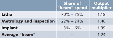
This assumption has not been substantiated by objective analysis. The reality is that beam tools — tools whose throughput is a function of the area they can scan in an hour — can only have their speed increased within certain limitations due to basic physics. (The details of our analysis are available in our EPWG report.) The key is that IC Knowledge assumes the same number of wafers per hour processed, providing the increased area per hour improvement in speed. Beam tools can handle fewer wafers per hour for an equivalent equipment wafer scale up. Whereas IC Knowledge’s multiplier on throughput would be 2.31× (2.25× increased area plus additional gains at the edge), a beam tool’s output multiplier is an average of 1.24×, or almost 50% less (Figure 1). This analysis has been acknowledged by industry groups working with SEMI. IC Knowledge’s assumptions on consumables cost and wafer costs are also not supported by analysis.
Click to Enlarge

All of the optimistic predictions of cost savings accrued by going to 450mm wafers assume that 450mm wafers will cost approximately the same per unit area as do 300mm wafers. However, there are many technical challenges that must be faced by wafer manufacturers to develop the extremely high quality substrates that will be required that will make this assumption hard to achieve. SUMCO offers a detailed analysis of their investigation. Readers are encouraged to download the EPWG analysis which provides details on our analysis.

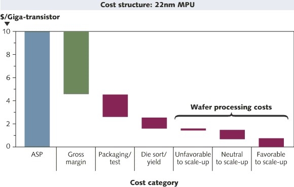
It is important to recognize the overall impact on the industry that a transition to 450mm might have, over and above any potential cost savings in wafer processing. Figure 2 below shows a chart that details the expected cost structure for a 22nm microprocessor. The data are based on IC Knowledge reports. Note that the wafer processing costs make up about 15% of the overall price (to the customer or ASP) of the final product. Even if a reduction of 30% in overall costs were obtained, this would result in a net savings of 5% of the overall part cost, and consumers might see half of this. Our study shows that perhaps 8% of the overall costs would be reduced by a scale-up. This leads to the obvious question — is a projected $25B investment in equipment R&D justified for 8% improvement?
Click to Enlarge

IC Knowledge has stated that 300mm Prime will not meet its productivity improvement objectives. It is a substantial jump to say that 450mm, therefore, is necessary. To conclude that 300mm Prime effort has failed would be misleading. It is our view that the distraction caused by focus on 450mm, along with the massive downturn experienced in 2008-2009, has diluted any serious, concerted efforts toward re-architecting 300mm fabs. We prefer to say that 300mm Prime, or its successor, 300mm Next Generation Factory, has not yet been given a chance.

Timing

Originally, the industry had targeted the transition to 450mm for the 32nm node, but this has now slipped to the 22nm node for production. At the Industry Strategy Symposium held by SEMI in January, 2010, some analysts, e.g. Bob Johnson from Gartner, were predicting that the transition would most likely be 11nm, if it happens at all. This is more consistent with the announcement of 22nm processors occurring in 2011 by Paul Otellini, CEO of Intel. It is also consistent with supplier statements that they cannot afford to develop process technology on two platforms at the same time — the cost is prohibitive and the overall market not big enough to justify the investment. However, ISMI has announced its continued plans for a demonstration program at 32nm and pilot lines at 22nm.

11nm on 450mm wafers?

There are potential benefits in setting 11nm as a target for 450mm introduction. This delay may provide time to wring out the serious technology issues equipment manufacturers must resolve in the non trivial scale-up to 450mm. Recent presentations at the 450mm Workshop at SEMICON Europe 2009, organized by Fraunhofer Institute, show that for most tools there are unforeseen technical impacts that have to be analyzed and dealt with. Funding for research on these difficult areas is strongly encouraged, and SEMI applauds the European Commission for providing a program to help suppliers in these efforts.

However, there are a lot of technology challenges to be overcome at 16nm unrelated to the transition to 450mm. These include: double patterning, EUV lithography, new materials, and complex levels of process integration beyond the capabilities of most equipment suppliers. Knowing that our big lever is feature size reduction, and that there may not be enough R&D funding to do everything, the question is what would we give up, as an industry, if we had to?

What happens at 11nm? There have been implications that new materials, perhaps even a new substrate, will be required. In an extreme case, but unlikely case, we might see that 450mm is a one-node solution.

Funding

Now to the hard part that not even SEMI has fully analyzed. Several analysts have estimated the R&D investment required for suppliers at $25B to $30B (VLSI Research and IC Knowledge). SEMI’s investigations support this number. However, no one has looked at how this effort will be funded. In the 300mm transition, it is generally agreed that suppliers funded the bulk of the R&D required for equipment. It is a more controversial issue to determine whether the suppliers have ever recouped their costs. Forgoing this discussion, we’ll jump into a simple, high-level analysis on whether the supplier community is equipped to fund the R&D needed for 450mm.

In our R&D Funding the Future white paper, SEMI found that suppliers have been able to spend about 14 to 15% of their overall revenue on R&D activities. Recent analysis by SEMI continues to substantiate this amount. Of this total, about 10% is spent on research. The balance of the funding goes toward many activities, including equipment support and continuous improvement. Of course, this funding goes toward all R&D — including technology, e-manufacturing, new business (PV), etc. SEMI’s current estimate for revenue for the equipment industry for 2009 is approximately $14.1B, growing by over 47% in 2010 to $20.74B. If the full 15% of the supplier R&D budget for 2010 was applied toward 450mm, there would be $3.11B available for a 22nm node transition, with slightly more available for a 16nm node transition. Most of this funding is already committed toward funding technology advancements, including process technology, 3D TSV technology, and materials. This amount falls far short of the estimated $25B required for 450mm.

Even if there were substantial cost-savings by moving toward 450mm wafers, the timing and funding issues are serious concerns. A transition to 450mm will be a very difficult undertaking and will require a coordinated effort across the entire supply chain. Only three chipmakers (those with serious capital equipment budgets) have announced support for 450mm, so a coordinated effort seems difficult at this point. Industry Readiness

It is not SEMI’s role to encourage or discourage a particular industry decision. That is ultimately left up to the market. In fact, the SEMI Standards program is actively pursuing development of standards that are 450mm wafer-size specific. If the industry is going to be ready for a transition at some point in the future, these standards are absolutely necessary in order to reduce overall development costs.

Since the supplier industry clearly does not have sufficient funding to tackle the issues surrounding 450mm and keep other technologies on-track, we are supportive of government funding to look into key research issues. We are particularly supportive of funding that can be channeled toward ‘dual-use’ technology improvements that may benefit 300mm now while being applicable toward 450mm later.

A true collaboration from industry, where key stakeholders have contributed substantial funding toward supplier R&D efforts, would be a key sign that the proponents of 450mm are very serious about moving it forward with some "skin in the game". We have not seen this in any significant way.

In the meantime, SEMI will continue to work with industry in evaluating the economic, technology, timing, and funding issues so that our members have as a large set of data upon which to base individual company strategic decisions.

Biography

John Ellis is VP of standards and technology at SEMI.
February 2, 2010 – Continuing with our running theme of industry outlooks for 2010 and beyond, here are three viewpoints recently expressed: Bill McClean from IC Insights with strong optimism macroeconomically all the way down to semiconductors; Terry Brewer from Brewer Science outlining the opportunities for materials suppliers; and Craig Ramsey from CyberOptics Semiconductor, relating how his company withstood a tough 2009 and what it’s doing to ensure 2010 growth.

For a view of 2010 rebound, look in the mirror says IC Insights

Speaking at IC Insights’ 2010 forecast seminar, president Bill McClean told the audience that 2010 will be a mirror image of 2009. However, the equipment suppliers are being squeezed — the capex cycles are so large with a 41% decline in capex in 2009, and now a 45% increase in capex expected in 2010, peak to trough, in two years (see figure), "the equipment guys are at the tail-end of the whip," observed McClean.

Projecting a 60% probability of occurrence, IC Insights sees the IC industry growth rate at between 10%-20%, with several assumptions: worldwide GDP growth between 3.2%-3.8%, a 90%-92% capacity utilization, a 12%-18% growth in IC unit volume shipments, a 6%-8% increase in worldwide electronic system sales, and a change in IC ASP ranging from -2% to +2%.

Click to Enlarge

The industry rebound is unfolding amid stimulus plans being implemented worldwide. McClean pointed out that the bulk of worldwide stimulus packages — which total a little more than $2T — will actually be used in 2010 (55%) with 35% having been used in 2009 and 10% expected to be left over for use in 2011. "The stimulus isn’t running out — we’re just getting started," said McClean.

Specific changes to the supply base noted by McClean include the fab-lite movement gaining momentum, record low capex as a % of sales budgets, and delays in moving production to 450mm. The end result of these trends will be conservative foundry spending leading to a better pricing for the foundries, increased pricing power for IC manufacturers, and overall, long-term stable-to-increasing IC ASPs and IC market CAGRs of 8%-10%. — Debra Vogler, senior technical editor, Solid State Technology

A decade of new materials enabled by robust IP

by Terry Brewer, president/CEO, Brewer Science Inc., Rolla, MO USA

The large wheel of change, as opposed to the smaller wheels of shorter cycles, is turning. This change bodes well for materials in general, and energy-enabling materials in particular. The decade of new materials is upon us, and it will be the driver for the next generation of semiconductor products. The last 30 years have seen exponential increases in the complexity and use of materials in the electronics industry. Innovative hardmask and double pattern materials using immersion lithography, and other materials such as EUV and electron beam will begin the wave of the future to meet specifications in the logic and memory segments below 32nm.

The economic downturn this past year provided an opportunity for materials suppliers to deliver innovative solutions that benefit multiple markets in terms of cost reduction and greater efficiencies. For example, organic materials in support of the solar cell industry, as well as materials to enable advanced packaging, such as temporary and permanent bonding, offer material suppliers innumerable opportunities to develop unique market spaces. Dedicated investment in research and development must be continuous in order for the industry to design these new market spaces.

The US government will again become a major partner and customer in the creation of new products and market spaces. While we are still in a period of economic transition, governments across the globe will play a critical role in positioning nations for long-term growth and competitiveness. In the next decade, US leaders should foster an innovation economy to enable domestic companies to be globally competitive and allow them to protect valuable intellectual property.

A key element that contributes to a country’s global competitiveness is the robustness of its IP. The US must step up to strengthen and safeguard IP rights in the global economy — the domestic economy is driven by innovation and creativity, and nearly one-half of all exports are from IP-based industries. With more than $5 trillion of its GDP based upon IP, the US should be setting the gold standard for IP rights and protection. Much more can be done in the next few years to regain a competitive edge in this country and to send a clear message that the US will persist in its efforts to ensure the integrity of US IP.

Buckling down in the downturn — now buckle up for the rebound

by Craig C. Ramsey, general manager, CyberOptics Semiconductor Inc., Wilsonville, OR USA

The global recession was tough overall and particularly challenging for suppliers to this industry, including CyberOptics Semiconductor. As in previous down cycles, we maintained our technology development initiatives and increased the efficiency of our production systems. During 2009, we expanded our WaferSense product line by developing a sensor for airborne particles and software that reduces the end-user skills needed to solve vibration-related yield loss and downtime. We also consolidated our final assembly and test activities into our parent company’s ISO-9001 registered facility. Finally, we sampled 450mm wafer-like sensors to support the industry’s push for enhanced productivity in the next-generation fab through ISMI’s 450mm program.

Semiconductor technology improves the efficiency and quality of human life. Advancements in device capability and power efficiency coupled with ongoing reductions in economic and environmental cost underpin long-term increases in global prosperity. In 2010, the economy and our industry will be boosted by a variety of forces: continued innovation and growth among smartphone and netbook manufacturers; adoption of Windows 7; growth in the display market; investment in alternative energy; and adoption of hybrid vehicles. Our industry will leverage the recovering demand and embrace technologies that raise production and yield during a time of margin pressure, shrinking tolerances, and reduced infrastructure. Happy New Year, indeed!

February 1, 2010 – Healthy end-market demand in consumer electronics, and now signs of recovery in the corporate IT sector as well, bode well for chip sales as finally show emergence from the downturn and return to normal seasonal patters, according to the Semiconductor Industry Association (SIA).

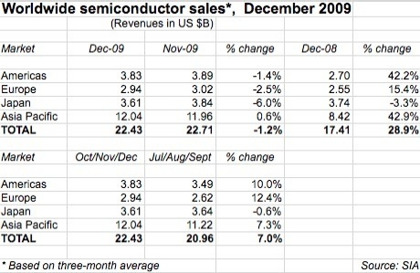
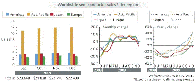
The group’s latest monthly figures show significant improvement in year-ago comparisons: Overall December sales were nearly 30% higher than Dec.2008, with >42% growth in both the Americas and Asia-Pacific. Japan improved slightly but still showed a decline from a year ago, indicating its struggles not only in the chip industry but also macroeconomically as well.

Compared with November, overall chip sales actually dipped a bit: -1.2% overall, with only Asia-Pacific managing to squeak out growth (though as the largest region by far that’s a good sign). And the three-month moving average, while slower than in recent periods, still indicates good growth across nearly all regions.

Click to Enlarge

In the end, 2009 finished with $226.3B in sales, just a -9% decline from the prior year — better than most had thought earlier in the year (and even better than updated forecasts in late fall), attributed from several camps to smart management of inventories.

"In 2010, unit sales of personal computers and cell phones — which account for approximately 60 percent of total semiconductor consumption — will grow in the low-to-mid teens, providing a solid platform for chip sales," stated SIA president George Scalise, in a statement. "We are also seeing the effects of recovery in the enterprise sector and we believe this trend will continue," he added.

In addition, China and India are coming forth as demand-driving emerging markets, Scalise added — both are purchasing PCs and handsets, but also investing in wired/wireless infrastructures, which in turn create more demand for products and applications requiring more semiconductor consumption.

The SIA projects an official return to seasonality with a "modest slowdown" in 1Q10. "With improving consumer confidence and signs of economic recovery around the world, the semiconductor industry is well positioned for growth in 2010," he said.

Click to Enlarge

January 29, 2010 – A second window of opportunity to sell a controlling stake in Korea’s Hynix Semiconductor has come and gone with no bidders coming forward, so the company’s investors are looking at other ways to slough off their interest, according to multiple reports.

Domestic conglomerate Hyosung Corp. pulled out last November after being groomed as a potential investor to take a ~28% stake worth about $3B. A second window of opportunity was opened Dec. 20 inviting new bids, but closes Jan. 29, apparently with no takers, according to the state-owned Korea Exchange Bank (KEB). (After a rebound in recent months, that 28% stake would be valued at about $3.3B, perhaps seen as too big a pill to swallow by investors, the Wall Street Journal suggests.)

KEB says shareholders will examine other ways to get rid of their stake, including selling off ownership in chunks. "The stake sale seems an uneasy task, because there aren’t many companies out there that can afford to buy such a big company and as Hynix may need massive amounts of money for its technology migration," said Lee Min-hee, an analyst at Dongbu Securities, quoted by the WSJ. "Maybe the best way the creditors could come up with will be selling their stake in a block trade or selling it to some financial investors from both at home and overseas." Creditors would prefer to entertain inquiries from domestic investors so as to preserve the domestic chip industry, though foreign investors could invest through domestic firms, noted Ryu Jae-han, president of Korea Finance Corp. (KoFC), quoted by the Korea Times.

January 25, 2010 – Despite reported warnings of inventory bloat at electronic distributors, nearly all segments of the chip supply chain remain lean, according to a report from iSuppli.

On the contrary, instead of a reputed increase in semiconductor inventories in 3Q09, inventory levels at distributors "are well below the historical average," notes iSuppli analyst Carlo Ciriello, in a statement.

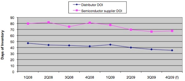
Distributors’ days-of-inventory (DOI) at the end of 3Q09 was actually down 15% from the same time a year ago; in dollar terms that equaled $4.8B worth of chips, which was down 22% from 3Q08. That distributor DOI was 17% less than the trailing three-year average, according to the firm.

Going forward, DOI is expected to have continued to decline in 4Q09 (to 18.7% below the three-year average), vs. a slight incline in inventory dollars. The decline in stockpiles parallels that among chipmakers, who saw their DOI shrink to 66.4 in 3Q09, down 11% from the same period a year ago.

  1Q08 2Q08 3Q08 4Q08 1Q09 2Q09 3Q09 4Q09 (f)
Distributor DOI 47.2 44.1 43.4 42.1 44.7 39.9 36.9 35.3
Semiconductor supplier DOI 79.8 81.9 74.6 81.2 77.4 69.6 66.4 67.5

"Semiconductor suppliers have been maintaining tight control over inventories," preferring just-in-time fulfillment instead of "capital-constraining shelf stocking," according to Ciriello. "This has resulted in lower inventories throughout the electronics supply chain, including at distributors."

Chip inventories are at low levels for most other segments of the electronics supply chain as well, according to iSuppli — makers of PCs, storage devices including hard-disk drives, and cell phones also saw semiconductor DOI in 4Q09 lower than historical levels. Any increase in demand for those end products likely will translate directly into new chip sales. (iSuppli noted comments about inventories during Intel’s recent quarterly results conference call, citing "much stronger sell-through and lower year-over-year inventory levels," as well as an internal "healthy level of inventory" relative to demand.)

The recovery of the chip industry in 2H09 can be directly attributed to just this "deft management of semiconductor inventories," iSuppli notes. And as demand recovers, these lean inventory levels will continue to drive the market’s return to growth in 2010: 15.4% growth in revenues, vs. a -12.4% decline in 2009, the firm predicts.

Click to Enlarge
Quarterly DOI among distributors and semiconductor suppliers, 2008-2009. (Source: iSuppli)


January 20, 2009 –  Having spun off its chip manufacturing operations into GlobalFoundries, AMD has positioned itself as the No.2 global fabless IC supplier in terms of sales, second only to Qualcomm, according to IC Insights.

The top 25 fabless companies collectively suffered in 2009 like everyone else, with sales declining 13%—but the top 10 did notably better, with just a 4% decline in sales, meaning their share of the overall fabless sector rose to 65%, up five points from 2007. Rising barriers to entry (high design costs, increasingly difficult access to venture capital money, etc.) means that this top grouping will likely increase its lion’s share of the market.

Note that all but one of the top 10 companies, and 17 of the top 25, are based in the US. The presence of just a single Japanese company (MegaChips, No.19) indicates domestic resistance to the fabless/foundry model, IC Insights suggests. Also note that of the five companies managing double-digit growth in 2009, four of them were from Taiwan; the island’s fabless firms in particular "staged a strong comeback" in 2H09, the analyst firm notes. MediaTek, for example, posted a 22% gain in 2009, impressive for its $3.5B size. Expect more Taiwanese (and Chinese) fabless firms to make this list in future years as their IC design houses proliferate.

Top 25 fabless IC suppliers. (Source: IC Insights)