Category Archives: Uncategorized

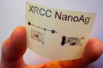
October 30, 2009 – Xerox researchers say they’ve development a new silver ink to print conductors, the third required material necessary for printing plastic circuits to replace silicon.

Click to Enlarge"For years, there’s been a global race to find a low-cost way to manufacture plastic circuits," said Paul Smith, laboratory manager at Xerox Research Centre of Canada, in a statement. "We’ve found the silver bullet that could make things like electronic clothing and inexpensive games a reality today," and enable capability for low-cost printed electronics on a wide scale of materials.

ICs consist of three components: a semiconductor, conductor, and dielectric element. The new Xerox work involves creation of a silver ink to print the conductor like a continuous feed document — using conventional inkjet printing methods — without requiring a typical semiconductor fab cleanroom. Researchers also have improved their existing semiconductor ink to be more reliable, formulated so that molecules precisely align themselves in the most electrically-conductive configuration.

Applications for easily-printed electronics abound: low-cost RFID tags, e-readers and signs, sensors, solar cells, and even textiles/wearable electronics woven into clothing. "We will be able to print circuits in almost any size from smaller custom-sized circuits to larger formats such as wider rolls of plastic sheets — unheard of in today’s silicon-wafer industry," stated Hadi Mahabadi, VP and center manager of Xerox Research Centre Canada.

R&D samples are available by contacting the company.

October 19, 2009 – Now that everyone’s had their spin on Intel’s generally upbeat quarter, let’s boil it down to a few key bullet points:

Growth and profits. Sales, profit margins, and earnings were all well beyond expectations: Sales were $9.4B, vs. Street’s $9.0B; net income $1.9B/EPS $0.33, vs. Street’s $0.28. And gross margins were 57.6% vs. 50.8% in 2Q, attributed in part to savings from reusing 45nm capacity for its new 32nm manufacturing. For 4Q Intel sees sales rising to $10.1B, and gross margins rising to 62%.

"Gross margins stole the show," writes Broadpoint AmTech Research’s Doug Freedman, which "reflect impressive MPU and chipset shipments and minimal mix impact from strong Atom sales." Intel execs and analysts generally agreed that the norm for margins should be somewhat less than 60%, though. Craig Berger with FBR Capital Markets wrote that he is "encouraged" by tangible benefits from "leaner factory headcount, improving production cycle-times, and more equipment reuse between process nodes (including 32nm). Intel probably could ramp revenues to $11.5B if demand calls for it, and net profit could surge to EPS $0.56, he added.

Demand. Corporate spending is still weak, but Intel execs are confident that an upgrade cycle is approaching for the fleet of aging business technology. And the trend of lower-end "netbooks" is still going strong and helping the bottom line, because the chips use trailing-edge technology and have great profit margins. It’s still the core PC market that drives the industry train, though, and Otellini said he "wouldn’t argue" with projections of 10% (or more) PC unit growth in 2010, and that Intel likely wouldn’t exceeded that growth.

Related to the foreseen corporate spending refresh is the timeliness of the anticipated Windows 7. Otellini noted that despite "a lot of excitement about" Windows 7 there seems to have had not much impact on the purchasing climate, but that there is "a lot of interest" around Windows 7 and Intel’s new Nehalem-based SKUs; he sees evals happening through this year and purchases on a refresh basis in 2010.

Inventories. Related to demand is the persistent question whether inventories are being rebuilt in anticipation of, rather than direct response to, rebounding demand — if it’s the former, the industry could find itself with a backlog to work down at the beginning of 2010, which would dent and delay hopes for a chip industry recovery.

Intel execs, though, says things are well-positioned on the stocking front:

[CEO Paul Otellini]: We watched supply chain inventory very carefully and believe the pipeline has been appropriately rebuilt to support increased end demand and yet remains well below the peak we saw at the end of 2008.

 [CFO Stacy Smith]: From an internal inventory standpoint, we’re lower than I like right now. We want to get some inventory in place in Q4. Part of that is we’re just running a little leaner. We were surprised by some of the unit upsides we saw over the course of the third quarter and we want to replenish.

(Smith added later that he wants to "grow inventories modestly" in 4Q09.

Capex. With one quarter remaining in its fiscal year, Intel tweaked its forecast for 2010 capital spending down to $4.5B, about $200M below previous estimates. The company tends to reinvest more intensely in downturns and had generally been expected to lag behind the rest of the industry with capex in the coming quarters, so few really noticed or cared. Cowen’s Raj Seth calls it a "minor negative" overshadowed by the bigger picture of an anticipated 30%-40%+ rebound in overall industry capex.
October 12, 2009 – JSC Sitronics and the Russian Corporation of Nanotechnologies (RUSNANO) have signed an agreement to "launch full-scale production" on a 90nm microchip production line. The investment will be in cooperation with Sitronics divisions Sistema and NIIME and Mikron at facilities in Zelenograd, Russia.

Terms of the deal peg the total investment at nearly $560M, split roughly 60-40 with Sitronics as the lead investor; Sitronics will invest "an equal amount" for tools to be provided by NIIME and Mikron. New facilities incorporating research, design, and production will be built "on the basis of" the existing facilities of the two units. No details about planned production capacities (at startup or full capacity) were provided, though in a statement the groups said end products would target a wide range of end applications, from digital TVs, GPS navigation systems, and smart cards to industrial automation and automotive electronics.

The new 90nm line "is of considerable strategic importance for Russia," and "plays an invaluable role in the development of the Russian high-tech sector and the country’s overall technological security," said Anatoly Chubais, CEO of RUSNANO, in a statement. Gennady Krasnikov, general director of NIIME and Mikron, noted that the company’s migration to 90nm "will enable us to enter new markets while maintaining market leading positions for our 180nm products."

October 12, 2009 – After three years (2005-2007) of solid double-digit growth, third-party chip design service firms saw growth stumble in 2008, fall hard in 2009, and how they address three key challenges will decide the landscape of the sector over the next five years, according to a new report from Gartner.

The economic & industry slumps not only dented the sector’s growth, but also have caused "drastic change" in the landscape for chip design services. In addition to responding to customers’ pressure to add value, such firms must also deal with three key factors, writes Gartner analyst Ganesh Ramamoorthy: shrinking available market for outsourcing, lagging design productivity growth, and fewer/more costly skilled workers.

How they do this will likely revolve around four strategies (either standalone or in some combination), depending on their size and market position and who their customers are:

Align sales and marketing strategy with prevailing design start trends;

Broaden the service portfolio to include product engineering services and other design support services;

Explore mergers and acquisitions to widen service offerings, skill-set capabilities, and geographical reach; and

Understand and analyze regional design start trends, while examining prospects and opportunities.

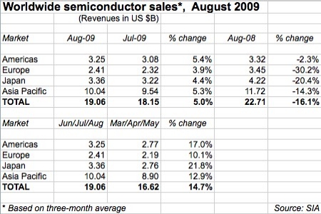
October 5, 2009 – Global semiconductor sales continued to rebound in August, rising 5% from the previous month, according to the latest data from the Semiconductor Industry Association (SIA).
Click to Enlarge
Chip sales in August totaled $19.1B, vs. $18.2B in July. That’s two straight months of ~5% growth to start the third quarter of 2009.

Things are still down from a year ago (-16% in August 2008’s $22.7B), and year-to-date chip sales through August were $133.8B, about -21% below Jan-Aug. 2008 — but we’re nearing the point where things really started to go south a year ago, though, so the Y/Y comparisons should continue to markedly improve.

Of note in the August numbers are slight improvements across all regions. Over the past month (data is a three-month moving average), noticeable pickups were seen in both Europe (5.3% growth, vs. 3.9% M/M growth in July) and Japan (7.9% vs. 4.4%).

Concerns have been floated about chip sales reflecting inventory restocking instead of a true end-demand pull, and a decline in Asia-Pacific chip sales might reflect this. A-P sales growth in August slowed a bit to 4.3% from 5.3% in July; for the moving three-month average, A-P growth dropped slightly from 14.6% to 12.9%. Improvements in other regions, though, kept the total three-month average numbers at nearly 15% growth (June-July-August vs. March-April-May).

Indeed, in an analysis of the SIA numbers, iSuppli says the strong sequential growth in July and August should pave the way for >10% growth in all of 3Q09 — but that’s largely due to an inventory rebuild, and in fact chip sales in 3Q will exceed true demand by about 3%.

Jim Ohlsen, director of materials characterization at Entegris, discusses methods to improve yield at 32nm by controlling molecular contaminants in microenvironments. He also describes the multiple solutions that will be needed at 22nm to keep molecular contaminants at very low levels for long periods of time.

Microenvironments at 22nm


August 4, 2009

Chuck Extrand, principal scientist at Entegris, discusses the impact that constituents such as oxygen and water have on microenvironments at advanced nodes and the challenges that face the industry with respect to purging. He also describes the multi-pronged approach that will be needed to ensure microenvironments meet process requirements at 22nm.

by Xavier Alcaraz, principal consultant, and Andy McIntyre, executive VP/managing principal/cofounder, EORM

July 31, 2009 — Photovoltaic (PV) technologies have experienced significant improvements in efficiency and greater consumer demand, resulting in many more product alternatives and applications than ever before. Newer alternatives to standard crystalline silicon modules have emerged including casting wafers instead of sawing, thin film (CdTe, CIGS, amorphous Si, and microcrystalline Si), concentrator modules, Sliver cells and continuous printing processes. These advances in PV technologies have introduced a range of new manufacturing and R&D chemical and physical hazards that require appropriate engineering, administrative and personal protective equipment controls to minimize the potential for employee illness and/or injuries.

Summary of chemical hazards

PV manufacturing and R&D process present a diverse range of chemical-related health and safety considerations during both production and maintenance operations:

  • Pyrophoric, flammable and/or toxic gases such as silane, phosphine, hydrazine, hydrogen, ammonia, and arsine, which are utilized in reactors to facilitate deposition processes, doping, and for other production-related processes. Worker exposures and chemical safety hazards associated with storage, handling, and transport of these gasses are ever present. Due to the hazardous nature of these chemicals and the potential catastrophic consequences associated with their release or exposure, a detailed process hazard analysis (PHA) should be incorporated into the process design phase. In the US, the type(s) and volume(s) of these chemicals stored at a facility may trigger required compliance with the Occupational Safety and Health Administration’s (OSHA) Process Safety Management standard and/or the Environmental Protection Agency (USEPA) Federal Accidental Release Prevention (FedARP) Program.
  • Mixtures of airborne metal dust, generated from cutting and scribing of solar cells with deposited metals (e.g., arsenic, cadmium, copper, indium, gallium, and selenium), may result in worker inhalation exposure. If cutting and scribing operations are not properly controlled through process enclosure and/or ventilation, airborne emissions of metal dusts have the potential to settle onto equipment, work surfaces and floors creating a potential cross-contamination issue as well as an ingestion hazard to workers. Appropriate assessment of the process and installation of enclosures and/or ventilation controls (if necessary) may be required to adequately control emissions from cutting and scribing, thereby ensuring worker exposures are below the applicable regulatory exposure limits.
  • Nanoparticles used in PV manufacturing such as quantum dots suspended in ink, nanowires, and silver cells are made of various chemicals such as cadmium, silicon, cadmium telluride, and cadmium selenide. Handling nanoparticles in their raw (unbound) form can result in an inhalation and/or dermal hazard. The properties of these nano-sized particles may differ significantly from the larger particles of the same material, including mobility throughout the body, bioaccumulation in select organs, and toxicological response.
  • Various corrosive chemicals used to etch and clean PV components during manufacturing include hydrochloric acid, hydrofluoric acid, phosphoric acid, and sodium hydroxide. Proper ventilation controls, employee training, and use of personal protective equipment (gloves, goggles, faceshields, etc.) are necessary to avoid the potential for inhalation of vapors and/or skin contact.
  • Abrasive cleaning methods are often used to manually clean reactors and other production equipment in CIS and CIGS (copper, indium, gallium, selenium) solar cell production operations, resulting in the potential for exposure to reactor chamber deposits and reactant residues. As such, exposure controls such as “snorkel” exhaust ventilation, use of HEPA-rated vacuums, and cartridge respirators are necessary to minimize worker inhalation exposures.

A broad range of chemical compounds are employed in the photovoltaic manufacturing and R&D processes, some of which have limited toxicological data available and/or no established airborne occupational exposure limits. In the absence of sufficient toxicology data and recommended occupational exposure limits, PV manufacturers should employ a robust combination of engineering controls, administrative practices and personal protective equipment to minimize the potential exposure to workers during production and related maintenance activities.

Summary of physical hazards

In addition to the chemical-related health and safety considerations, PV manufacturing and R&D also present various physical safety considerations during production and maintenance operations:

  • Servicing, cleaning, adjustment, and/or repair of equipment present potential exposure to a range of hazardous energies — electrical, hydraulic, mechanical, etc. Implementation and training on well-written hazardous energy control procedures is critical to avoid the potential for electrocution, amputation, or crushing injuries.
  • Exposed belts, wheels, and other rotating equipment on conveyors or other production equipment require appropriate guarding to prevent inadvertent contact by production and maintenance employees.
  • Use of hand and power tools for machining of parts, preventative maintenance, etc., must be used correctly to avoid injury.
  • Manual material handling of product, equipment, etc. can result in costly sprains, strains, and other musculoskeletal injuries. Use of conveyor systems, crane and hoist devices, pallet jacks, carts/dollies, etc. serve to minimize such injuries.
  • Traffic associated with forklifts, pallet jacks, and other material handling equipment can lead to impact injuries. Operator training and compliance with the Powered Industrial Trucks standards and best practices is required.
  • Cluttered or spilled materials in walkways and general work areas often lead to slip and trip injuries that are otherwise easily preventable.

PV technologies have introduced new manufacturing and R&D processes that present a range of chemical and physical hazards that require careful, upfront planning using a Design for Environmental Safety & Health (DFESH) approach, institution of a robust equipment installation safety signoff process, and proactive management focus on developing and supporting a strong EHS culture to ensure appropriate control of chemical and physical hazards associated with production processes and maintenance interface. Integrating EHS into the business from design to product take-back will contribute to improved employee morale and retention, reduced accident and injury experience, and bottom-line financial contribution.

Xavier Alcaraz is principal consultant at Environmental and Occupational Risk Management (EORM). E-mail: [email protected].

Andrew McIntyre is managing principal and co-founder of Environmental and Occupational Risk Management (EORM). E-mail: [email protected].


This article was originally published by Photovoltaics World.

July 22, 2009 – The global breadth suppliers of photovoltaic cells and panels continued to ploy out in 2008, as several competitors across the globe continue to push past Japan’s major suppliers who once held the lion’s share of the market, according to data from IC Insights.

Sharp, the No. 1 PV device supplier for years, was overtaken in 2007 by both Q-Cells and Suntech Power Holdings. In 2008 it was US-based First Solar who “blew past both Sharp and Suntech” with its cadmium telluride (CdTe)-based thin-film panels — its sales more than doubled (144%) launching it to the No. 2 position, the firm notes in a new report, “Solar Energy: Growth Opportunities for the Semiconductor Industry”.


Top 10 photovoltaic device suppliers in 2008, cell and thin-film panels. (Source: IC Insights, company reports)
CLICK HERE to view larger image

Other notable climbers in the list came from China (JA Solar +109% sales growth, and Yingli Green Energy +93% growth) and Taiwan (Motech 67% growth, Gintech 144% growth). JA Solar and Gintech are solely involved in solar cell production, following the business model of Q-Cells which is diversifying beyond pure-play PV cell manufacturing, the report notes. Other suppliers in the top 10 ranks are involved in everything from panel manufacturing to system installations and other aspects of the solar value chain.

Solar World, No. 10 on the list, is a German company that actually is the biggest PV cell manufacturer in the US, after expanding operations in Hillsboro, OR. And SunPower, a US-based cell manufacturer who makes cells out of the Philippines, barely missed the top 10 list in 2008.

Don’t count Sharp out just yet, though. The IC Insights report, penned by Jeremy Young, notes that Sharp has “extremely ambitious plans” to expand its capacity for silicon-based thin-film panels, and “could quickly make up for lost ground.”

The rankings are based on the peak-MW value of the PV devices produced and sold by each supplier, including PV cells and also panels (for thin-film vendors) — but not cell-based panels, in order to avoid double-counting, the firm notes.

Silicon Genesis president & CEO, Francois Henley, showcases the company’s 20μm kerf-free foil, which is particularly well-suited to BIPV applications and capable of being made into solar cells with 20% efficiency.

He also discusses the company’s progress in bringing the technology to market. Perhaps the main issue will be the ability of manufacturers to handle such ultra-thin foils — but he discusses solutions for that as well.